

Page 1

Hybrid Printer
HSP7000 series
Technical Manual
[ FOURTH
EDITION
]
Page 2

NOTICE
All rights reserved. Reproduction of any part of this manual in any form whatsoever, without STAR’s express
•
permission is forbidden.
e contents of this manual are subject to change without notice.
•
All eorts have been made to ensure the accuracy of the contents of this manual at the time of going to press.
•
However, should any errors be detected, STAR would greatly appreciate being informed of them.
e above notwithstanding, STAR can assume no responsibility for any errors in this manual.
•
© Copyright 2008-2009 Star Micronics Co.,Ltd.
Page 3

INTRODUCTION
is manual describes the thermal printer HSP7000 series.
It is designed for use as a reference for periodic inspections and maintenance procedures to be executed by
service personnel. It is not intended for the general user. Users of this manual should have a basic knowledge
and understanding of the English language.
• is manual is divided into the following sections:
Chapter 1 Adjustments
Chapter 2 Parts Replacement
Chapter 3 Maintenance and Lubrication
Chapter 4 Parts List
• First edition : Aug. 2008
Second edition : Sep. 2008
ird edition : Feb. 2009
Fourth edition : Aug. 2009
Page 4

CHAPTER 1
ADJUSTMENTS
is printer has undergone various adjustments so that it will attain a given standard of performance.
In this chapter, a brief explanation is given of the methods for making adjustments.
Follow the instructions when performing maintenance inspections or when replacing parts to correct malfunctions.
1. Adjusting the Impact Head and Platen Gap . . . . . . . . . . . . . . . . . . . . . . . .2
1-1. Measuring the Impact Head and Platen Gap . . . . . . . . . . . . . . . . . . . . . 2
1-2. Adjusting the Impact Head and Platen . . . . . . . . . . . . . . . . . . . . . . . . . . . 2
2. Adjusting the Printing Dot Mis-positioning . . . . . . . . . . . . . . . . . . . . . . . .3
3. Adjusting the Sensor . . . . . . . . . . . . . . . . . . . . . . . . . . . . . . . . . . . . . . . . . . . . 5
3-1. PE Sensor Adjustment Mode . . . . . . . . . . . . . . . . . . . . . . . . . . . . . . . . . . . . 5
3-2. NE Sensor Adjustment Mode. . . . . . . . . . . . . . . . . . . . . . . . . . . . . . . . . . . . 6
3-3. BOF Sensor Adjustment Mode . . . . . . . . . . . . . . . . . . . . . . . . . . . . . . . . . . 6
3-4. COF Sensor Adjustment Mode . . . . . . . . . . . . . . . . . . . . . . . . . . . . . . . . . . 7
3-5. TOF Sensor Adjustment Mode . . . . . . . . . . . . . . . . . . . . . . . . . . . . . . . . . . 8
Page 5

1. Adjusting the Impact Head and Platen Gap
[4 ][5 ]
[1 ]
[3 ]
[2 ]
1-1. Measuring the Print Head and Platen Gap
1. Insert a thickness gauge [3] between the print head [1] and
platen [2] to measure the gap.
T
o determine the gap, allow the thickness gauge to fall under
its own weight.
Measure the thickness at positions right edge and le edge
2.
of the printing range. (Refer to a gure 1-2)
Note: After closing the platen frame and allowing the
rollers to contact each other, wait 5 minutes or
longer for the expansion and contraction of the
rubber material to settle. Then, measure the gap.
Between the print head and platen
Reference values for the gap : 0.24 to 0.29 mm
3. If the gap is not at the standard value, see page 1-2 to adjust
the gap.
Fig. 1-1 Measuring the Gap
1-2. Adjusting the Print Head and Platen
1. To adjust the le side gap, remove the adjustment bushing
[5] screw [4] in the platen frame L and move the adjustment
bushing [5] up and down.
T
o adjust the right side gap, remove the adjustment bushing
screw in the platen frame R and move the adjustment
bushing up and down.
M
ove it in the "+" direction to increase the gap, and "-"
direction to decrease it.
Note: Be carefu l not to ope n the platen frame whil e
adjusting the platen.
2. Measure the gap as described in 1-1 above.
3. After obtaining the desired amount of gap, tighten the
loosened screws.
Note: The gap tends to increase during the reinstallation
of the upper case. Therefore, be sure to recheck the
gap after reinstalling the upper case.
Printing range
Fig. 1-2 Printing range
Fig. 1-3 Adjusting the Gap (Left)
- 2 -
Page 6

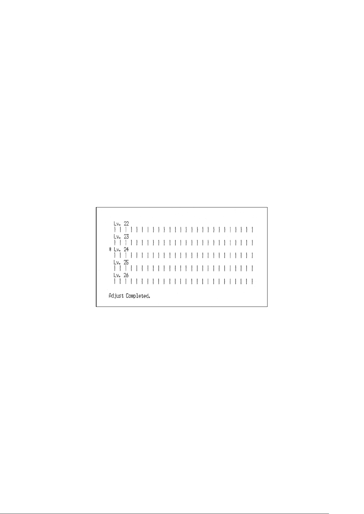
2. Impact Head Printing Dot Alignment Adjustment Mode
往路
復路
往路
(1) With the front cover open, turn the power ON while keeping the RELEASE button pressed.
(2) Close the front cover and place the paper in the printer. en, the printer will print “Dot Alignment Adjust Mode” and
enter the impact head dot alignment adjustment mode. e printer will continue printing a total of 22 patterns of dot
alignment adjustments as shown below. e patterns are staggered in 1/8-dot increments.
e printed line above each pattern shows a number between 1 and 23 and its setting value (Lv.xx). e pattern preceded
by a “*” mark indicates the present setting value.
As shown below, the adjustment patterns that are printed consist of a three-dot bar each at the top and bottom for the
(3)
forward pass, and a three-dot bar in the middle for the backward pass. Check the patterns visually and select a pattern
with the three bars forming the straightest line.
Forward pass
Backward pass
F
orward pass
Improper
correction
(4)
To set up a pattern, press the RELEASE button as many times as the number (1 to 23) of the desired pattern. In the
Optimal
correction
Improper
correction
process, a buzzer will make a short sound (0.1 second) with each pressing of the RELEASE button.
(5)
Repeat step (4). At the pattern number that you wish to accept, keep the RELEASE button depressed (approx. 2 seconds)
until the buzzer makes a long (0.5 second) sound. is completes the acceptance of the setting.
Example: To accept the No. 4 setting, short-press the RELEASE button three times. At the fourth time, keep the
RELEASE button depressed.
Note:
This will cause the warning buzzer (0.1 second) to sound four times, and will delete the number of pressings
If you press the RELEASE button 24 or more times, it will exceed the available range of settings.
of the button. Go back to step (4) to resume the setup process.
- 3 -
Page 7
(6) If you do not find an optimal correction pattern among the printed patterns, perform the “Backward” or “Forward”
operation as indicated in No. 1. ese operations will allow you to make printing pattern adjustments with a greater
range of dot corrections. Aer performing steps (1) to (3), perform the respective operations as follows:
or a “Backward” operation, keep the RELEASE button depressed (approx. 2 seconds) until the buzzer makes a long (0.5
F
second) sound.
e printer will release the paper with a printing pattern in which the backward pass is corrected rightward of the
→
current printing pattern.
or a “Forward” operation, keep the RELEASE button depressed until the buzzer makes a long (0.5 second) sound. en,
F
continue pressing and holding (approx. 4 seconds) the RELEASE button until the buzzer makes a short (0.1 second)
sound and another long (0.5 second) sound.
→
The printer will release the paper with a printing pattern in which the backward pass is corrected leftward of the
current printing pattern.
(7)
The printer will write the setting value, which you have accepted, on the nonvolatile memory. For confirmation, the
printer will print out ve patterns (which includes the setting value that you have accepted, as well as the preceding and
succeeding patterns) and an “Adjust Completed” message. is is followed by the release of the paper and the resetting of
the printer.
Note: During the period between the time you accepted the setting value and the printer starts to print as
described above, the printer will write the setting value on the memory. Never turn the power OFF or reset
the printer during this period. Doing so will corrupt the dot adjustment settings as well as other settings.
If you make a mistake in the settings, do not turn the power OFF in the middle of the process. Instead, wait
until the printer completes the nal reset and start the dot adjustment mode from the beginning.
- 4 -
Page 8
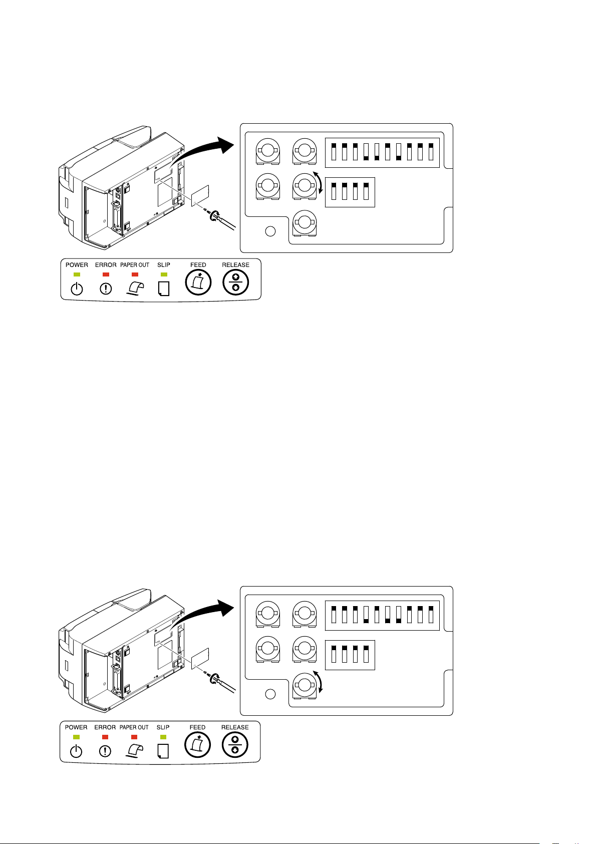
3. Sensor Adjustment
ERR
OR
PAPE
ROU
T
SLI
P
FEED
RE
LEASE
1 2 3 4 5 6 7 8 9
10
1 2 3 4
VR1
VR2
VR3
VR4
VR5
is printer is equipped with the following ve paper sensors:
• PE (Paper End) Sensor
Detects whether a roll paper is loaded on the printer.
• NE (Near End) sensor
Detects whether the roll paper is nearing its end.
• BOF (Bottom of Feed) Sensor
Detects whether a slip paper is placed on the printer.
• COF (Center of Feed) Sensor
Detects the feed position for printing on a slip of paper.
• TOF (Top of Feed) Sensor
Detects the top of feed of a slip paper.
NE Sensor
PE Sensor
COF Sensor
BOF Sensor
e aforementioned sensors can be adjusted as follows.
TOF Sensor
3-1. PE Sensor Adjustment Mode
(1) Make sure the printer power is turned OFF.
(2) Open the rear cover and set a paper roll in place, thus setting the printer in the “paper present” state.
(3) Undo the screws and remove the DIP switch cover from the bottom of the printer.
(4) Using the tip of a ballpoint pen or a similar object, set the DIP switches as follows: DIPSW1-4 OFF, DIPSW1-5 ON,
DIPSW1-6 OFF, DIPSW1-7 and DIPSW1-8 ON. Turn the printer power ON. e lamps on the control panel will ash,
and the printer will enter the sensor adjustment mode.
Using a small slot screwdriver, turn VR1 as shown below, and adjust it so that all the lamps are lit: POWER lamp (green:
(5)
constant ON), ERROR lamp (red), PAPER OUT lamp (red), and SLIP lamp (green).
Turn the printer power OFF, and restore the DIP switches DIPSW1-4, DIPSW1-5, DIPSW1-6, DIPSW1-7, and
(6)
DIPSW1-8 to their original settings.
- 5 -
Page 9
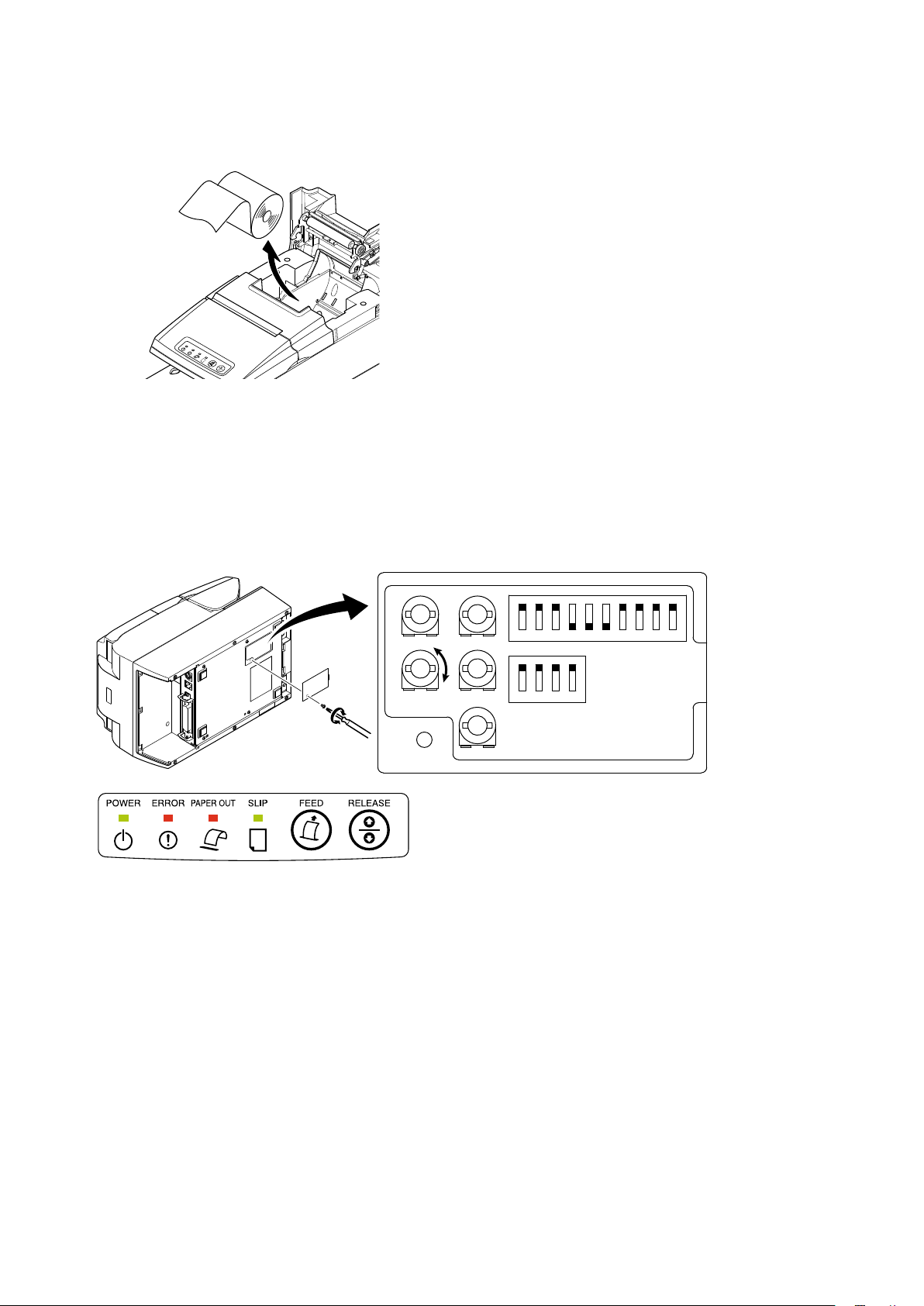
3-2. NE Sensor Adjustment Mode
ERROR
PAPER OUT
SLIP
FEED
RELEASE
1 2 3 4 5 6 7 8 9
10
1 2 3 4
VR1
VR2
VR3
VR4
VR5
(1) Make sure the printer power is turned OFF.
(2) Open the rear cover and remove the paper roll, thus setting the printer in the “paper absent” state.
(3) Undo the screws and remove the DIP switch cover from the bottom of the printer.
(4) Using the tip of a ballpoint pen or a similar object, set the DIP switches as follows: DIPSW1-4, DIPSW1-5 and DIPSW1-6
OFF, and DIPSW1-7 and DIPSW1-8 ON. Turn the printer power ON. e lamps on the control panel will ash, and the
printer will enter the sensor adjustment mode.
(5)
Using a small slot screwdriver, turn VR2 as shown below, and adjust it so that all the lamps are lit: POWER lamp (green:
constant ON), ERROR lamp (red), PAPER OUT lamp (red), and SLIP lamp (green).
Turn the printer power OFF, and restore the DIP switches DIPSW1-4, DIPSW1 -5, DIPSW1-6, DIPSW1-7, and
(6)
DIPSW1-8 to their original settings.
3-3. BOF Sensor Adjustment Mode
(1) Make sure the printer power is turned OFF.
(2) Set the slip slot in the “paper absent” state.
(3) Undo the screws and remove the DIP switch cover from the bottom of the printer.
(4) Using the tip of a ballpoint pen or a similar object, set the DIP switches as follows: DIPSW1-4 OFF, DIPSW1-5 and
DIPSW1-6 ON, DIPSW1-7 OFF, and DIPSW1-8 ON. Turn the printer power ON. e lamps on the control panel will
ash, and the printer will enter the sensor adjustment mode.
- 6 -
Page 10
(5) Using a small slot screwdriver, turn VR3 as shown below, and adjust it so that all the lamps are lit: POWER lamp (green:
1 2 3 4 5 6 7 8 9
10
1 2 3 4
VR1
VR2
VR3
VR4
VR5
POWER
ERROR
PAPEROUT
SLIP
FEED
RELEASE
constant ON), ERROR lamp (red), PAPER OUT lamp (red), and SLIP lamp (green).
Turn the printer power OFF, and restore the DIP switches DIPSW1-4, DIPSW1-5, DIPSW1-6, DIPSW1-7, and
(6)
DIPSW1-8 to their original settings.
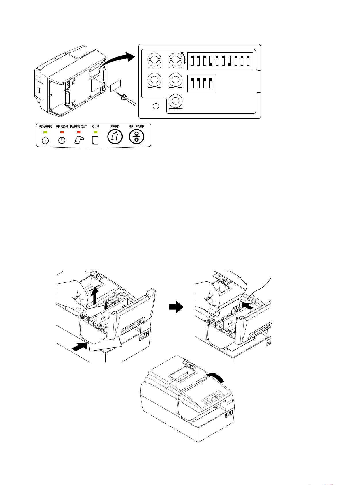
3-4. COF Sensor Adjustment Mode
(1) Make sure the printer power is turned OFF.
(2) Insert a slip paper to set the printer in the “paper present” state.
Note : For sensor adjustment, use a clean, white paper, approximately A6 in size.
To do so, open the front cover as shown below and insert the paper diagonally from the le.Set the paper straight while
pressing on the platen. en, close the front cover.
Undo the screws and remove the DIP switch cover from the bottom of the printer.
(3)
- 7 -
Page 11
(4) Using the tip of a ballpoint pen or a similar object, set the DIP switches as follows: DIPSW1-4 and DIPSW1-5 OFF,
1 2 3 4 5 6 7 8 9
10
1 2 3 4
VR1
VR2
VR3
VR4
VR5
1 2 3 4 5 6 7 8 9
10
1 2 3 4
VR1
VR2
VR3
VR4
VR5
DIPSW1-6 ON, DIPSW1-7 OFF, and DIPSW1-8 ON. Turn the printer power ON. e lamps on the control panel will
ash, and the printer will enter the sensor adjustment mode.
(5)
Using a small slot screwdriver, turn VR4 as shown below, and adjust it so that all the lamps are lit: POWER lamp (green:
constant ON), ERROR lamp (red), PAPER OUT lamp (red), and SLIP lamp (green).
Turn the printer power OFF, and restore the DIP switches DIPSW1-4, DIPSW1-5, DIPSW1-6, DIPSW1-7, and
(6)
DIPSW1-8 to their original settings.
3-5. TOF Sensor Adjustment Mode
(1) Make sure the printer power is turned OFF.
(2) Insert a slip paper to set the printer in the “paper present” state.
Note : For sensor adjustment, use a clean, white paper, approximately A6 in size.
To do so, open the front cover and insert the paper diagonally from the le. Set the paper straight while pressing on the
platen. en, close the front cover.
ee the illustration under “3-4. COF Sensor Adjustment Mode” for instructions on how to set the paper in place.
S
(3) Undo the screws and remove the DIP switch cover from the bottom of the printer.
(4) Using the tip of a ballpoint pen or a similar object, set the DIP switches as follows: DIPSW1-4 OFF, DIPSW1-5 ON,
DIPSW1-6 and DIPSW1-7 OFF, and DIPSW1-8 ON. Turn the printer power ON. e lamps on the control panel will
ash, and the printer will enter the sensor adjustment mode.
Using a small slot screwdriver, turn VR5 as shown below, and adjust it so that all the lamps are lit: POWER lamp (green:
(5)
constant ON), ERROR lamp (red), PAPER OUT lamp (red), and SLIP lamp (green).
Turn the printer power OFF, and restore the DIP switches DIPSW1-4, DIPSW1-5, DIPSW1-6, DIPSW1-7, and
(6)
DIPSW1-8 to their original settings.
- 8 -
Page 12

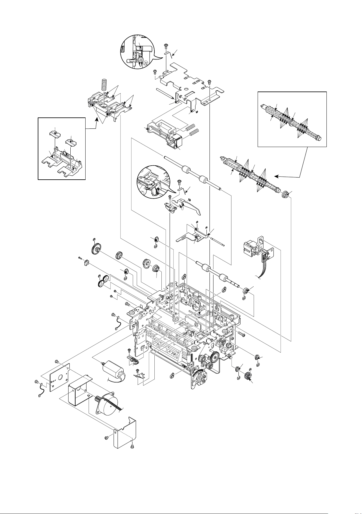
CHAPTER 2
PARTS REPLACEMENT
is chapter explains disassembly and reassembly of the printer. Note the following precautions during disassembly and
reassembly.
1. Disconnect the printer power cord plug from the wall outlet before servicing it.
2. Assembly is the reverse of disassembly unless otherwise specied.
3. Lubrication information is not provided in this chapter. Refer to item 2 of chapter 3.
1. Cover Unit . . . . . . . . . . . . . . . . . . . . . . . . . . . . . . . . . . . . . . . . . . . . . . . . . . . . .10
2. Operation Panel Unit and Upper Case Unit . . . . . . . . . . . . . . . . . . . . . . . .10
3. Board Cover and Interface Board . . . . . . . . . . . . . . . . . . . . . . . . . . . . . . . .11
4. Main Logic Board and Board Chassis . . . . . . . . . . . . . . . . . . . . . . . . . . . . .11
5. Slip Printer Mechanism . . . . . . . . . . . . . . . . . . . . . . . . . . . . . . . . . . . . . . . . .12
6. Frame (E) Unit . . . . . . . . . . . . . . . . . . . . . . . . . . . . . . . . . . . . . . . . . . . . . . . . . .12
7. Thermal Printer Mechanism . . . . . . . . . . . . . . . . . . . . . . . . . . . . . . . . . . . . .13
8. Power Supply Switch Unit and Base . . . . . . . . . . . . . . . . . . . . . . . . . . . . . .13
9. Impact Print Head . . . . . . . . . . . . . . . . . . . . . . . . . . . . . . . . . . . . . . . . . . . . . .14
10. PF Motor . . . . . . . . . . . . . . . . . . . . . . . . . . . . . . . . . . . . . . . . . . . . . . . . . . . . .14
11. DC Moter . . . . . . . . . . . . . . . . . . . . . . . . . . . . . . . . . . . . . . . . . . . . . . . . . . . . .15
12. CR Moter . . . . . . . . . . . . . . . . . . . . . . . . . . . . . . . . . . . . . . . . . . . . . . . . . . . . .15
13.Cutter Unit . . . . . . . . . . . . . . . . . . . . . . . . . . . . . . . . . . . . . . . . . . . . . . . . . . . .16
14. Thermal Print Head . . . . . . . . . . . . . . . . . . . . . . . . . . . . . . . . . . . . . . . . . . . .17
15. MICR Head <HSP7743> . . . . . . . . . . . . . . . . . . . . . . . . . . . . . . . . . . . . . . . .17
16. MICR Head <HSP7643> . . . . . . . . . . . . . . . . . . . . . . . . . . . . . . . . . . . . . . . .18
Page 13
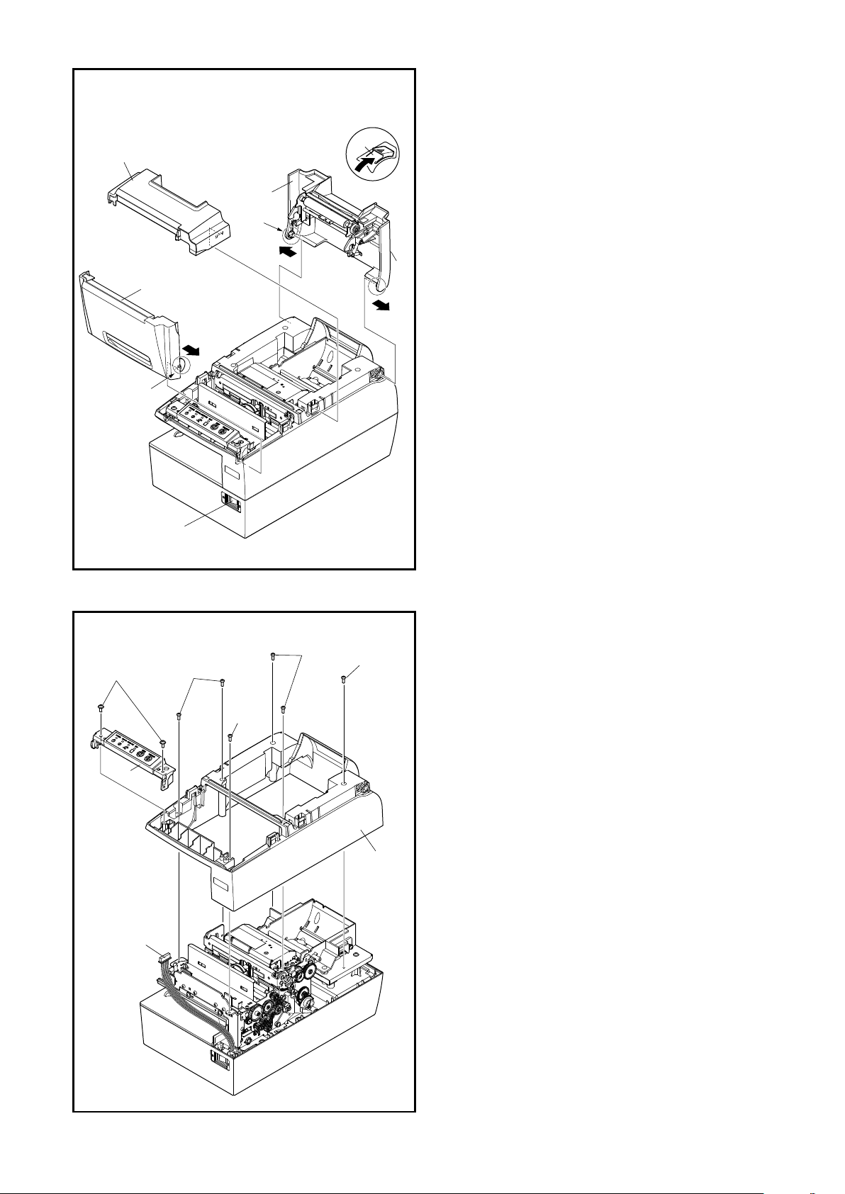
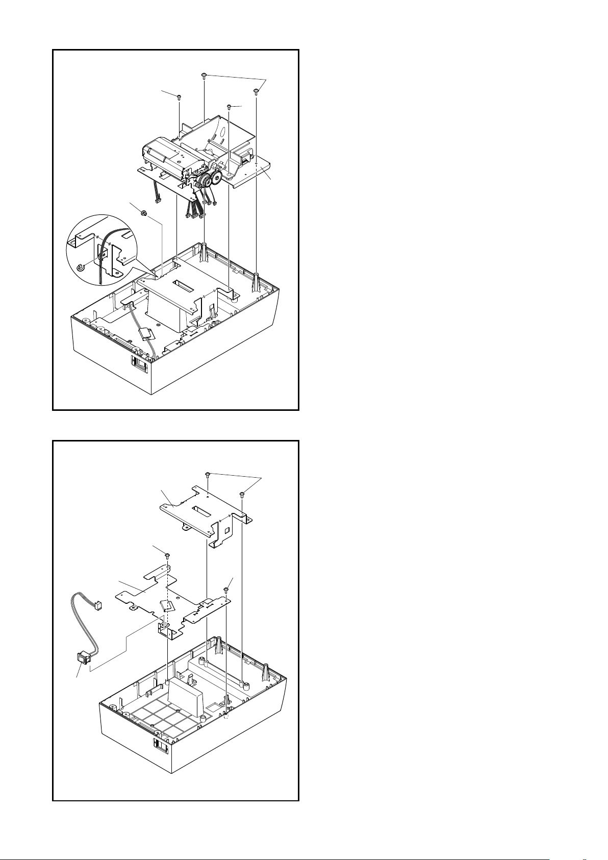
1. Cover Units
A
B
1
4
5
3
2
2
4
4
4
4
1
3
2
5
1. Turn the power switch 1 off and unplug the power
plug from the AC outlet.
2.
Push the open lever 2 and open rear cover unit
Spread to the outside at points A (left/right)of rear
3.
cover 4, and remove rear cover unit.
4.
Open the front cover 4.
S
pread to the outside at points B (left/right) of front
cover, and remove front cover.
Removal
5.
• Cutter cover
5
3
2. Operation Panel Unit and Upper Case Unit
1. Turn the power off and unplug the power plug from
the AC outlet.
2.
Remove the cover units according to the procedure
described in item 1.
3.
Removal
• 2 screws 1
• Connector 2
• Operation panel unit 3
• 6 screws 4
• Upper case unit 5
- 10 -
Page 14
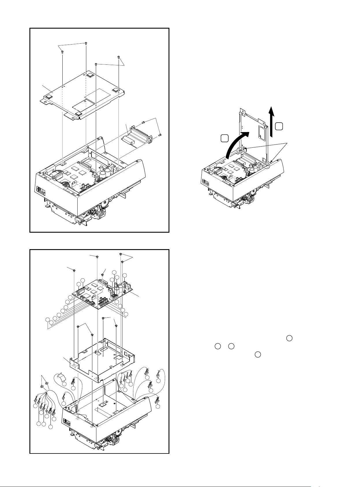
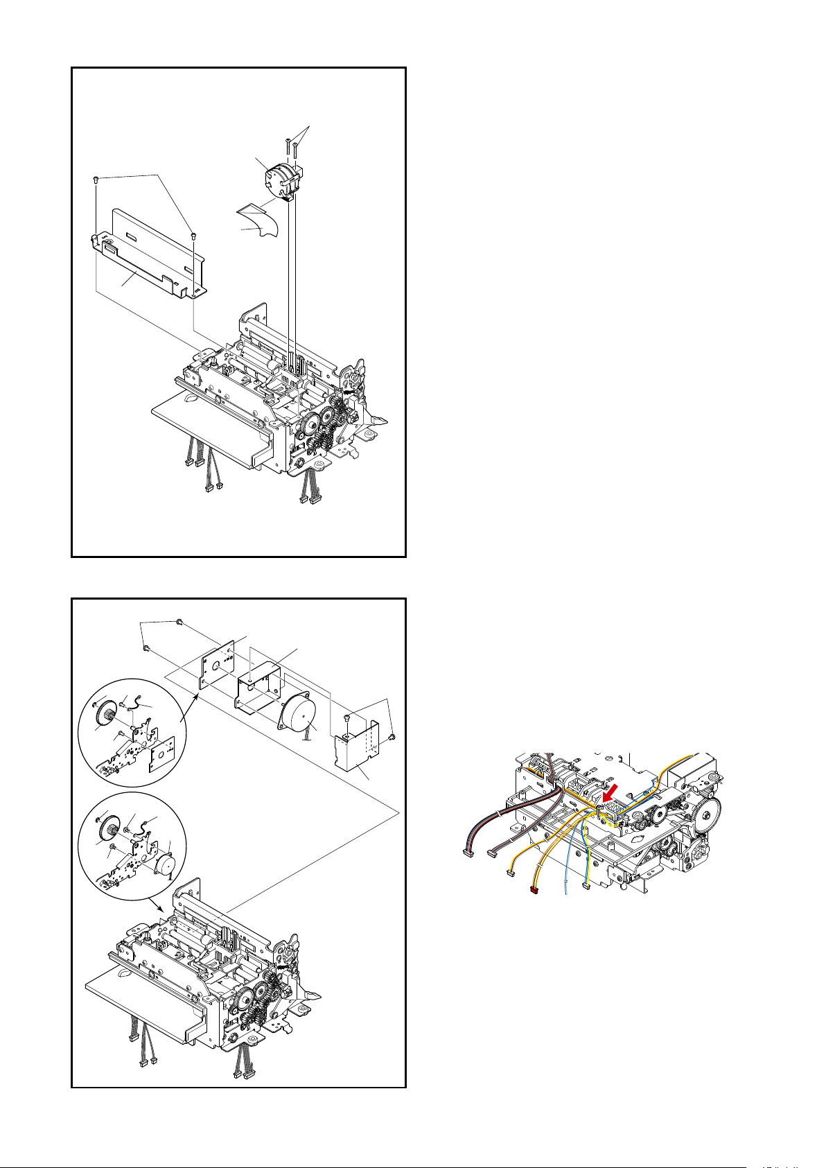
3. Board Cover and Interface Board
1
1
2
3
4
A
B
B
C
C
D
D
E
E
F
F
G
G
H
H
I
I
K
K
L
L
M
M
N
N
O
O
Q
Q
P
P
R
R
J
J
A
1
1
1
1
2
3
4
4
5
1
2
1. Turn the power off and unplug the power plug from
the AC outlet.
2.
Removal
• 4 screws 1
• Board cover 2
ere is a hooks in the backside. li the front side of
board cover to remove board cover.
Hooks
• 2 screws 3
• Interface board 4
4. Main Logic Board and Board Chassis
1. Turn the power off and unplug the power plug from
the AC outlet.
2.
Remove the board cover and interface board according
to the procedure described in item 3.
3.
Cut the 2 fasteners
and remove them from the
2
cable.
Remove the slip printer head cable A and al l
4.
connectors B to R .
*HS
5. Removal
P7543 only doesn't have R .
• 5 screws 1
• Main logic board 3
• 4 screws 4
• Board chassis 5
- 11 -
Page 15
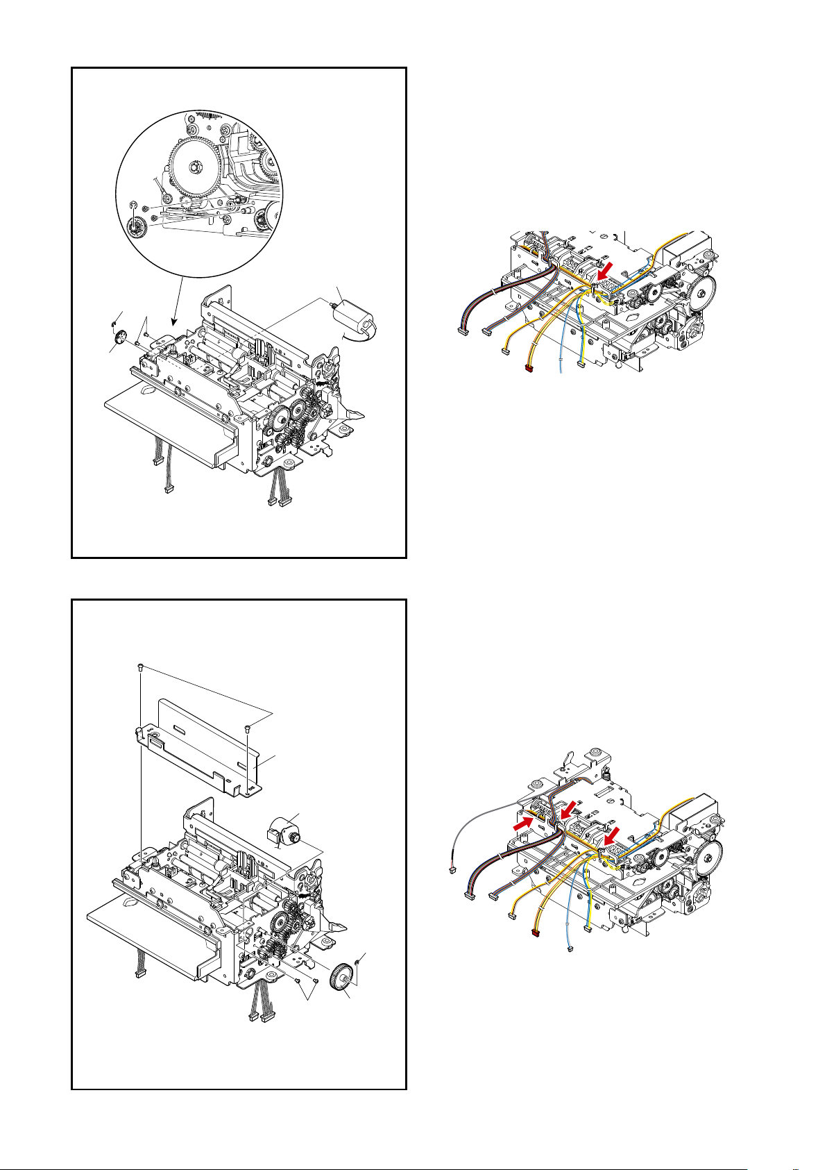
5. Slip Printer Mechanism
1
2
3
2
1
3
3
4
1. Turn the power off and unplug the power plug from
the AC outlet.
2.
Remove the head cable, all connectors and a main
logic board according to the procedure described in
item 4.
Remove screw 1 that is holding the wire in place.
3.
Removal
4.
• 2 screws 2
• 4 screws 3
• Slip printer mechanism 4
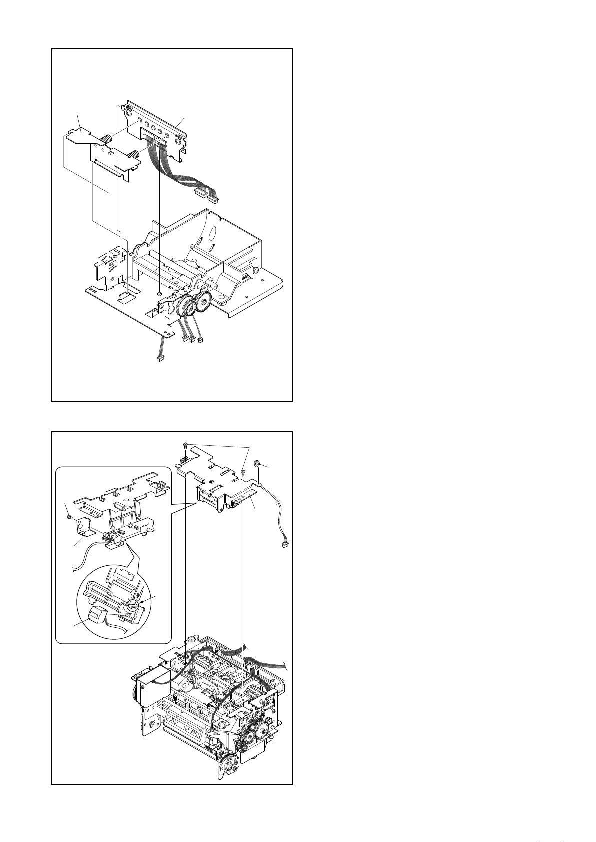
6. Frame (E) Unit
1. Turn the power off and unplug the power plug from
the AC outlet.
2.
Remove the slip printer mechanism to the procedure
described in item 5.
3.
Removal
• Screw 1
• Screw 2
• Frame (E) unit 3
- 12 -
Page 16
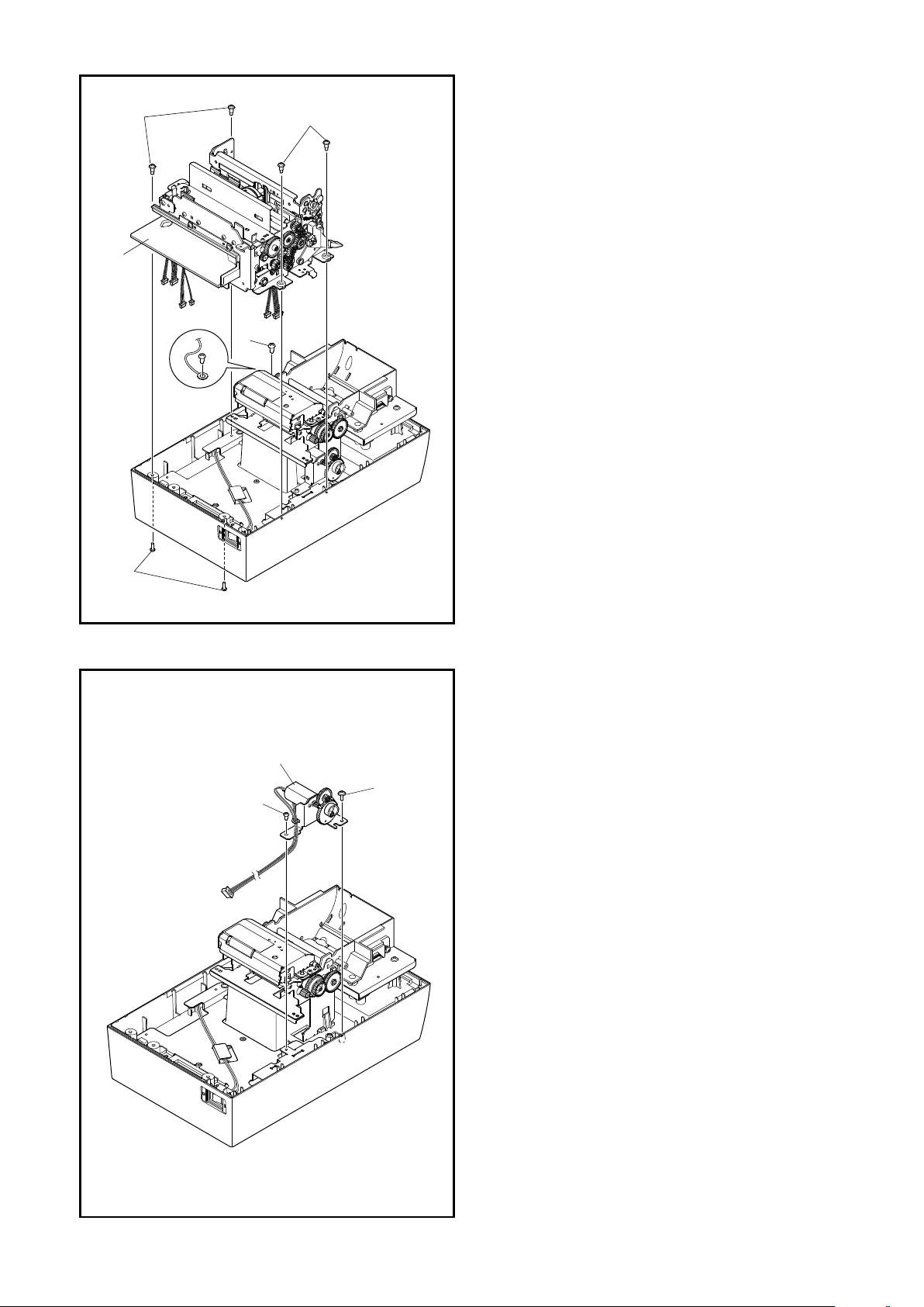
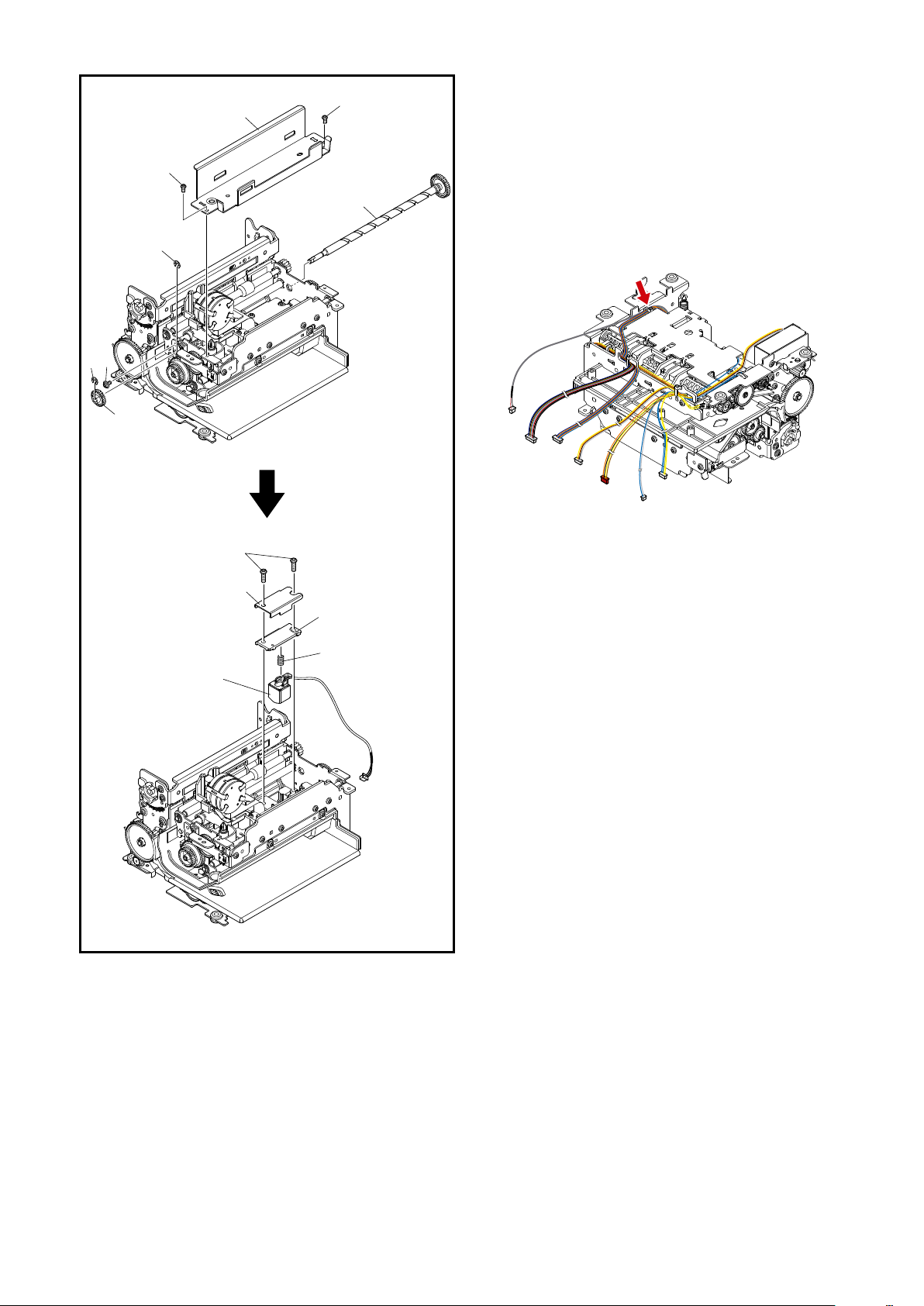
7. Thermal Pinter Mechanism
1
2
2
3
4
1
2
3
4
3
5
1. Turn the power off and unplug the power plug from
the AC outlet.
2.
Remove the frame (E) unit to the procedure described
in item 6.
3.
Removal
• 2 screws 1
• 2 screws 2
• Fastener 3
• ermal printer mechanism
4
8. Power Supply Switch Unit and Bases
1. Turn the power off and unplug the power plug from
the AC outlet.
2.
Remove the thermal printer mechanism to the proce-
dure described in item 7.
3.
Removal
• 2 screws 1
• ermal base 2
• 2 screws 3
• Slip base 4
• Power supply switch unit
5
- 13 -
Page 17
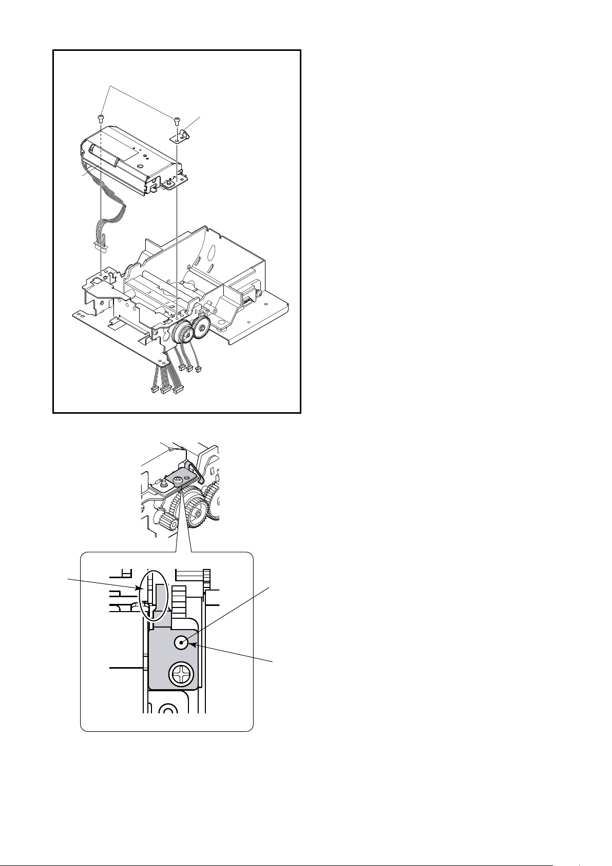
9. Impact Print Head
1
2
3
5
4
1
2
3
3
5
9
1
2
3
3
4
4
8
6
9
7
5
<HSP7643/ 7743>
<HSP7543>
1. Turn the power off and unplug the power plug from
the AC outlet.
2.
Remove the slip printer mechanism to the procedure
described in item 5.
3.
Removal
• 2 screws 1
• Ribbon base 2
• 2 screws 3
• Head cable 4
• Impact print head
Caution in assembly:
e impact print head and the head cable recommend
always be replace at the same time.
5
10. PF Motor
1. Turn the power off and unplug the power plug from
the AC outlet.
2.
Remove the slip printer mechanism to the procedure
described in item 5.
3.
Cut the fastener.
4. Removal
• Stop ring 1
• Gear 2
• 2 screws 3
• 4 screws 4 <HSP7643/7743>
• Wire 5
• PF shield cover A 6 <HSP7643/7743>
• PF shield cover B 7 <HSP7643/7743>
• PF shield cover C 8 <HSP7643/7743>
• PF motor
9
- 14 -
Page 18
11. DC Motor
1
2
3
4
3
4
5
6
1
2
1. Turn the power off and unplug the power plug from
the AC outlet.
2.
Remove the slip printer mechanism to the procedure
described in item 5.
3.
Cut the fastener.
4. Removal
• Stop ring 1
• Gear 2
• 2 screws 3
• DC motor 4
12. CR Motor
1. Turn the power off and unplug the power plug from
the AC outlet.
2.
Remove the slip printer mechanism to the procedure
described in item 5.
Cut the 3 fasteners.
3.
4. Removal
• 2 screws 1
• Ribbon base 2
• Stop ring 3
• Gear 4
• 2 screws 5
• CR motor 6
- 15 -
Page 19
13. Cutter Unit
1
2
3
C
1. Turn the power off and unplug the power plug from
the AC outlet.
2.
Remove the thermal printer mechanism to the proce-
dure described in item 7.
3.
Removal
• 2 screws 1
• Holder spring 2
• Cutter unit 3
Caution in assembly:
e cutter unit and the platen holder unit must always
be replace at the same time.
Aer assembling, always apply grease to the holder
spring. (See Chapter3 3-2. Lubrication Locations for
details such as the locations for applying lubrication.)
Also, when installing the holder spring, be careful of
the following. (See the drawings at le.)
-
Be careful that the holder spring does not turn
along when tightening with the screw. It should
be mounted straight.
- Look from above the printer after tightening with
a screw to check that the half-cut of the frame is
securely in the hole in the holder spring.
- Check that there is adequate clearance (the area
of C) between the frame and the holder spring.
half-cut of the frame
hole in the holder spring
- 16 -
Page 20
14. Thermal Print Head
1
2
1
2
4
5
6
3
A
1. Turn the power off and unplug the power plug from
the AC outlet.
2.
Remove the cutter unit to the procedure described in
item 13.
3.
Removal
• Spring holder unit 1
• ermal print head 2
15. MICR Head <HSP7743>
1. Turn the power off and unplug the power plug from
the AC outlet.
2.
Remove the slip printer mechanism to the procedure
described in item 5.
3.
Remove the 2 screws 1 to remove the frame (D) unit 2.
4.
Cut and remove the fastener 3 that is holding the
MICR head cable in place.
5.
Removal
• Screw 4
• MICR shield cover A 5
• MICR head B 6
T
o facilitate the removal of the MICR head, open the
hook in points A outward.
- 17 -
Page 21
16. MICR Head <HSP7643>
8
9
0
A
B
1
1
7
6
3
5
4
2
1. Turn the power off and unplug the power plug from
the AC outlet.
2.
Remove the slip printer mechanism to the procedure
described in item 5.
3.
Cut and remove the fastener that is holding the MICR
head cable in place.
4.
Removal
• 2 screws 1
• Ribbon base 2
• Stop ring 3
• Drive sha gear 4
• Screw 5
• Stop ring 6
• Drive sha 7
• 2 screws 8
• MICR shield cover C 9
• Spring holder 0
• Spring A
• MI
CR head U
B
- 18 -
Page 22

CHAPTER 3
MAINTENANCE AND LUBRICATION
1. Maintenance . . . . . . . . . . . . . . . . . . . . . . . . . . . . . . . . . . . . . . . . . . . . . . . . 20
1-1. Cleaning . . . . . . . . . . . . . . . . . . . . . . . . . . . . . . . . . . . . . . . . . . . . . . . . . . .20
1-2. Checks . . . . . . . . . . . . . . . . . . . . . . . . . . . . . . . . . . . . . . . . . . . . . . . . . . . . .20
2. Lubrication . . . . . . . . . . . . . . . . . . . . . . . . . . . . . . . . . . . . . . . . . . . . . . . . . 20
2-1. Lubricant . . . . . . . . . . . . . . . . . . . . . . . . . . . . . . . . . . . . . . . . . . . . . . . . . . 20
2-2. Lubricating Method . . . . . . . . . . . . . . . . . . . . . . . . . . . . . . . . . . . . . . . . . 21
2-3. Lubricated Areas . . . . . . . . . . . . . . . . . . . . . . . . . . . . . . . . . . . . . . . . . . . 21
Page 23

1. Maintenance
- 20 -
1-1. Cleaning
(1) Removal of dirt
To remove dirt from the surface of the platen of the thermal printer and the slip printer, gently wipe them with a
dry, so cloth. To remove dirt from other areas, use a so cloth or a cotton swab moistened with alcohol (ethanol/
methanol).
Note: Do not use thinner, trichlene or ketone solvents because they may damage plastic parts.
Also during cleaning, be careful not to moisten or damage electronic parts, wiring, or mechanical parts.
Removal of dust, pile
(2)
Vacuum cleaning (with an electric cleaner) is preferred. Remove all dust, etc., inside the printer.
Note: Aer cleaning, check the oil level. If it is not adequate due to cleaning, replenish it.
1-2. Checks
Checks must be carried out at two levels: “a daily check” which the operator can easily carry out during operation, and a
“periodic check” which an expert should carry out.
Daily check
(1)
When the printer is used on a daily basis, check that the printer is used properly. Make sure that the printer is
perating under the best conditions.
• Is the cartridge ribbon set at the right position?
• Is there any foreign matter inside the printer? (Remove if any.)
• Is the peper set correctly?
(2)
Periodic check
Aer 6 months or printing 1 million lines, the periodic check and lubrication must be carried out.
• Check for deformation of springs.
• Remove any debris, dust, paper particles, or glue from the rubber rollers, paper tray, paper guide, and sensors.
• Remove dirt around the drive sha and lubricate.
• Check the gap between the platen and the impact print head.
2. Lubrication
Lubrication is very important to maintain optimum performance and to prevent trouble.
2-1. Lubricant
e type of lubricant greatly aects the performance and durability of the printer, especially in a low temperature
environment. We recommend use of the grease and lubrication oils listed below for this printer.
Type of oil Product name Maker
Grease Molykote EM-30L Dow Corning Corporation
Grease Isoex NBU-15 NOK Klüber Co., Ltd.
Grease FLOIL G347CA Kanto Kasei Co., Ltd.
Grease Sankol CFD-5007Z Sankei Kagaku Co., Ltd.
Lubricant Mobil 1 Mobil Oil Co., Ltd.
2-2. Lubricating Method
When lubrication is carried out in assembly and disassembly, wash parts well to remove dust and dirt before lubrication.
Lubrication must be carried out regularly once every 6 months or aer 1 million lines have been printed. Lubrication is
necessary irrespective of the regular lubrication whenever lubricant becomes decient aer cleaning or whenever parts
have been disassembled or replaced.
Page 24

2-3. Lubricated Areas
Refer to Fig. 3-1~3-7
No. Lubricating Point Grease/Oil Reference
Rubbing surfaces of Release lever, Platen frame R and Paper feed sha Molykote EM-30L g. 3-1,3-3,3-5
1
Rubbing surfaces of Rear slider and Carriage guide stay FLOIL G347CA g. 3-1,3-3,3-5
2
Rubbing surfaces of Drive sha bearing and Drive sha Molykote EM-30L g. 3-1,3-3,3-5
3
Whole area of drive sha grooves Isoex NBU-15 g. 3-1,3-3,3-5
4
Rubbing surfaces of Ribbon sha, Worm wheel and Frame C Molykote EM-30L g. 3-1,3-3,3-5
5
Rubbing surfaces of Worm gear sha and Worm gear Molykote EM-30L g. 3-1,3-3,3-5
6
Rubbing surfaces of Worm gear and Frame C Molykote EM-30L g. 3-1,3-3,3-5
7
Rubbing surfaces of Worm gear and Worm wheel Molykote EM-30L g. 3-1,3-3,3-5
8
Rubbing surfaces of Frame unit L-U and Worm gear Molykote EM-30L g. 3-1,3-3,3-5
9
Rubbing surfaces of Ribbon sha unit and Back stop spring Molykote EM-30L g. 3-1,3-3,3-5
0
Rubbing surfaces of Ribbon sha unit and Ribbon base Molykote EM-30L g. 3-1,3-3,3-5
A
Rubbing surfaces of Bushing B and Paper feed roller B Molykote EM-30L g. 3-2,3-4,3-6
B
Rubbing surfaces of Shutter access plate and Sha B Molykote EM-30L g. 3-2,3-4,3-6
C
Rubbing surfaces of Shutter access plate and Cam sha Molykote EM-30L g. 3-2,3-4,3-6
D
Rubbing surfaces of Bushing F7 x 10 x 6 and Cam sha Molykote EM-30L g. 3-2,3-4,3-6
E
Rubbing surfaces of Gear sha of frame unit L-B and Gear Molykote EM-30L g. 3-1,3-3,3-5
F
Rubbing surfaces of Roller holder, frame A and MICR holder Molykote EM-30L g. 3-2,3-4,3-6
G
Rubbing surfaces of Roller holder and Paper feed roller B Molykote EM-30L g. 3-2,3-4,3-6
H
Rubbing surfaces of Roller holder and Cam sha Molykote EM-30L g. 3-2,3-6
I
Rubbing surfaces of Paper feed roller B and Roller ground spring Molykote EM-30L g. 3-2,3-4,3-6
J
Rubbing surfaces of Gear sha of frame R and Gear Molykote EM-30L g. 3-1,3-3,3-5
K
Rubbing surfaces of Gear sha A of frame unit L-B and Paper feed roller D Molykote EM-30L g. 3-1,3-3,3-5
L
Rubbing surfaces of Gear sha E of frame unit L-U and Gear 32 x 48 x 0.5 Molykote EM-30L g. 3-1,3-3,3-5
M
Felt and Carriage stay Mobil 1 g. 3-1,3-3,3-5
N
Rubbing surfaces of Locating lever and sha D of Locating lever holder Molykote EM-30L g. 3-2,3-4,3-6
O
Rubbing surfaces of Frame D and Sha C Molykote EM-30L g. 3-2,3-4,3-6
P
Rubbing surfaces of Cam sha and Frame A Molykote EM-30L g. 3-2,3-4,3-6
Q
Rubbing surfaces of Paper guide A and Paper feed roller J Molykote EM-30L g. 3-1,3-3,3-5
R
Rubbing surfaces of Paper feed roller J and Bushing C Molykote EM-30L g. 3-1,3-3,3-5
S
Rubbing surfaces of Holder springs and Platen holder Molykote EM-30L g. 3-7
T
Rubbing surfaces of Gear sha A and Gear 22 x 46 x 0.5 Molykote EM-30L g. 3-7
U
Rubbing surfaces of Gear sha B and Gear 32 x 48 x 0.5 Molykote EM-30L g. 3-7
V
Rubbing surfaces of Gear 32 x 48 x 0.5 and Gear 22 x 46 x 0.5 Molykote EM-30L g. 3-7
W
Rubbing surfaces of Gear 32 x 48 x 0.5 and Pinion 14 x 0.5 Molykote EM-30L g. 3-7
X
Rubbing surfaces of Assistance roller and Paper guide Molykote EM-30L g. 3-7
Y
Whole surfaces of Paper feed gear E, Paper feed gear D,
Z
Paper feed roller gear B and Paper feed gear C
Rubbing surfaces of Bushing B, Paper feed roler D and Paper feed roler I Molykote EM-30L g. 3-4,3-6
[
Rubbing surfaces of Paper feed roler D, Paper feed roler I and Roller ground spring Molykote EM-30L g. 3-4,3-6
\
Rubbing surfaces of MICR holder A, Paper feed roller D and Paper feed roller I Molykote EM-30L g. 3-4,3-6
]
Rubbing surfaces of Roller holder and Protect plate Molykote EM-30L g. 3-4
^
Rubbing surfaces of Protect plate and Cam sha Molykote EM-30L g. 3-4
a
Rubbing surfaces of Gear sha of Gear plate unit and Paper feed roller gear B Molykote EM-30L g. 3-4
b
Rubbing surfaces of Paper feed roller D, Gear sha of Gear plate unit and
c
Paper feed sub-roller
Rubbing surfaces of Release lever and Cam gear B of Frame E unit Molykote EM-30L g. 3-1,3-3,3-5
d
Note: I
^abc
are only for HSP7743 model and HSP7543 model,
are only for HSP7643 model
[\]
are only for HSP7643 model and HSP7543 model,
Sankol CFD-5007Z
Molykote EM-30L g. 3-3,3-4
g. 3-1,3-3,
3-5,3-6
- 21 -
Page 25

D
E
F
C
G
H
B
A
D
E
F
C
G
H
B
A
I
J
K
L
I
J
K
L
< FRAME E >
5
8
0
9
5
6
8
7
1
1
Z
Z
Z
Z
Z
Z
1
2
2
4
4
3
2
A
F
L
K
S
S
R
N
N
M
5
5
d
- 22 -
Fig.3-1. Lubricated Area : In Slip Printer Mechanism Unit-1 ( for HSP7743 1/2 )
Page 26
B
B
C
C
D
E
E
G
G
G
H
I
D
D
I
O
Q
Q
P
P
I
I
I
I
I
I
I
D
D
Q
I
J
J
Fig.3-2. Lubricated Area : In Slip Printer Mechanism Unit-2 ( for HSP7743 2/2 )
- 23 -
Page 27
c
c
D
E
F
C
G
H
B
A
D
E
F
C
M
M
G
H
B
A
I
J
L
I
J
L
5
8
0
9
5
6
8
7
1
1
Z
d
Z
Z
b
Z
Z
Z
Z
1
2
2
4
4
3
2
A
F
L
K
S
S
R
N
N
M
5
5
< FRAME E >
- 24 -
Fig.3-3. Lubricated Area : In Slip Printer Mechanism Unit-3 ( for HSP7643 1/2 )
Page 28
B
]
[
B
[
C
C
c
D
]
E
E
G
G
G
H
a
^
a
D
D
D
D
a
^
J
J
\
\
O
Q
Q
Q
P
P
a
a
a
a
a
a
a
Z
Fig.3-4. Lubricated Area : In Slip Printer Mechanism Unit-4 ( for HSP7643 2/2 )
- 25 -
Page 29

D
E
F
C
G
H
B
A
D
E
F
C
G
H
B
A
I
J
K
L
I
J
K
L
< FRAME E >
5
8
0
9
5
6
8
7
1
1
Z
Z
Z
Z
Z
Z
1
2
2
4
4
3
2
A
F
L
K
S
S
R
N
N
M
5
5
d
- 26 -
Fig.3-5. Lubricated Area : In Slip Printer Mechanism Unit-5 ( for HSP7543 1/2 )
Page 30

B
]
[
B
[
C
C
D
]
E
E
G
G
G
H
I
I
D
D
D
D
I
J
J
\
\
O
Q
Q
Q
P
P
I
I
I
I
I
I
I
Fig.3-6. Lubricated Area : In Slip Printer Mechanism Unit-6 ( for HSP7543 2/2 )
- 27 -
Page 31

Y
V
T
T
W
X
U
Fig.3-7. Lubricated Area : In Thermal Printer Mechanism Unit ( for all models )
- 28 -
Page 32

CHAPTER 4 PARTS LIST
HOW TO USE PARTS LIST
(1) DRWG. NO.
is column shows the drawing number of the illustration.
(2) REVISED EDITION MARK
is column shows a revision number.
Part that have been added in the revised edition are indicated with “#”.
Part that have been abolished in the revised edition are indicated with “*”.
#1 : First edition → Second edition *1 : First edition → Second editon
#2 : Second edition → ird edition *2 : Second edition → ird editon
(3) PART NO.
Parts numbers must be notied when ordering replacement parts. Parts described as “NPN” have no parts number
and are not in stock, i.e., unavailable.
(4) PARTS NAME
Parts names must be notied when ordering replacement parts.
(5) Q’TY
is column shows the number of the part used as indicated in the gure.
(6) REMARKS
hen dierences in specications exist depending on location/destination.
W
(7) RANK
arts marked “S” in the rank column can be ordered. Other parts, as a rule, cannot be supplied even if ordered.
P
Parts marked “O” are optional parts.
1. Printer Assembly........................30
1-1. Disassembly Drawing ...........30
1-2. Parts List ................................ 31
2. Slip Printer Mechanism .............33
2-1. Disassembly Drawing ...........33
2-2. Parts List ................................ 39
3. Thermal Printer Mechanism ......42
3-1. Disassembly Drawing ...........42
3-2. Parts List ................................ 43
4. Sub-Assembly ............................44
4-1. Rear Cover Unit .....................44
4-2. Frame Unit L-B ......................45
Thermal Head Unit ................46
4-3.
5. Block Diagram ............................47
6. Main Logic Board .......................48
6-1. Circuit Diagram .....................48
6-2. Component Layout ...............59
Parts List ................................ 60
6-3.
8. Serial Interface Board ................69
8-1. Circuit Diagram .....................69
8-2. Parts List ................................ 70
9. Parallel Interface Board .............71
9-1. Circuit Diagram .....................71
9-2. Parts List ................................ 72
10. USB Interface Board ..................73
10-1. Circuit Diagram .....................73
10-2. Component Layout ...............74
Parts List ................................ 75
10-3.
11. Ethernet Interface Board ...........76
11-1. Circuit Diagram .....................76
11-2. Component Layout ...............81
1-3. Parts List ................................82
1
12. PoweredUSB Interface Board ....85
12-1. Circuit Diagram .....................85
12-2. Component Layout ...............86
Parts List ................................ 87
12-3.
7. Operation Panel Board ..............68
7-1. Circuit Diagram .....................68
7-2. Parts List ................................ 68
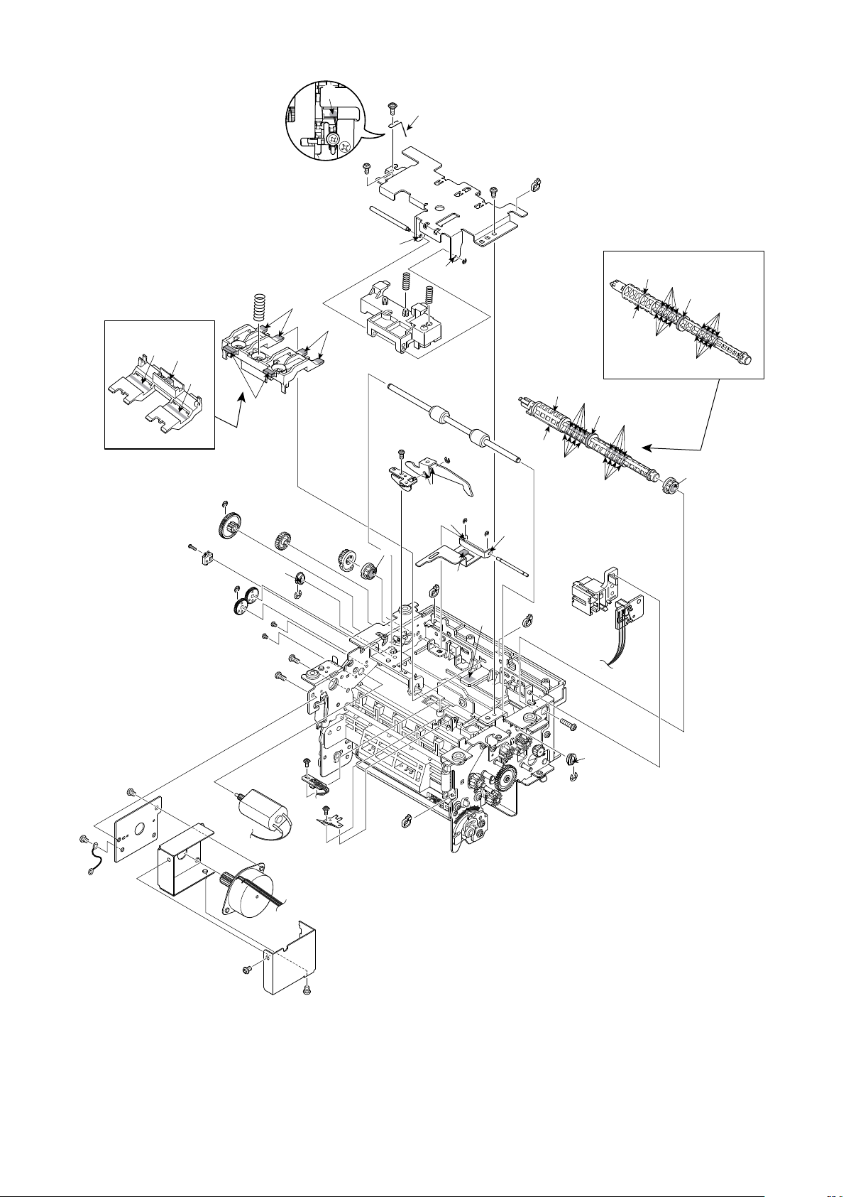
Page 33

POWER
ERROR
PAPER OUT
SLIP
FEED
RELEASE
3
8
7
26
26
26
11
12
23
19
1
27
23
23
23
15
22
21
14
30
9
5
18
32
25
25
16
24
6
24
24
17
17
13
17
17
20
28
27
27
24
24
24
24
10
27
33
22
27
23
23
29
27
2
4
19
26
23
35
27
31
22
34
1. Printer Assembly
1-1. Disassembly Drawing
- 30 -
Page 34

1-2. Parts List
Printer Assembly
DRWG. NO. REV. PARTS NO. PARTS NAME Q'TY REMARKS RANK
1 *3 37628020 SLIP MECHANISM UNIT HSP77 1 HSP7743
#3 37628021 SLIP MECHANISM UNIT HSP77 1 HSP7743 S
*3 37618040 SLIP MECHANISM UNIT HSP75 1 HSP7543
#3 37618041 SLIP MECHANISM UNIT HSP75 1 HSP7543 S
*3 37628050 SLIP MECHANISM UNIT HSP76 1 HSP7643
#3 37628051 SLIP MECHANISM UNIT HSP76 1 HSP7643 S
2 37628000 THERMAL MECHANISM UNIT HSP70 1 S
3 37621200 REAR COVER UNIT HSP70GRY 1 GRAY S
37621210 REAR COVER UNIT HSP70 1 WHITE S
4 37620040 FRAME UNIT E HSP70 1 S
5 37618000 POWER SUPPLY SWITCH UNIT HSP70 1 HSP7543/7743 S
*3 37618020 POWER SUPPLY SWITCH UNIT HSP70 1 HSP7643
#3 37618021 POWER SUPPLY SWITCH UNIT HSP70 1 HSP7643 S
6 *3 37617000 MAIN LOGIC BD UNIT HSP70 1 HSP7643/7743
#3 37617001 MAIN LOGIC BD UNIT HSP70 1 HSP7643/7743 S
*3 37617010 MAIN LOGIC BD UNIT HSP75 1 HSP7543
#3 37617011 MAIN LOGIC BD UNIT HSP75 1 HSP7543 S
7 37611100 OPERATION PANEL UNIT HSP70GRY 1 GRAY S
37611110 OPERATION PANEL UNIT HSP70 1 WHITE S
8 37611000 UPPER CASE UNIT HSP70GRY 1 GRAY S
37611010 UPPER CASE UNIT HSP70 1 WHITE S
9 37610000 LOWER CASE UNIT HSP70GRY 1 GRAY S
37610010 LOWER CASE UNIT HSP70 1 WHITE S
10 39607400 INTERFACE BOARD IFBD-HD04 1 OPTION: SERIAL IF O
39607411 INTERFACE BOARD IFBD-HC04 1 OPTION: PARALLEL IF O
39607602 INTERFACE BOARD IFBD-HE06 1 OPTION: ETHERNET O
39607610 INTERFACE BOARD IFBD-HU06 1 OPTION: USB O
39607700 INTERFACE BOARD IFBD-HPU04 1 OPTION: POWERED USB O
11 33022540 CUTTER COVER HSP70GRY 1 GRAY S
33022610 CUTTER COVER HSP70 1 WHITE S
12 33022530 FRONT COVER HSP70GRY 1 GRAY S
33022600 FRONT COVER HSP70 1 WHITE S
13 NPN BOARD COVER HSP70 1
14 NPN SLIP BASE HSP70 1
15 NPN THERMAL BASE HSP70 1
16 NPN BOARD CHASSIS HSP70 1
17 NPN RUBBER FOOT 12X12 TSP7 4
18 30723010 CABLE UNIT 7X220CC HSP70 1 S
19 30250010 SCREW 3.0 SP2 4 S
20 NPN SWITCH COVER TSP6 1
21 NPN FERRITE CORE BP53-19-12-8 1
22 04991204 FASTENER T18S 5 S
23 01953013 SCREW TAT 3-8 BT-FL 9 S
24 01903101 SCREW TAT 3-6 CT-FL 9 S
25 00930803 SCREW TAT 3-8 PT 2 S
26 00930800 SCREW TAT 3-8 CT 6 S
27 00930609 SCREW TAT 3-6 CT 9 S
28 00930403 SCREW TAT 3-4 CT 1 S
29 33914140 ROLL PAPER GUIDE HSP70 1 S
30 NPN IF COVER ST HSP70GRY 1 GRAY
NPN IF COVER ST HSP70 1 WHITE
31 30970040 THERMAL ROLL PAPER 80X35D 1 S
32 30030030 SWITCH BLIND TSP7GRY 1 GRAY S
30030000 SWITCH BLIND TSP7 1 WHITE S
- 31 -
Page 35

Printer Assembly
DRWG. NO. REV. PARTS NO. PARTS NAME Q'TY REMARKS RANK
33 NPN FERRITE CORE K5BRC24X14X11 2
34 *2 30781573 ADAPTER SET PS60A-24A US 1 OPTION O
*2 30781583 ADAPTER SET PS60A-24A EU 1 OPTION O
*2 30781593 ADAPTER SET PS60A-24A UK 1 OPTION O
*2 30781603 ADAPTER SET PS60A-24A AS 1 OPTION O
#2 30781750 ADAPTER SET PS60A-24B US 1 OPTION O
#2 30781760 ADAPTER SET PS60A-24B EU 1 OPTION O
#2 30781770 ADAPTER SET PS60A-24B UK 1 OPTION O
#2 30781780 ADAPTER SET PS60A-24B AS 1 OPTION O
35 30981300 INK RIBBON CARTRIDGE RC-7KB 1 OPTION O
30981320 INK RIBBON CARTRIDGE RC-7KB 1 OPTION: PLAIN BOX PACKING O
36 #1 NPN PAPER SET SEAL A HSP70 1 HSP7743 ONLY
#2 NPN PAPER SET SEAL B HSP70 1 HSP7643 ONLY
- 32 -
Page 36

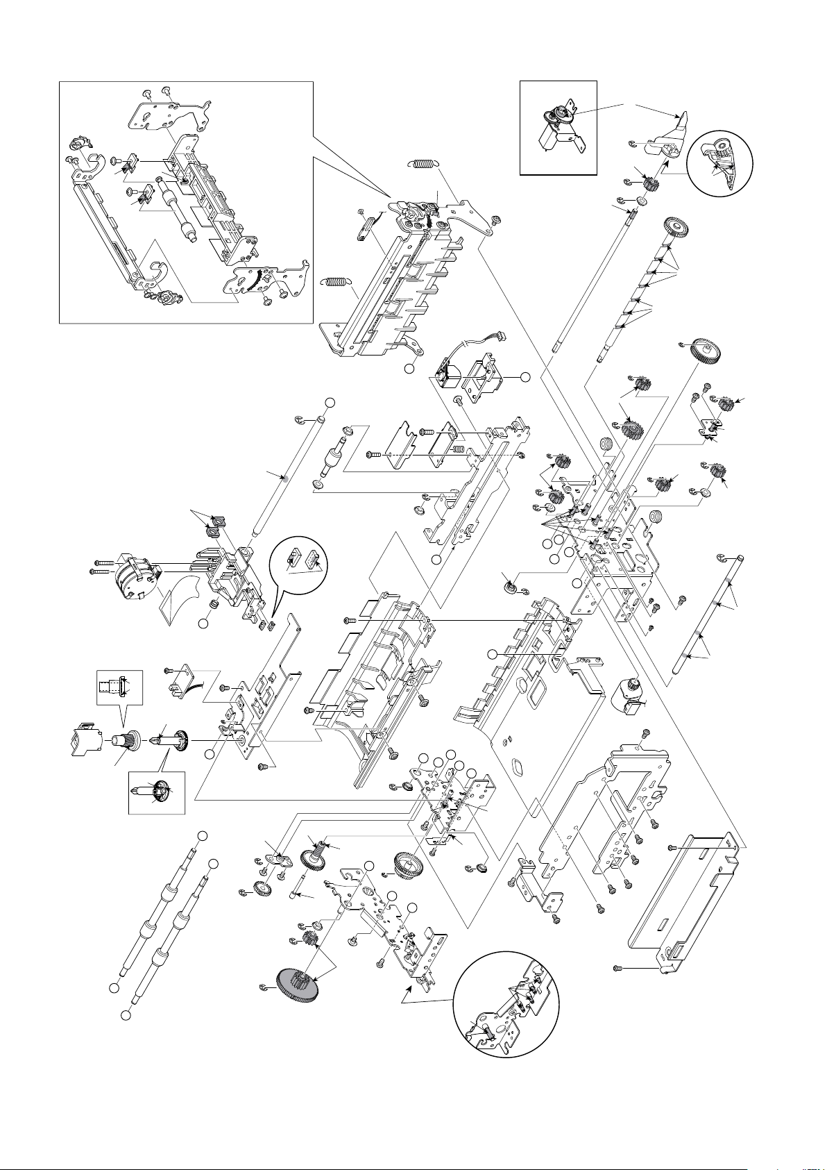
80
59
84
84
70
25
27
54
15
60
5
46
85
4
6
74
8
41
67
70
70
28
39
73
32
33
31
31
87
27
28
72
72
77
82
89
57
89
10
7
9
43
70
86
88
3
58
73
82
2
a
a
b
c
c
d
d
e
70
2. Silp Printer Mechanism
2-1. Disassembly Drawing
2-1-1. HSP7743 (1/2)
- 33 -
Page 37

81
e
*1) If the mechanism you are using is the old type one
which the last digit in its par t number is "0", please
do not use the No.108 spare part which is shown in
the illustration.
D
E
G
L
C
H
I
B
A
D
E
G
F
C
H
I
B
A
J
K
L
M
J
K
L
M
b
e
78
13
24
23
85
63
20
84
84
72
72
72
72
36
64
64
65
68
62
62
1
56
61
74
48
64
72
40
35
80
80
72
84
63
73
84
26
55
29
44
37
18
50
85
85
47
84
84
84
84
84
11
72
64
72
72
72
72
37
37
37
16
85
19
76
22
84
84
83
45
72
64
66
49
75
42
21
64
64
17
17
52
84
84
87
73
30
73
12
51
72
71
72
37
64
69
53
71
38
34
84
84
90
30
73
30
73
72
81
108
(*1)
14
HSP7743 (2/2)
- 34 -
Page 38

41
58
c
80
59
80
59
84
84
103
70
25
27
54
97
60
5
102
46
85
4
6
74
8
67
70
72
70
106
28
28
39
73
32
33
31
31
87
27
28
72
72
72
72
77
82
89
57
89
10
7
9
43
70
86
88
3
28
72
100
72
100
73
82
2
a
a
b
c
d
d
e
73
84
96
30
37
70
2-1-2. HSP7643 (1/2)
- 35 -
Page 39

81
e
*1) If the mechanism you are using is the old type one
which the last digit in its par t number is "0", please
do not use the No.108 spare part which is shown in
the illustration.
D
E
G
L
C
H
I
B
A
D
E
G
F
C
H
I
B
A
J
K
M
J
K
M
b
L
L
e
78
13
24
23
85
63
20
84
84
72
72
72
72
36
64
64
65
68
62
1
56
61
74
48
64
72
40
35
80
80
72
84
63
73
84
26
55
29
44
37
18
50
85
85
47
84
84
84
84
84
11
72
64
72
37
37
16
85
19
76
22
84
83
72
64
105
49
75
42
21
64
17
17
52
84
84
87
73
30
73
12
51
72
71
72
37
64
69
53
71
38
34
107
104
107
84
84
90
30
73
30
73
72
72
64
98
99
95
101
81
108
(*1)
14
62
HSP7643 (2/2)
- 36 -
Page 40

80
59
80
59
84
84
70
25
27
54
92
60
93
93
5
46
85
4
6
74
41
67
70
70
28
28
39
73
32
33
31
91
31
87
27
28
72
72
77
82
57
7
43
70
88
3
28
72
94
70
73
82
2
a
a
b
c
c
d
d
e
2-1-3. HSP7543 (1/2)
- 37 -
Page 41

81
e
*1) If the mechanism you are using is the old type one
which the last digit in its par t number is "0", please
do not use the No.108 spare part which is shown in
the illustration.
D
E
G
L
C
H
I
B
A
D
E
G
F
C
H
I
B
A
J
K
L
M
J
K
L
M
b
e
78
13
24
23
85
63
20
84
84
72
72
72
72
36
64
64
65
68
62
1
56
61
74
48
64
72
40
35
80
80
72
84
63
73
84
26
55
29
44
37
18
50
85
85
47
84
84
84
84
84
11
72
64
72
72
72
72
37
37
37
16
85
19
76
22
84
83
72
64
66
49
75
42
21
64
64
17
17
52
84
84
87
73
30
73
12
51
72
71
72
37
64
69
53
71
38
34
84
84
90
30
73
30
73
72
81
108
(*1)
14
62
HSP7543 (2/2)
- 38 -
Page 42

2-2. Parts List
Slip Printer Mechanism
DRWG. NO. REV. PARTS NO. PARTS NAME Q'TY REMARKS RANK
1 89138030 PRINT HEAD DP1401H HSP70 1 S
2 *3 37627010 DETECTOR UNIT B HSP70 1
#3 37627011 DETECTOR UNIT B HSP70 1 S
3 37627000 DETECTOR UNIT A HSP70 1 S
4 37623010 LOCAT.LEVER HOLDER UNIT HSP70 1 S
5 37623000 ROLLER HOLDER UNIT HSP70 1 S
6 37622020 DC MOTOR UNIT HSP70 1 S
7 37622500 PF MOTOR ASSY HSP70 1 S
8 NPN PF SHIELD COVER C HSP70 1 HSP7643/7743
9 NPN PF SHIELD COVER B HSP70 1 HSP7643/7743
10 NPN PF SHIELD COVER A HSP70 1 HSP7643/7743
11 37622000 CR MOTOR UNIT HSP70 1 S
12 37621100 DRIVE SHAFT UNIT HSP70 1 S
13 37621000 CARRIAGE UNIT HSP70 1 S
14 *3 37620200 PLATEN FRAME UNIT HSP70 1
#3 37620201 PLATEN FRAME UNIT HSP70 1 S
15 37620030 FRAME UNIT D HSP72 1 HSP7743 ONLY S
16 NPN FRAME ASSY R HSP70 1
17 30290010 DAMPER RUBBER SP2 2 S
18 NPN FRAME UNIT L-B HSP70 1
19 NPN FRAME UNIT L-U HSP70 1
20 37019010 RIBBON SHAFT UNIT MP5S 1 S
21 NPN PAPER GUIDE C HSP70 1
22 NPN PAPER GUIDE B HSP70 1
23 *3 33910960 WORM GEAR COVER MP5III 1
#3 33910961 WORM GEAR COVER MP5III 1 S
24 33900300 REAR SLIDER MP5III 2 S
25 33380000 CAM SHAFT HSP70 1 S
26 33215070 DRIVE SHAFT BEARING HSP70 1 S
27 33210610 BUSHING F7X10X6 HSP70 2 S
28 33210570 BUSHING B HSP70 2 HSP7743 S
#1 33210570 BUSHING B HSP70 4 HSP7543/7643 S
29 33140200 WORM GEAR MP5III 1 S
30 33102510 PAPER FEED GEAR E HSP70 3 HSP7543/7743 S
#2 33102510 PAPER FEED GEAR E HSP70 4 HSP7643 S
31 NPN GEAR 17X41X0.3 HSP70 2
32 NPN GEAR 67X0.3-14X0.5 HSP70 1
33 NPN GEAR 26X0.5 HSP70 1
34 NPN GEAR 48X0.5 HSP70 1
35 33102390 GEAR 32X48X0.5 TSP1 1 S
36 33102100 PAPER FEED GEAR D HSP70 1 S
37 33102540 PAPER FEED ROLLER GEAR B HSP70 5 S
38 33102080 PAPER FEED GEAR C HSP70 1 S
39 NPN CAM GEAR A HSP70 1
40 33100030 DRIVE SHAFT GEAR MP5 1 S
41 33022580 PE DETECTOR COVER HSP70 1 S
42 32593090 BACK STOP SPRING MP5III 1 S
43 NPN DETECTOR GROUND SPRING HSP70 1
44 NPN UPPER CASE BRACKET HSP70 1
45 NPN MICR SHIELD COVER B HSP70 1 HSP7743 ONLY
46 NPN SHUTTER ACCESS PLATE HSP70 1
47 NPN RIBBON BASE HSP70 1
48 NPN FRAME C HSP70 1
49 NPN FRAME B HSP70 1
- 39 -
For old type mechanism which the
last digit in its part number is "0".
S
Page 43

Slip Printer Mechanism
DRWG. NO. REV. PARTS NO. PARTS NAME Q'TY REMARKS RANK
50 NPN FRAME A HSP70 1
51 NPN PAPER FEED SHAFT HSP70 1
52 NPN CARRIAGE GUIDE STAY HSP70 1
53 31360270 CARRIAGE STAY HSP70 1 S
54 NPN SHAFT B HSP70 1
55 NPN WORM GEAR SHAFT MP5III 1
56 30724000 HEAD CABLE 140H 1 S
57 NPN WIRE 18UL1007BLK050TT 1
58 NPN MAGNET 7X10X5 HSP70 1 HSP7643/7743
59 30590000 ROLLER GROUND SPRING HSP70 1 HSP7743 S
#1 30590000 ROLLER GROUND SPRING HSP70 2 HSP7543/7643 S
60 30520750 SPRING C072-060-0183 1 S
61 30520520 SPRING C053-035-0035 1 S
62 NPN SPRING E068-070-0228 2
63 30250030 SHOULDER SCREW TR 3-2-5 2 S
64 30211080 PF ROLLER BEARING MP5III 8 S
65 30201200 PAPER FEED ROLLER K HSP70 1 S
66 30201170 PAPER FEED ROLLER H HSP70 1 HSP7543/7743 S
67 30201130 PAPER FEED ROLLER B HSP70 1 S
68 30201120 PAPER FEED ROLLER A HSP70 1 S
69 *3 33400450 RELEASE LEVER HSP70 1
#3 33400451 RELEASE LEVER HSP70 1 S
70 04991204 FASTENER T18S 5 S
71 04020016 STOP RING SE4.0 2 S
72 04020015 STOP RING SE3.0 20 HSP7743 S
#1 04020015 STOP RING SE3.0 22 HSP7543 S
#2 04020015 STOP RING SE3.0 24 HSP7643 S
73 04020010 STOP RING SE2.0 7 S
74 04020002 STOP RING SE1.5 3 S
75 01903101 SCREW TAT 3-6 CT-FL 1 S
76 01903090 SCREW TAT 3-8 CT-FL 2 S
77 01903047 SCREW TAT 3-12 PT-FL 1 S
78 01902649 SCREW TAT 2.6-16 BT 2 S
80 01902617 SCREW TAT 2.6-5 CT-FL 3 HSP7743 S
#1 01902617 SCREW TAT 2.6-5 CT-FL 4 HSP7543/7643 S
81 *3 01902046 SCREW TR 2-3 FL 1
#3 01902033 SCREW TR 2-5 FL 1 S
82 01902041 SCREW TAT 2-5 PT-FL 2 S
83 00930809 SCREW TAT 3-8 BT 1 S
84 00930609 SCREW TAT 3-6 CT 21 HSP7743/7643 S
#1 00930609 SCREW TAT 3-6 CT 19 HSP7543 S
85 00926503 SCREW TAT 2.6-5 CT 5 S
86 00830604 SCREW TR 3-6 2 HSP/76437743 S
87 00820304 SCREW TR 2-3 4 S
88 00816604 SCREW TR 1.6-6 1 S
89 00630404 SCREW TR 3-4 4 HSP7643/7743 S
90 09991330 INSULATION TAPE 0.23X25 BLK 1 S
91 #1 01903030 SCREW TR 3-4 FL 2 HSP7543 ONLY S
92 #1 37620530 FRAME ASSY D HSP70 1 HSP7543 ONLY S
93 #1 30520560 SPRING C055-045-0099 2 HSP7543 ONLY S
94 #1 30201180 PAPER FEED ROLLER I HSP70 1 HSP7543 ONLY S
95 #2 37629000 MICR HEAD U UNIT HSP71 1 HSP7643 ONLY S
96 #2 37620300 GEAR PLATE UNIT HSP71 1 HSP7643 ONLY
97 #2 37620050 FRAME UNIT D HSP71 1 HSP7643 ONLY S
For old type mechanism which the
last digit in its part number is "0".
- 40 -
S
Page 44

54±1 m m
Blac k Marker
Slip Printer Mechanism
DRWG. NO REV. PARTS NO. PARTS NAME Q'TY REMARKS RANK
98 #2 33911150 SPRING HOLDER HSP70 1 HSP7643 ONLY S
99 #2 33911140 MICR HOLDER B HSP70 1 HSP7643 ONLY S
100 #2 33210330 PAPER FEED SUB-ROLLER HSP70 2 HSP7643 ONLY S
101 #2 32025290 MICR SHIELD COVER C HSP70 1 HSP7643 ONLY
102 #2 32020220 PROTECT PLATE HSP70 2 HSP7643 ONLY S
103 #2 30520530 SPRING C055-045-0113 2 HSP7643 ONLY S
104 #2 30520310 SPRING C033-032-0071 1 HSP7643 ONLY S
105 #2 30201160 PAPER FEED ROLLER G HSP70 1 HSP7643 ONLY S
106 #2 30201150 PAPER FEED ROLLER D HSP70 1 HSP7643 ONLY S
107 #2 01903074 SCREW TAT 3-10 CT 2 HSP7643 ONLY S
108 #3 33911170 DETECTOR SPACER HSP70 1 S
NOTE1 : The Print head DP1401H HSP70 and the Head cable 140H (previous page) must always be replace at the
same time.
OTE2 : The direction of the marker(red marker) of the magnet must become like the illustration below when you
N
mount the magnet. (HSP7643/7743)
marker
NOTE3 : Refer to a illustration below, and mark a appointment point of the cable.
Bundle the marked part when you bundle the cable. (HSP7643 only)
<HSP7643> <HSP7743>
marker
- 41 -
Page 45

6
1
3
10
2
7
4
14
14
5
8
9
15
16
12
13
13
13
11
3. Thermal Printer Mechanism
3-1. Disassembly Drawing
- 42 -
Page 46

3-2. Parts List
Thermal Printer Mechanism
DRWG. NO. REV. PARTS NO. PARTS NAME Q'TY REMARKS RANK
1 *3 37629020 THERMAL HEAD UNIT HSP70 1
#3 37629021 THERMAL HEAD UNIT HSP70 1 S
2 37623100 PAPER GUIDE UNIT HSP70 1 S
3 *3 37622030 CUTTER UNIT HSP70 1
#3 37622031 CUTTER UNIT HSP70 1 S
4 NPN THERMAL FRAME UNIT HSP70 1
5 37618010 COVER OPEN SWITCH UNIT HSP70 1 S
6 37463240 SPRING HOLDER UNIT TSP1 1 S
7 37462060 MOTOR UNIT TSP1GT 1 S
8 33102390 GEAR 32X48X0.5 TSP1 1 S
9 33102380 GEAR 22X46X0.5 TSP1 1 S
10 32593120 HOLDER SPRING TSP1GT 1 S
11 04991204 FASTENER T18S 1 S
12 04020015 STOP RING SE3.0 1 S
13 00930609 SCREW TAT 3-6 CT 4 S
14 00930603 SCREW TAT 3-6 PT 2 S
15 00816604 SCREW TR 1.6-6 1 S
16 00630404 SCREW TR 3-4 1 S
N
OTE : The Cutter unit HSP70 and the Platen holder unit TSP1 must always be replace at the same time.
- 43 -
Page 47

1
2
4
6
6
7
8
8
9
9
5
3
4. Sub-Assembly
4-1. Rear Cover Unit
3-
DRWG. NO. REV. PARTS NO. PARTS NAME Q'TY REMARKS RANK
3-1 37463230 PLATEN HOLDER UNIT TSP1 1 S
3-2 NPN OPEN LEVER HSP70GRY 1 GRAY
NPN OPEN LEVER HSP70 1 WHITE
3-3 NPN OPEN HOOK TSP1 1
3-4 NPN REAR COVER HSP70GRY 1 GRAY
NPN REAR COVER HSP70 1 WHITE
3-5 NPN LEVER SHAFT TSP1 1
3-6 NPN SPRING E046-050-0159 2
3-7 NPN CAUTION SEAL CUTTER TSP1 1
3-8 NPN STOP RING SE3.0 2
3-9 00930803 SCREW TAT 3-8 PT 4 S
N
OTE : The Cutter unit HSP70 and the Platen holder unit TSP1 must always be replace at the same time.
- 44 -
Page 48

1
5
2
3
4
4
6
6
7
4-2. Frame Unit L-B
18-
DRWG. NO. REV. PARTS NO. PARTS NAME Q'TY REMARKS RANK
18-1 *3 37627020 CAM DETECTOR UNIT HSP70 1
18-2 NPN FRAME ASSY L-B HSP70 1
18-3 NPN FRAME GROUND SPRING HSP70 1
18-4 30290010 DAMPER RUBBER SP2 2 S
18-5 04991204 FASTENER T18S 1 S
18-6 00816604 SCREW TR 1.6-6 2 S
18-7 00630304 SCREW TR 3-3 1 S
#3 37627021 CAM DETECTOR UNIT HSP70 1 S
- 45 -
Page 49

1
2
3
4
5
6
4-3. Thermal Head Unit
1-
DRWG. NO. REV. PARTS NO. PARTS NAME Q'TY REMARKS RANK
1-1 NPN HEAD HOLDER HSP70 1
1-2 *3 30905090 THERMAL HEAD TAE080-H8E621 1
#3 30905091 THERMAL HEAD TAE080-H8E621 1 S
1-3 30723060 CABLE UNIT 8X280CC HSP70 1 S
1-4 30723050 CABLE UNIT 9X280CC HSP70 1 S
1-5 NPN INSULATION TAPE 0.23X25 BLK 2
1-6 01903030 SCREW TR 3-4 FL 2 S
- 46 -
Page 50

MAIN LOGIC BOARD
XTAL
16MHz
EEPROM
2Kbit
AC Adapter
(PS60A)
Protect circuit
(For inrushu current)
DC-DC converter
(5.0V / 2.0A)
3-Terminal regulator
(3.3V / 0.5A)
CPU(RENESAS:H8SX/1656)
ROM: 512KByte
RAM: 24KByte
32bit CISC: 120pin
Internal: 32MHz
GATE Array (For Thermal)
(NEC: uPD65943GC-TSPD)
120pin
16MHz
GATE Array (For Slip)
(NEC: uPD65883-SP18W1)
144pin
16MHz
DIP SW
(10bit+4bit)
Flash ROM
32Mbi t
(x16b it)
CS2
SRAM
2/4Mb it
(x8bi t)
CS1
A/D [ 7- 0 ]
Int . -Re q etc
Int . -Re q etc
DB[15-0]
SRAM
2/4Mb it
(x8bi t)
CS1
AB[18-1
]
DB[7-0]
AB[18-1
]
AB[21-1
]
DB[15-8]
Drawer Kick
Ther mal He ad The rmis ter
Ther mal Print er Mechan ism
Ther mal He ad
PF M oto r : Step per Mot or
Impa ct Hea d T her mist er
Sli p Prin te r Me ch anism
Impa ct Hea d 9 W
CR Mot or : Ste ppe r Mo tor
MICR H ead
PF M oto r : Step per Mot or
Cutt er : DC Mot or & Me cha nica l SW
PE/B M S enso r : Ref leci ton Typ e
NE S ens or : Ref lec tion Ty pe
Cove r O pen Sens or : Me cha nica l S W
Shut ter Mot or : DC Mot or
Shut ter HP Se nso r : Mec hani cal SW x 2
Vali dat ion Mot or : DC Mot or
Vali dat ion HP Se nsor : Mech anic al SW
HP S ens or : Tra nsm issi on Typ e
TOF PE Se nsor : Refl ect ion Type
COF PE Se nsor : Refl ect ion Type
BOF PE Se nsor : Tran smi ssio n Ty pe
Cove r Open Se nso r : Mec hani cal SW
Operation Board
LED x 4
Push SW x 2
I/F Board
(RS232C)
(Parallel)
(USB)
(Ethernet)
(P-USB)
Drv. (Tr)
Drv. (IC)
Drv. (IC)
Drv. (IC)
Drv. (IC)
Drv. (IC)
CMP
Drv. (IC)
Drv. (Tr)
Analog
SW
Analog
SW
CMC7
E13B
Analog
SW
Amp & Filter
(For E13B)
Amp & Filter
(For CMC7)
Board
Thermister
40
+24V
(P-USB)
+24V + 5V
+3.3 V
< Excludes HSP7543 >
5. Block Diagram
- 47 -
Page 51

AB21
AB20
AB19
AB18
AB17
AB16
AB0
AB1
AB2
AB3
AB4
AB5
AB6
AB7
AB8
AB9
AB10
AB11
AB12
AB13
AB14
AB15 DB15
DB14
DB13
DB12
DB11
DB10
DB9
DB8
DB7
DB6
DB5
DB4
DB3
DB2
DB1
DB0
AB22
VDD:3.3V
VDD:3.3V
VDD:3.3V
VDD:3.3V
VDD:3.3V
VDD:3.3V
VDD:3.3V
VDD:3.3V
VDD:3.3V
VDD:3.3V
VDD:3.3V
VDD:3.3V
VM
VDD:3.3V
VDD:3.3V
VDD:3.3V
VDD:3.3V
VDD:3.3V
VDD:3.3V
VDD:3.3V
VDD:3.3V
VDD:3.3V
VDD:3.3V
VDD:3.3V
AB[22..0]
DB[15..0]
IF_IO3V1
TGA_IO3V0
TGA_IO3V2
SGA_CRCK
SGA_HDCK
SGA_LFCK
TGA_LFCK
TGA_HDON
CS1_RAM
CS2_ROM
CS3_TGA
CS4_SGA
ASRDHWR
LWR
RDWR
GA_CLK
TGA_WAIT
TGA_INTHDSD
TGA_INTIFDI0
TGA_INTIFDI1
TGA_GAINT
SGA_INTPNL
TGA_FIFOINT
SGA_INTINA
TGA_INTIFIO10
TM_HDTH
TM_PE_SNS
TM_NE_SNS
SM_MICR
SM_COFPE_SNS
SM_TOFPE_SNS
SM_HDTH
S_RES
CPU_MD2
SM_BOFPE_ADJ
SM_MICR_CMC7
AN-MPX
A=0:Ch0
R294.7K
R41100
R17330
R46100
R4010K
R6310K
BC6
0.1U
C3
**C
BC7
0.1U
R1510K
L1 0R
R3010K
R32220
R3810K
R49**0R
R5
10K
R5010K
C5
**C
BC8
0.1U
R28220
R3610K
R19330
R26220
XTAL1
CSTCE16M0V53-R0 16MHz
R6410K
C4
**C
BC9
0.1U
GND
2
Ch11VCC
5
Ch0
3
A
6
COM
4
IC4
TC7PA53FU
C15
1000P
R37330
R2451
DS
1
VSS2NC
3
OUT
4
VDD
5
IC5
S-80130ANMC
R58**R**R
123
4 5
678
RA7 100x4
R54220
R67470
R7
10K
R4710K
R6
10K
R8100
R5318p
GND
2
Ch11VCC5Ch0
3
A
6
COM
4
IC3
TC7PA53FU
R10100
R5910K
123
45
678
RA4100x4
R3271K
ZD1
HZU20B2
R52100
R4410K
R12 10K
R5110K
C1
0.022U
R661K1K
R4851
R16330
TH1
TH 47K
C2
**C
123
45
678
RA6100x4
R6010K
C7
**C
BC2
0.1U
R39100
R2310K
123
4 5
678
RA5 100x4
C6
**C
R3251K
R11100
123
4 5
678
RA3 100x4
C16
0.022U
R18330
CS1SDO4SDI
3
GND
5
CLK
2
VCC
8
ORG
6
IC2
AT93C56-10SU-1.8
R5510K
R57100
R1310K
R14330
C8
**C
C12
**C
123
45
678
RA1100x4
R314.7K
R6110K
123
45
678
RA8100x4
R2510K
C11
**C
R90R
R344.7K
R3261K
R20330
R331K
C10
**C
123
4 5
678
RA9 100x4
P52i /AN2
100
P53i /AN3
102
P54i /AN4
104
P55i /AN5
106
P12 /IRQ2-A
74
P56i /AN6
107
P57i /AN7
108
VSS67VSS
76
P13 /IRQ3-A
75
VREF
105
AVCC
101
AVSS
103
WDTOVF
81
A329A527A6
25
P6596P64
95
P63/IRQ11-B
93
P62/IRQ10-B
91
P20 /TIOCB3
34
P21 /TIOCA3
35
P22 /TIOCC3
36
P23 /TIOCD3
37
A1
31
PA7 /CLK
118
A230A4
28
PLLVss
94
P37 /TIOCB2
51
P35 /TIOCB1
49
P34 /TIOCA1
48
PLLVcc
92
A724A823A922A10
21
P24 /TIOCB4
38
MD0
97
P31 /TIOCB0
45
P30 /TIOCA0
43
P60/TxD4
89
P61/RxD4
90
A11
20
RESET
77
P25 /RxD1
39
XTAL
83
EXTAL
84
WAIT
112
D5
59
P26 /TIOCA5
40
D660D7
61
D1268D1369D1470D15
71
A0
32
P51i /AN1
99
P50i /AN0
98
P27 /TIOCB5
41
P11 /IRQ1-A
73
VCL
78
VCC
62
VSS10VSS17VSS26VSS
42
VCC
85
LLWR
113
STBY
88
VCC
119
CS4
120
CS1
1
CS2-A
2
A1218A1316A1415A15
14
D4
58
A1613A1712A1811A199A208A217PF6/A226PF7/A23
5
D053D154D255D3
56
D863D9
64
D1065D11
66
VSS
117
VSS
82
VCC19VCC
44
VSS
57
P14 /IRQ4-A79P15 /IRQ5-A80P16 /IRQ6-A
86
P10 /DREQ0-A72P17 /IRQ7-A
87
EMLE
33
P36 /TIOCA2
50
P33 /TIOCD047P32 /TIOCC0
46
NMI
52
MD1
109
LHWR
114RD115
RD/WR
111
PA0
110
CS3
3
MD2
4
AS
116
IC1
R5S61656
R354.7K
ZD2
C3V9S
R1100
R4100
123
45
678
RA2100x4
R6210K
C9
**C
BC3 0.022U
BC4 0.022U
C14
0.1U
R2710K
BC1
0.022U
R21
20K_F
C13
0.1U
R42
10K_F
R22
10K_F
R5610K
R65
1.5K
R4310k
BC5
0.1U
R2100 R3100
BC10
0.022U
R45100
6. Main Logic Board
6-1. Circuit Diagram
- 48 -
Main Logic Board 1/ 9 (HSP7743 only)
Page 52

AB21
AB20
AB19
AB18
AB17
AB16
AB0
AB1
AB2
AB3
AB4
AB5
AB6
AB7
AB8
AB9
AB10
AB11
AB12
AB13
AB14
AB15 DB15
DB14
DB13
DB12
DB11
DB10
DB9
DB8
DB7
DB6
DB5
DB4
DB3
DB2
DB1
DB0
AB22
VDD:3.3V
VDD:3.3V
VDD:3.3V
VDD:3.3V
VDD:3.3V
VDD:3.3V
VDD:3.3V
VDD:3.3V
VDD:3.3V
VDD:3.3V
VDD:3.3V
VDD:3.3V
VM
VDD:3.3V
VDD:3.3V
VDD:3.3V
VDD:3.3V
VDD:3.3V
VDD:3.3V
VDD:3.3V
VDD:3.3V
VDD:3.3V
VDD:3.3V
VDD:3.3V
AB[22..0]
DB[15..0]
IF_IO3V1
TGA_IO3V0
TGA_IO3V2
SGA_CRCK
SGA_HDCK
SGA_LFCK
TGA_LFCK
TGA_HDON
CS1_RAM
CS2_ROM
CS3_TGA
CS4_SGA
ASRDHWR
LWR
RDWR
GA_CLK
TGA_WAIT
TGA_INTHDSD
TGA_INTIFDI0
TGA_INTIFDI1
TGA_GAINT
SGA_INTPNL
TGA_FIFOINT
SGA_INTINA
TGA_INTIFIO10
TM_HDTH
TM_PE_SNS
TM_NE_SNS
SM_MICR
SM_COFPE_SNS
SM_TOFPE_SNS
SM_HDTH
S_RES
CPU_MD2
SM_BOFPE_ADJ
SM_MICR_CMC7
AN-MPX
A=0:Ch0
R294.7K
R41100
R17330
R46100
R4010K
R6310K
BC6
0.1U
C3
**C
BC7
0.1U
R1510K
L1 0R
R3010K
R32220
R3810K
R490R
R5
10K
R5010K
C5
**C
BC8
0.1U
R28220
R3610K
R19330
R26220
XTAL1
CSTCE16M0V53-R0 16MHz
R6410K
C4
**C
BC9
0.1U
GND
2
Ch11VCC
5
Ch0
3
A
6
COM
4
IC4
TC7PA53FU
C15
1000P
R37330
R2451
DS
1
VSS2NC
3
OUT
4
VDD
5
IC5
S-80130ANMC
R58**R**R
123
4 5
678
RA7 100x4
R54220
R67470
R7
10K
R4710K
R6
10K
R8100
R5318p
GND
2
Ch11VCC5Ch0
3
A
6
COM
4
IC3
TC7PA53FU
R10100
R5910K
123
45
678
RA4100x4
R3271K
ZD1
HZU20B2
R52100
R4410K
R12 10K
R5110K
C1
0.022U
R661K
R4851
R16330
TH1
TH 47K
C2
**C
123
45
678
RA6100x4
R6010K
C7
**C
BC2
0.1U
R39100
R2310K
123
4 5
678
RA5 100x4
C6
**C
R3251K
R11100
123
4 5
678
RA3 100x4
C16
0.022U
R18330
CS1SDO4SDI
3
GND
5
CLK
2
VCC
8
ORG
6
IC2
AT93C56-10SU-1.8
R5510K
R57100
R1310K
R14330
C8
**C
C12
**C
123
45
678
RA1100x4
R314.7K
R6110K
123
45
678
RA8100x4
R2510K
C11
**C
R90R
R344.7K
R3261K
R20330
R331K
C10
**C
123
4 5
678
RA9 100x4
P52i /AN2
100
P53i /AN3
102
P54i /AN4
104
P55i /AN5
106
P12 /IRQ2-A
74
P56i /AN6
107
P57i /AN7
108
VSS67VSS
76
P13 /IRQ3-A
75
VREF
105
AVCC
101
AVSS
103
WDTOVF
81
A329A527A6
25
P6596P64
95
P63/IRQ11-B
93
P62/IRQ10-B
91
P20 /TIOCB3
34
P21 /TIOCA3
35
P22 /TIOCC3
36
P23 /TIOCD3
37
A1
31
PA7 /CLK
118
A230A4
28
PLLVss
94
P37 /TIOCB2
51
P35 /TIOCB1
49
P34 /TIOCA1
48
PLLVcc
92
A724A823A922A10
21
P24 /TIOCB4
38
MD0
97
P31 /TIOCB0
45
P30 /TIOCA0
43
P60/TxD4
89
P61/RxD4
90
A11
20
RESET
77
P25 /RxD1
39
XTAL
83
EXTAL
84
WAIT
112
D5
59
P26 /TIOCA5
40
D660D7
61
D1268D1369D1470D15
71
A0
32
P51i /AN1
99
P50i /AN0
98
P27 /TIOCB5
41
P11 /IRQ1-A
73
VCL
78
VCC
62
VSS10VSS17VSS26VSS
42
VCC
85
LLWR
113
STBY
88
VCC
119
CS4
120
CS1
1
CS2-A
2
A1218A1316A1415A15
14
D4
58
A1613A1712A1811A199A208A217PF6/A226PF7/A23
5
D053D154D255D3
56
D863D9
64
D1065D11
66
VSS
117
VSS
82
VCC19VCC
44
VSS
57
P14 /IRQ4-A79P15 /IRQ5-A80P16 /IRQ6-A
86
P10 /DREQ0-A72P17 /IRQ7-A
87
EMLE
33
P36 /TIOCA2
50
P33 /TIOCD047P32 /TIOCC0
46
NMI
52
MD1
109
LHWR
114RD115
RD/WR
111
PA0
110
CS3
3
MD2
4
AS
116
IC1
R5S61656
R354.7K
ZD2
C3V9S
R1100
R4100
123
45
678
RA2100x4
R6210K
C9
**C
BC3 0.022U
BC4 0.022U
C14
0.1U
R2710K
BC1
0.022U
R21
20K_F
C13
0.1U
R42
10K_F
R22
10K_F
R5610K
R65
1.5K
R4310k
BC5
0.1U
R2100 R3100
BC10
0.022U
R45100
TGA_CKIN , SGA_CKIN
- 49 -
Main Logic Board 1/ 9 (HSP7543 only)
Page 53

AB0
RA10
10Kx4
RA11
10Kx4
AB1
AB2
AB3
AB4
AB17
AB18
AB19
DB0
DB1
DB2
DB3
DB4
DB5
DB6
DB7
VCC
VDD:3.3V
VDD:3.3V
VDD:3.3V
VCC
5VDRV5VDRV
5VDRV
VDD:3.3V
VDD:3.3V
VCC
VDD:3.3V
VDD:3.3V
VDD:3.3V
VDD:3.3V
VCC
5VDRV
VCC
VCC
TGA_INTIFIO10
CS3_TGA
CS1_RAM
IF_IO3V1
RD
LWR
AS
IFIO0
IFIO1
IFIO2
IFIO3
IFIO4
IFIO5
IFIO7
IFIO6
IFIO9
IFIO8
IFIO10
IFID0
IFID1
IFID2
IFDI0
IFDI1
IFDI2
IFDI3
IFDI4
IFDI5
IFDI6
IFDI7
IFSTB
IFINIT
IFRXD
TM_HDLATB
TM_HDSTB1
TM_HDSTB2
TM_HDSTB3
TM_HDPWR
TGA_GAINT
RDWR
DKEXT2
IFTXD
TM_CVR_SW
TM_HDSCLK
IFPEND
AB[22..0]
DB[15..0]
IFBUSY
IFSLCT
IFERR
DKSIG
IFACK
TM_PFM_I0
TM_PFM_I1
TM_PFM_1
TM_PFM_2
TM_PFM_3
TM_PFM_4
TM_ACDS1
TM_ACDS2
DKEXT1
TGA_INTIFDI0
TGA_INTHDSD
TGA_INTIFDI1
TGA_WAIT
TGA_IO3V0
GA_CLK
TM_ACSW1
TM_ACSW2
TM_HDSTB4
TGA_HDON
TGA_LFCK
TM_HDSDT
S_RES
TGA_FIFOINT
TGA_IO3V2
PNL_LED1
PNL_LED2
PNL_LED3
PNL_LED4
PNL_SW1
PNL_SW2
14
7
R126 **R
R82
10K
R113 330
R120 220_2125
12
13
11
IC7D
74AHCT08PWR
R105
10K
R86 1.8K.
.
9
10
8
IC7C
74AHCT08PWR
R101
10K
R131 470
R73
10K
R112 330
R109
10K
C17
18P
R74 0R
R115 **4.7K
A0
112A1113A2114A3115A4116
A17
117
A18
118
A19
119D0102D1103D2104D3105D4107D5108D6109D7110
WAIT95CS3B96ASB97RDB98HWRB99RAMCSB
101
INTIFDI092INTIFDI193CLKIN76HDON(CPU)83LFCK(CPU)84INTHDSD87IO3V085FIFOINT
89
IO3V286PFMI042PFMI143PFMIR44PFMPH145PFMPH246PFMPH347PFMPH448ACSW137ACSW238ACDS139ACDS240INA079INA180INA281INA382OUTB0(OD)69OUTB1(OD)
70
PIO0(OD)26PIO1(OD)27PIO2(OD)28PIO3(OD)29PIO4(OD)32PIO5(OD)33PIO6(OD)35PIO7(OD)36PIO8(OD)14PIO9(OD)
16
PIO10(OD)25PIO11(OD)2PIO12(OD)3PIO13(OD)
4
DIN06DIN17DIN28DIN39DIN410DIN511DIN612DIN7
13
IFACK
23
IFERR
17
IFSLCT
19
IFBUSY
22
IFPEND
20
IFSTB
24
IO5V0(OD)
18
INTIFIO10
88
IO5V2(OD)
5
HDSCLK
50
HDSDT
51
HDLATB
52
HDSTB1(OD)
53
HDSTB2(OD)
54
HDSTB3(OD)
55
HDPWR(OD)
59
PNLLED1(OD)62PNLLED2(OD)
63
VDD1VDD30VDD61VDD77VDD90VDD
111
PNLSW167PNLSW268TST78RES
74
VSS15VSS21VSS31VSS34VSS41VSS49VSS60VSS66VSS75VSS91VSS
106
VSS
120
TEB
73
HDSTB4(OD)
56
HDSTB5(OD)
57
HDSTB6(OD)
58
OUTB2(OD)71OUTB3(OD)
72
PNLLED3(OD)64PNLLED4(OD)
65
GAINT94RDWR
100
IC6
UPD65943GC-TSPD
R121 220_2125
R90
10K
R122 330
R83 100K
R106
10K
R75
10K
R111 330
R110
10K
1
2
3
4
8
7
6
5
R128 4.7K
TR2
KTC3875
R68
10K
R100 330
R84
10K
R80
10K
R118 330
R125 4.7K
R117 330
R97 330
R91
10K
R134 30K
R102
10K
R124 4.7K
R87 18K1
BC13
0.022U
R119 220_2125
4
5
6
IC7B
74AHCT08PWR
R78 3.3K.
R69
10K
R71
10K
R85
10K
C19
1U_10V_2125
C18
0.01U
R133
1K
R92
10K
BC14
0.022U
R88 3.3K.
R98 330
R103
10K
BC17
0.022U
R70
10K
BC11
0.022U
R107
10K
R127 **R
R76
10K
BC15
0.022U
R123 330
R93
10K
R81 3.3K.
R130 1K
BC12
0.022U
R132 10K
R129 4.7K BC16
0.022U
R89
10K
R104
10K
1
2
3
IC7A
74AHCT08PWR
R108
10K
R72
10K
R77
10K
R114 330
TR1
2SA1362GR
R79
10K
1
2
3
4
8
7
6
5
R116 220_2125
R99 330
R96 0R
- 50 -
Main Logic Board 2/9
Page 54

AB10
AB11
AB12
AB13
AB14
AB15
AB16
AB17
AB18
AB1
AB2
AB3
AB4
AB5
AB6
AB7
AB8
AB9
AB10
AB11
AB12
AB13
DB0
AB14
DB1
AB15
DB2
AB16
DB3
AB17
DB4
AB18
DB0
DB5
DB6
DB7
DB8
DB9
DB10
DB11
DB12
DB1
DB13
DB14
DB2
AB21
DB3
DB15
DB4
DB5
DB6
DB7
DB8
DB9
DB10
AB1
DB11
AB2
DB12
DB13
AB3
DB14
AB4
DB15
AB5
AB6
AB7
AB8
AB9
AB10
AB11
AB12
AB13
AB14
AB15
AB16
AB17
AB19
AB18
AB19
AB19
AB1
AB2
AB3
AB4
AB5
AB6
AB7
AB8
AB9
AB20
AB22
VDD:3.3V
VDD:3.3VVDD:3.3V
VDD:3.3V
VDD:3.3V VDD:3.3V
CS1_RAM
CS2_ROM
RD
HWR
LWR
S_RES
FPVPP
AB[22..0]
DB[15..0]
R140 **R
E
B
C
R136 **0R
BC19
0.022U
A025A124A223A322A421A520A619A718A88A97A106A115A124A133A142A151A1648A1717A1816A2010WE#11OE#28CE#26Vpp13WP#14RP#
12
DQ029DQ131DQ233DQ335DQ438DQ540DQ642DQ744DQ830DQ9
32
DQ1034DQ1136DQ1239DQ1341DQ1443DQ15
45
VCC
37
GND27GND
46
(A21-64M)
9
A19
15
VCCQ
47
IC8
JS28F320C3BD70
A020A119A218A317A416A515A614A713A83A92A1031A111A1212A134A1411A157A1610A17
9
IO121IO222IO323IO425IO526IO627IO728IO8
29
WE
5
CE2
6
VCC
8
GND
24
CE1
30OE32
IC9
LP62S2048AX-55LLI
BC20
0.022U
BC20
0.022U
TR4
KTC3875
R137
30K
TR3
KRA107S
R135 **0R
R138
15K
R141 0R
A020A119A218A317A416A515A614A713A83A92A1031A111A1212A134A1411A157A1610A17
9
IO121IO222IO323IO425IO526IO627IO728IO8
29
WE
5
CE2
6
VCC
8
GND
24
CE1
30OE32
IC10
LP62S2048AX-55LLI
C20
**C
R328 0R
R142 0R
R337 0R
R139 **R
BC18
0.022U
Main Logic Board 3/9
- 51 -
Page 55

5VDRV
5VDRV
VM
VDD:3.3V
M-GND
M-GND
VM
5VDRV
M-GND
M-GND
VM
M-GND
M-GND
M-GND
M-GND
M-GND
M-GND
M-GND
M-GND
M-GND
M-GND
VCC
VDD:3.3V
VDD:3.3V
VDD:3.3V
VDD:3.3V
TM_HDSCLK
TM_HDSDT
TM_HDLATB
TM_HDSTB1
TM_HDSTB3
TM_HDSTB2
TM_HDSTB4
TM_ACSW1
TM_ACSW2
TM_ACDS2
TM_ACDS1
TM_PFM_I0
TM_PFM_I1
TM_PFM_1
TM_PFM_3
TM_PFM_2
TM_PFM_4
TM_HDPWR
TM_HDTH
TM_PE_SNS
TM_NE_SNS
TM_CVR_SW
PNL_LED1
PNL_LED2
PNL_LED3
PNL_LED4
PNL_SW1
PNL_SW2
P-GND
P-GND
P-GND
P-GND
VHVHVCC
LAT
CLK
STB1
STB2
STB3TMSTB4DIVH
VH
(Source)
(Gate)
(Drain)
TM_PFMPHA
TM_PFMPHAB
TM_PFMPHB
TM_PFMPHBB
CUTM+
CUTM-
GND
CUTSW1
CUTSW2
(0.2W) (1W)
TM_PE_TR_LED+
TM_PaperEnd_TR-
TM_PaperEnd_LED-
TM_NE_TR_LED+
TM_NearEnd_TR-
TM_NearEnd_LED-
Thermal_Cover_SW-
Thermal_Cover_SW+
VDD3.3V
PNL_SW1
PNL_SW2
PNL_LED1
PNL_LED2
PNL_LED4
PNL_LED3
GND
Thermal HEAD
Thermal HEAD
Thermal PF
Auto Cutter
123456789
CN12
53014-0910
R170
1.0_F_6331
1234567
CN18
53014-0710
R165
4.7K
ZD3
**C3V9S
R145
0R
R177
**0R_2125
D8
SS14
3
4
2
6
5
1
7
8
Q1
TPC8107
R154 1K
R151 51
R143
10K_2125
C22
**C_2125
+
BC38
47U_35V
+
R173 10K
FB4 HM601
R169 15K
1
2
CN17
B2B-PH-K-S
R161 1K
R160
15K
R150
220_2125
R155
0R
R144
4.7K_2125
ZD7
**RD33FM
R174
**0R_2125
123
CN15
B3B-PH-K-S
CN15
12345
6
CN14
53014-0610
R162 1K
+
C21
2200U_35V
FB6 0R
R152 51
C26
0.1U
R175 10K
R148
10K_2125
R171
4.7K
R149
**R
R164 330
R146
330
TR5
KRC107S
C24
**C
R159
220_2125
C33
0.01U
R168 330
F2
TF16SN2.00TTD
ZD4
**C3V9S
C30
0.01U
F1
TF16SN2.00TTD
R147
4.7K
NC1NC3NC
10
OUT12OUT26OUT37OUT4
11
IN123IN222IN314IN413I021I1
15
VsA
20
VsB
17
RsA
5
RsB
8
VmmA4VmmB
9
VCC
12
STB
16
CR18Vr
19
VCC
24
PG(HS)
25
LG(HS)
26
IC11
MTD2002G
R176 10K
R158
**R
C25
220p
VR1
VR_47K
123
4
CN13
53014-0410
R180 0R
R178 330
D6
SS14
C31 3900P
ZD6
C33S
FB7
HS601
123
CN16
B3B-PH-K-R
1234567
8
CN11
53014-0810
R157
4.7K
C23
0.1U
C28
0.01U
R172
4.7K
123
4
876
5
R167
1.0_F_6331
D7
SS14
C34
0.01U
R179 330
FB1
HS601
VR2
VR_47K
R163 1K
R156
0R_2125
IN11IN2
2
OUTA
3
OUTAB
5
GND
4
NC
6
VCC
7
IC12
TA8428K
E
B
C
R153 1K
C32
0.01U
FB2 0R
C29
**C
C27
0.1U
FB3 HS601
R166 330
RA12
330x4
BC39
0.022U
D5
SS14
FB5
HS601
+
BC21
47U_35V
ZD5
**C3V9S
- 52 -
Main Logic Board 4/9
Page 56

VCC
M-GND M-GND
VDD:3.3V
VCC
VCC
VM
M-GND
VDD:3.3V
M-GND
M-GND M-GND
VM
F-GND
M-GNDF-GND
F-GND
M-GND F-GND3
IFACK
IFID0
IFID1
IFID2
IFTXD
IFRXD
IFDI0
IFDI1
IFDI2
IFDI3
IFDI4
IFDI5
IFDI6
IFDI7
IFIO8
IFIO9
IFIO10
IFERR
IFINIT
IFSLCT
IFPEND
IFBUSY
IFSTB
IFIO0
IFIO1
IFIO2
IFIO3
IFIO5
IFIO4
IFIO6
IFIO7
DKEXT1
DKEXT2
DKSIG
ID0
ID1
ID2
TXD1
S-GND
S-GND
S-GND
S-GND
+5V
(200mW)
+5V
I/O0
I/O1
I/O2
I/O3
I/O4
I/O5
I/O6
I/O7
RXD1
CD0
CD1
CD2
CD3
CD4
CD5
CD6
CD7
I/O8
I/O9
I/O10
ERR
_INIT
_SEL
_POUT
_BUSY
ACK
STB
_RD(NC)
_CS
_WR(NC)
(Gate)
(Source)
(Drain)
(Gate)
(Drain)
(Source)
(200mW) (200mW)
CN41
hole_1
hole_4hole_3
hole_2
Power SW+
+24V From Powerd USB
+24V From AC ADP
[T-G/A] <2>
[T-G/A] <2>
[T-G/A] <2>
Power SW-
F-GND
NC
PU-24V
PU-GND
PU-24V
PU-GND
+24V
M-GND
hole_5
2
342
6
517
8
Q2
TPC8107
D11
SX34
C46
**C
ZD11
C3V9S
123
4
876
5
A
K
D9
GS1D
R193 100K
+
C56
220U_10V_ZL
L2
SIQ127A-470
ZD9
**C6V2S
R208
0R_2125
C51
0.022U
2
1
CN02
53520-0220
C62
**4700P
B
C
E
TR7
2SD1866
C37
**0.022U
R205
7.5K_F
R330
0R_2125
EJ4
**0R_2125
123
4
CN01
TCS7960-53-2010
C36
**0.022U
R182 330
RA13
330x4
RA14
330x4
RA15
330x4
RA16
330x4
C57
1U_10V_2125
FB8
**HS470_2125
C40
**C
C88
1U_50V_2125
C88
R201
0R
C43
**C
TP1
hole_1
R194
33K
R206
30K_F
C42
**C
VIN
1
SW
2
GND
4
INV
5
EN7RT
6
FB
3
IC14
BD9778HFP
EJ1
0R_2125
+
C52
220U_10V_ZL
R188 4.7K
R203
20K
C60
0.022U
C45
**C
R209
0R_2125
R189 330
R282
0R_2125
A1B1A2B2A3B3A4B4A5B5A6B6A7B7A8B8A9
B9
A10
B10
A11
B11
A12
B12
A13
B13
A14
B14
A15
B15
A16
B16
A17
B17
A18
B18
A19
B19
A20
B20
CN41
PHEC40R-R111
C48
**C
123
4
876
5
EJ2
**0R_2125
ZD8
C6V2S
R204
150K
C59 0.1U
J4 STP122
F3
TF16SN2.00TTD
C50
**C
R192
10K_2125
123
4
CN03
S4B-XH-A
C38
**0.022U
J2 **STP122
R199
7.5K
R195 100K
IN
1
2
GND
OUT
3
IC13
UPC7824
R200 100K
Q3
**RTR040N03
IN
1
GND
2
OUT
3
IC15
L88M33T
TP2
hole_2
C47
**C
B
C
E
TR6
2SD1866
+
C53
2200U_35V
C44
**C
TP5
hole_5
C35
0.1U_FILM
R187 100K
R210
0R_2125
R183 330
123
4
876
5
R196 100K
+
C55
100U_50V_ZL
B
C
E
TR8
KTC3875
R329
0R_2125
123
4
876
5
F4
**TF16SN2.00TTD
C49
**C
VEXT4VEXT3EXT12EXT25SW16F-GND
1
CN42
52830-6612
R186 330
C41
**C
TP3
hole_3
C61 4700P
R202
10K_2125
+
C58
22U_35V
R207
**100_2125
J3 STP122
R331
0R_2125
R198
0R_2125
ZD10
C33S
R191 100
D12
SX34
R185 330
F5
MRT_3.15A_250V
R281
0R_2125
R211
0R_2125
TP4
hole_4
C39
**0.022U
EJ3
0R_2125
A
K
D10
GS1D
J5
C54 delete
[ Drawer kick ]
JUMPER
Short by the true pattern
**
0R_2125
0R_2125
**
<Drawer setting>
EJ1
EJ2
EJ3
EJ4
0R_2125
220K_2125
0R_2125
**
Compulsion SW
The factory settings : STAR std.
Drawer drive
(STAR std.)
No. 3-pin use
- 53 -
Main Logic Board 5/9
Page 57

AB19
AB18
AB17
AB4
AB3
AB2
AB1
AB0
DB0
DB1
DB2
DB3
DB4
DB5
DB6
DB7
5VDRV
5VDRV
VDD:3.3V
VDD:3.3V
VDD:3.3V
VDD:3.3V
VDD:3.3V
VDD:3.3V
VDD:3.3V
VDD:3.3V
VDD:3.3V
5VDRV
AB[22..0]
DB[15..0]
SM_HD1
SM_HD2
SM_HD3
SM_HD4
SM_HD5
SM_HD6
SM_HD7
SM_HD8
SM_HD9
SM_PFM_1
SM_PFM_2
SM_PFM_3
SM_PFM_4
SM_CRM_1
SM_CRM_2
SM_CRM_3
SM_CRM_4
SM_PFM_I0
SM_PFM_I1
SM_PFM_IR
SM_CRM_I0
SM_CRM_I1
SM_CRM_IR
SM_BOFPE_LED
SM_TOFPE_LED
SM_SHTMDS1
SM_SHTMDS2
SM_SHTMSW2
SM_SHTMSW1
SM_BOFPE_SNS
S_RES
SGA_INTPNL
SGA_INTINA
GA_CLK
SGA_HDCK
SGA_LFCK
SGA_CRCK
CS4_SGA
RD
LWR
SM_CVR_SW
SM_HP_SNS
FPVPP
CPU_MD2
SM_POC_SW
SM_POC_MTR_DS2
SM_POC_MTR_DS1
R242**10K
R254330
R25510K
R231
10K
R24910K
R21810K
R340 330
R21510K
1
2
3
4 5
6
7
8
RA18
4.7Kx4
BC22
0.01U
R238330
R22410K
R22310K
R21410K
R250330
123
45
678
RA24
330x4
123
45
678
RA23
330x4
R2254.7K
R341 330
R235330
R22910K
R233
10K
DSW1
210B010MS
1
2
3
45
6
7
8
RA21
10Kx4
BC23
0.01U
R253470
1
2
3
4 5
6
7
8
RA20
**4.7Kx4
DSW3
**210B004MS
R251330
R22810K
R246330
R230 330
R21910K
R21710K
R22010K
BC24
0.01U
R234
10K
R222330
R227 4.7K
R2521K
R239100
R236330
BC25
0.01U
R240100
R247330
TEST
22
CLKIN2HDCK(PD)21LFCK(PD)
20
INTINA
10
IO3V012IO3V19IO3V28INTCDB16INTPNL
11
INTIO814INTIO10
13
INTSTB
15
VDD3.3
1
D0
142D1141D2140D3139D4137D5136D6135D7134
A0
131A1130A2129A3128A4127
A17
126
A18
125
A19
124
INA0
122
RDB5LWRB6GA_CSB
4
(OD)IFSLCT
104
IFBUSY
106
(OD)IFPEND
105
IFSTB
111
INA1
123
IO5V0
103
(OD)CRMI074(OD)CRMI1
75
(OD)CRMIR
76
(OD)CRMPH1
77
(OD)LED131(OD)LED232(OD)LED3
33
SW141SW2
42
(OD)HDA1
61
(OD)HDCM
62
(OD)LFMI0
64
(OD)LFMIR
66
(OD)LFMPH1
67
IO5V188IO5V2
89
(OD)IFERR
102
IFACKB
107
IFDIN799IFDIN698IFDIN597IFDIN496IFDIN395IFDIN193IFDIN2
94
IFDIN0
92
GND
37
OUTB0(OD)
82
CRCK(PD)
19
(OD)IFPIO00
113
SNSC023SNSC124SNSC225SNSC326SNSC428SNSC529SNSC6
30
GND38GND52GND63GND71GND72GND
81
GND
27
GND
91
GND
18
GND
109
GND
110
GND
117
GND
133
GND
138
GND
143
GND
144
RES
3
VDD3.317VDD3.336VDD3.373VDD3.390VDD3.3
108
VDD3.3
132
(OD)IFPIO01
114
(OD)IFPIO02
115
(OD)IFPIO03
116
(OD)IFPIO04
118
(OD)IFPIO05
119
(OD)IFPIO06
120
(OD)IFPIO07
121
(OD)IFPIO08
100
(OD)IFPIO09
101
(OD)IFPIO10
112
(OD)IFPIO1185(OD)IFPIO1286(OD)IFPIO13
87
OUTB1(OD)83OUTB2(OD)7OUTB3(OD)
84
ACSW239ACSW1
40
(OD)ACDS135(OD)ACDS2
34
(OD)CRMPH2
78
(OD)CRMPH379(OD)CRMPH4
80
(OD)LFMI1
65
(OD)LFMPH268(OD)LFMPH369(OD)LFMPH4
70
(OD)HDA260(OD)HDA359(OD)HDA458(OD)HDA557(OD)HDA656(OD)HDA755(OD)HDA854(OD)HDA953(OD)HDB151(OD)HDB250(OD)HDB349(OD)HDB448(OD)HDB547(OD)HDB646(OD)HDB745(OD)HDB844(OD)HDB9
43
IC16
UPD65883-SP18W1
R21610K
R212
4.7K
R241**10K
R232
10K
BC26
0.01U
R213
4.7K
C63
0.01U
R24810K
R243**10K
R221330
1
2
3
4 5
6
7
8
RA19
4.7Kx4
1
2
3
45
6
7
8
RA22
10Kx4
1
2
3
4
5
6
7
8
RA17
4.7Kx4
BC27
0.01U
R244**10K
DSW2
210B004MS
R237330
R245**10K
R2264.7K
BC28
0.01U
- 54 -
Main Logic Board 6/9
Page 58

VM
5VDRV
VDD:3.3V
M-GND
5VDRV
5VDRV
M-GND
M-GND
5VDRV
VM
M-GND
M-GND
5VDRV
M-GND
5VDRV
5VDRV
VM
M-GND
M-GND
M-GND
M-GND
M-GND M-GND
M-GND
M-GND
M-GND
VM
M-GND M-GND M-GNDM-GND
M-GND
VM
VCC
VM
F-GND3
VM
M-GND
VDD:3.3V
SM_HD1
SM_HD2
SM_HD3
SM_HD4
SM_HD5
SM_HD9
SM_HD6
SM_HD7
SM_HD8
SM_HDTH
SM_CRM_I1
SM_CRM_I0
SM_CRM_1
SM_CRM_2
SM_CRM_3
SM_CRM_4
SM_CRM_IR
SM_PFM_I0
SM_PFM_I1
SM_PFM_IR
SM_PFM_1
SM_PFM_3
SM_PFM_2
SM_PFM_4
SM_SHTMSW1
SM_SHTMSW2
SM_SHTMDS2
SM_SHTMDS1
SM_POC_MTR_DS2
SM_POC_SW
SM_POC_MTR_DS1
TH
CMN
HDA9
HDA2
HDA4
CMN
HDA6
HDA8
HDA3
HDA7
CMN
TH
HDA5
HDA1
F-GND
[ TO L:0.6V H:2.7V 100µA ]
SM_PF#1
[ TO L:0.6V H:2.7V 100µA ]
[
RESET : H
]
[
RESET : H
]
[
RESET : H
]
[
RESET : H
]
SM_PF#2
SM_PF#3
SM_PF#4
SM_CR#1
SM_CR#2
SM_CR#3
SM_CR#4
Shutter_SW1-
Shutter_SW1+
Shutter_SW2-
Shutter_SW2+
Shutter_Motor+
Shutter_Motor-
Slip PF
Slip CR
Slip HEAD
POC_MTR+
POC_MTR-
POC_SW+
POC_SW-
Slip Shutter
Slip Platen
Open/Close
[S-G/A] <6>
[S-G/A] <6>
[S-G/A] <6>
The bypass capacitor
shares BC29.
C66
**C
C65
**C
C65
**C
D17
SS14
3
2
1
84
-
+
IC18A
**KIA358F
R276 **0R_2125
123
4
CN26
B4B-EH
R272 0.75_F_6331
R277 0R
C69
0.01U
R259
0R
R265 0R
F6
TF16SN2.00TTD
R267 10KR267
R338
**0R_2125
R256
2.2K
RA25
2.2Kx4
RA26
2.2Kx4
RA27
330x4
RA28
330x4
D18
SS14
123
4
876
5
123
4
876
5
1
2
CN24
B2B-EH
B
C
E
TR9
2SD1866
ZD12
**RD33FM
R278 4.7K
C87
0.01U
C87
0.01U
R339 4.7K
R266 330
BC30
0.022U
R257 0.75_F_6331
R268
10K_F
R279 4.7K
R334
0R_2125
D25
SS14
+
BC34
**47U_35V
D19
SS14
+
BC32
47U_35V
F9
TF16SN2.00TTD
C68
3900P
1
2
3
4
8
7
6
5
123
4
CN22
B4B-PH-K-R
NC1NC3NC
10
OUT12OUT26OUT37OUT4
11
IN123IN222IN314IN413I021I1
15
VsA20VsB
17
RsA5RsB
8
VmmA4VmmB
9
VCC
12
STB
16
CR
18
Vr
19
VCC
24
PG
25
LG
26
IC17
MTD2002G
1
2
3
4
8
7
6
5
R260 0.75_F_6331
ZD17
**C6V2S
C67
0.022U
C67
0.022U
F8
TF16SN2.00TTD
ZD14
**C3V9S
C64
3900P
R262 10K
ZD28
**C3V9S
D26
SS14
345
6
7
8
9
10
11
12
13
14
1
2
15
CN25
HLEM15S
D20
SS14
R270 15K
IN11IN2
2
OUTA
3
OUTAB
5
GND
4
NC
6
VCC
7
IC24
TA8428K
R274
**47K
IN11IN2
2
OUTA
3
OUTAB
5
GND
4
NC
6
VCC
7
IC20
TA8428K
R264 **0R_2125
123
4
CN21
53014-0410
B1
2
C25C3
7
E210E1
1
B24B4
8
C49C1
3
B3
6
TRA1
uPA1428AH
D27
SS14
ZD18
**C6V2S
BC33
0.022U
ZD13
**C6V2S
ZD15
**RD33FM
R273
**R
B1
2
C25C3
7
E210E1
1
B24B4
8
C49C1
3
B3
6
TRA2
uPA1428AH
R263
**47K
ZD16
**C6V2S
+
BC29
47U_35V
BC29
47U_35V
R280
**0R_2125
R269 0.75_F_6331
R275 10K
R333
**47_6331
R271
0R
NC1NC3NC
10
OUT12OUT26OUT37OUT4
11
IN123IN222IN314IN413I021I1
15
VsA20VsB
17
RsA5RsB
8
VmmA4VmmB
9
VCC
12
STB
16
CR
18
Vr
19
VCC
24
PG
25
LG
26
IC19
MTD2002G
D28
SS14
5
6
7
84
-
+
IC18B
**KIA358F
R258 15K
F7
TF16SN2.00TTD
123
4
CN23
53253-0410
FB9
0R
R261
**R
BC31
**0.022U
[S-G/A] <6>
[S-G/A] <6>
[S-G/A] <6>
[S-G/A] <6>
[S-G/A] <6>
[S-G/A] <6>
[S-G/A] <6>
[CPU] <1>
[S-G/A] <6>
[S-G/A] <6>
[S-G/A] <6>
[S-G/A] <6>
- 55 -
Main Logic Board 7/9
Page 59

VDD:3.3V
VDD:3.3V
VDD:3.3V
VDD:3.3V
VDD:3.3V
VDD:3.3V
VDD:3.3V
VDD:3.3V
VDD:3.3V
VDD:3.3V
VDD:3.3V
SM_TOFPE_SNS
SM_CVR_SW
SM_HP_SNS
SM_TOFPE_LED
SM_COFPE_SNSSM_BOFPE_SNS
SM_BOFPE_LED
SM_BOFPE_ADJ
SM_HP_TR_LED+
SM_HP_TR-
SM_HP_LED-
SM_TOFPE_TR_LED+
SM_TOFPE_TR-
SM_TOFPE_LED-
Slip_Cover_SW+
Slip_Cover_SW-
<Slip Home Position Sensor>
<Slip Top Of Feed PaperEnd Sensor>
<Slip Cover Open SW>
SM_COFPE_TR_LED+
SM_COFPE_TR-
SM_COFPE_LED-
<Slip Center Of Feed PaperEnd Sensor>
SM_BOFPE_TR_LED+
SM_BOFPE_TR-
SM_BOFPE_LED-
<Slip Bottom Of Feed PaperEnd Sensor>
R295
**220_2125
R303
220_2125
R293
**R
FB11
0R
C71
0.01U
5
6
7
-
+
IC21B
NJM2903M
R305 4.7K
R290 4.7K
ZD23
**C3V9S
R297
**R
1234567
8
CN31
B8B-PH-K-S
ZD21
**C3V9S
R300 **R
R296
220_2125
R299
**R
FB12 0R
R287
4.7K
C73
0.01U
ZD22
**C3V9S
R285 **R
R301
33K
R298
4.7K
FB10 0R
R302
**220_2125
ZD20
**C3V9S
R288
30K
12345
6
CN32
53253-0610
1
3
2
VR3
VR_22K
C74
0.01U
R283
10K
R304
220_2125
R292
**R
C70
0.01U
R294
100_2125
R291
22K
C72
0.01U
R286 **R
FB13 0R
1
2
3
ZD19
**C3V9S
R289 470
R284
4.7K
1
2
3
1
3
2
VR4
VR_47K
TR11
**KRC107S
TR10
**KRC107S
[S-G/A] <6>
[S-G/A] <6>
[S-G/A] <6>
[CPU] <1>
[CPU] <1>
[S-G/A] <6>
[CPU] <1>
[CPU] <1>
1
3
2
VR5
VR_33K
1
- 56 -
Main Logic Board 8/9
Page 60

VCC
VCC
VCC
VCC
F-GND2
VCC
VDD:3.3V
VDD:3.3V
SM_MICR
SM_MICR_CMC7
MICR_HEAD+
MICR_HEAD-
F-GND
<MICR HEAD>
[CPU] <1>
4
11
4
8
11
4
(forIC21)
(forIC25)
R345
3K_F
R344
3K_F
R335
3.6K_F
R309
4.7K_F
R324
0R
R316
2.2K_F
C84
150p
C86
10U_6.3V_2125
C78
10U_6.3V_2125
R315
470K_F
R311
8.2K_F
3
2
1
-
+
IC21A
NJM2903M
12
13
14
-
+
IC22D
MAX4487
R346
10K
R336
470K_F
5
6
7
-
+
IC22B
MAX4487
R312
7.5K_F
R312
7.5K_F
R342
3.3k_F
BC35
0.01U
R307
6.8K
TPN3
TP CMC7
C89
2200p_Film
TPN1
TP E13B
5
6
7
-
+
IC25B
MAX4487
BC36
0.01U
ZD25
C3V9S
C80
330p
ZD24
C3V9S
C81
0.068U_Film
C82 150p
C76 0.022U
R343
51K_F
10
9
8
-
+
IC25C
MAX4487
R310
22K
R314
4.7K_F
R320
4.7K_F
3
2
1
-
+
IC22A
MAX4487
TPN2
TP GND
R318
1K_F
R306
470K_F
C91
10U_6.3V_2125
1 2
J7
R322
0R
R319
**0R
R308
115K_F
GND
2
Ch11VCC5Ch0
3
A
6
COM
4
IC26
TC7PA53FU
R313
6.8K
C92 0.022U
10
9
8
-
+
IC22C
MAX4487
R317
470K_F
123
CN34
53014-0310
C83
0.1U
BC37
0.01U
1 2
J6
0R
BC40
0.01U
C75 330p
12
13
14
-
+
IC25D
MAX4487
-
+
ZD27
C3V9S
C3V9S
ZD26
TPN4
TP MICR
R323
0R
3
2
1
-
+
IC25A
MAX4487
C79
**470p
R321
4.7K_F
C77
2200p_Film
C85
10U_6.3V_2125
C90
0.068U_Film
Main Logic Board 9/9 (HSP7743 only)
- 57 -
Page 61

VCC
VCC
VCC
VCC
F-GND2
VCC
VDD:3.3V
VDD:3.3V
SM_MICR
SM_MICR_CMC7
MICR_HEAD+
MICR_HEAD-
F-GND
< MICR HEAD >
[CPU] <1>
4
11
4
8
11
4
(for IC21)
(for IC25)
R345
**3K_F
R344
**3K_F
R335
**3.6K_F
R309
**4.7K_F
R324
**0R
R316
**2.2K_F
C84
**150p
C86
**10U_6.3V_2125
C78
**10U_6.3V_2125
R315
**470K_F
R311
**8.2K_F
3
2
1
-
+
IC21A
NJM2903M
12
13
14
-
+
IC22D
**MAX4487
R346
**10K
R336
**470K_F
5
6
7
-
+
IC22B
**MAX4487
R312
**7.5K_F
R342
**3.3k_F
BC35
**0.01U
R307
**6.8K
TPN3
TP CMC7
C89
**2200p_Film
TPN1
TP E13B
5
6
7
-
+
IC25B
**MAX4487
BC36
0.01U
ZD25
**C3V9S
C80
**330p
ZD24
**C3V9S
C81
**0.068U_Film
C82 **150p
C76 **0.022U
R343
**51K_F
10
9
8
-
+
IC25C
**MAX4487
R310
**22K
R314
**4.7K_F
R320
**4.7K_F
3
2
1
-
+
IC22A
**MAX4487
TPN2
TP GND
R318
**1K_F
R306
**470K_F
C91
**10U_6.3V_2125
1 2
J7
R322
**0R
R319
**0R
R308
**115K_F
GND
2
Ch11VCC
5
Ch0
3
A
6
COM
4
IC26
**TC7PA53FU
R313
**6.8K
C92 **0.022U
10
9
8
-
+
IC22C
**MAX4487
R317
**470K_F
123
CN34
**53014-0310
C83
**0.1U
BC37
**0.01U
1 2
J6
0R
BC40
**0.01U
C75 330p
12
13
14
-
+
IC25D
**MAX4487
ZD27
**C3V9S
**C3V9S
ZD26
TPN4
TP MICR
R323
**0R
3
2
1
-
+
IC25A
**MAX4487
C79
**470p
R321
**4.7K_F
C77
**2200p_Film
C85
**10U_6.3V_2125
C90
**0.068U_Film
Main Logic Board 9/9 (HSP7543 only)
- 58 -
Page 62

6-2. Component Layout
- 59 -
Page 63

6-3. Parts List
Main Logic Board
DRWG. NO. REV. PARTS NO. PARTS NAME Q'TY REMARKS RANK
BC1 NPN CERA.CAPA.CHIP1608 0.022UF 50V 1
BC2 NPN CERA.CAPA.CHIP1608 0.1UF 25V 1
BC3-4 NPN CERA.CAPA.CHIP1608 0.022UF 50V 2
BC5-9 NPN CERA.CAPA.CHIP1608 0.1UF 25V 5
BC10-20 NPN CERA.CAPA.CHIP1608 0.022UF 50V 11
BC21 NPN CHEM. CAPA. 47UF 35V 1
BC22-28 NPN CERA.CAPA.CHIP1608 0.01UF 50V 7
BC29 NPN CHEM. CAPA. 47UF 35V 1
BC30 NPN CERA.CAPA.CHIP1608 0.022UF 50V 1
BC31 NOT MOUNTED
BC32 NPN CHEM. CAPA. 47UF 35V 1
BC33 NPN CERA.CAPA.CHIP1608 0.022UF 50V 1
BC34 NOT MOUNTED
BC35 NPN CERA.CAPA.CHIP1608 0.01UF 50V 1
BC36 NPN CERA.CAPA.CHIP1608 0.01UF 50V 1
BC37 NPN CERA.CAPA.CHIP1608 0.01UF 50V 1
BC38 NPN CHEM. CAPA. 47UF 35V 1
BC39 NPN CERA.CAPA.CHIP1608 0.022UF 50V 1
BC40 NPN CERA.CAPA.CHIP1608 0.01UF 50V 1
C1 NPN CERA.CAPA.CHIP1608 0.022UF 50V 1
C2-12 NOT MOUNTED
C13-14 NPN CERA.CAPA.CHIP1608 0.1UF 25V 2
C15 NPN CERA.CAPA.CHIP1608 1000PF 50V 1
C16 NPN CERA.CAPA.CHIP1608 0.022UF 50V 1
C17 NPN CERA. CAPA. CHIP 18PF 50V 1
C18 NPN CERA.CAPA.CHIP1608 0.01UF 50V 1
C19 NPN CERA. CAPA. CHIP 1UF 10V 1
C20 NOT MOUNTED
C21 NPN CHEM. CAPA. 2200UF 35V 1
C22 NOT MOUNTED
C23 NPN CERA.CAPA.CHIP1608 0.1UF 25V 1
C24 NOT MOUNTED
C25 NPN CERA.CAPA.CHIP1608 220PF 50V 1
C26-27 NPN CERA.CAPA.CHIP1608 0.1UF 25V 2
C28 NPN CERA.CAPA.CHIP1608 0.01UF 50V 1
C29 NOT MOUNTED
C30 NPN CERA.CAPA.CHIP1608 0.01UF 50V 1
C31 NPN CERA.CAPA.CHIP1608 3900PF 50V 1
C32-34 NPN CERA.CAPA.CHIP1608 0.01UF 50V 3
C35 NPN FILM CAPA. 0.1UF 50V 1
C36-50 NOT MOUNTED
C51 NPN CERA.CAPA.CHIP1608 0.022UF 50V 1
C52 NPN CHEM. CAPA. 220UF 10V 1
C53 NPN CHEM. CAPA. 2200UF 35V 1
C55 NPN CHEM. CAPA. 100UF 50V 1
C56 NPN CHEM. CAPA. 220UF 10V 1
C57 NPN CERA. CAPA. CHIP 1UF 10V 1
C58 NPN CHEM. CAPA. 22UF 35V 1
C59 NPN CERA.CAPA.CHIP1608 0.1UF 25V 1
C60 NPN CERA.CAPA.CHIP1608 0.022UF 50V 1
C61 NPN CERA.CAPA.CHIP1608 4700PF 50V 1
C62 NOT MOUNTED
C63 NPN CERA.CAPA.CHIP1608 0.01UF 50V 1
C64 NPN CERA.CAPA.CHIP1608 3900PF 50V 1
C65-66 NOT MOUNTED
C67 NPN CERA.CAPA.CHIP1608 0.022UF 50V 1
HSP7643/7743 only
HSP7643/7743 only
HSP7643/7743 only
- 60 -
Page 64

Main Logic Board
DRWG. NO. REV. PARTS NO. PARTS NAME Q'TY REMARKS RANK
C68 NPN CERA.CAPA.CHIP1608 3900PF 50V 1
C69-74 NPN CERA.CAPA.CHIP1608 0.01UF 50V 6
C75 NPN CERA.CAPA.CHIP1608 330PF 50V 1
C76 NPN CERA.CAPA.CHIP1608 0.022UF 50V 1
C77 NPN FILM CAPA. 2200PF 50V 1
C78 NPN CERA.CAPA.CHIP2125 10UF 6.3V 1
C79 NOT MOUNTED
C80 NPN CERA.CAPA.CHIP1608 330PF 50V 1
C81 NPN FILM CAPA. 0.068UF 50V 1
C82 NPN CERA.CAPA.CHIP1608 150PF 50V 1
C83 NPN CERA.CAPA.CHIP1608 0.1UF 25V 1
C84 NPN CERA.CAPA.CHIP1608 150PF 50V 1
C85-86 NPN CERA.CAPA.CHIP2125 10UF 6.3V 2
C87 NPN CERA.CAPA.CHIP1608 0.01UF 50V 1
C88 NPN CERA. CAPA. CHIP 1UF 50V 1
C89 NPN FILM CAPA. 2200PF 50V 1
C90 NPN FILM CAPA. 0.068UF 50V 1
C91 NPN CERA.CAPA.CHIP2125 10UF 6.3V 1
C92 NPN CERA.CAPA.CHIP1608 0.022UF 50V 1
R1-4 NPN CHIP RESISTOR 100 OHM 1/16W 4
R5-7 NPN CHIP RESISTOR 10 K-OHM 1/16W 3
R8 NPN CHIP RESISTOR 100 OHM 1/16W 1
R9 NPN CHIP RESISTOR 0 OHM 1/16W 1
R10-11 NPN CHIP RESISTOR 100 OHM 1/16W 2
R12-13 NPN CHIP RESISTOR 10 K-OHM 1/16W 2
R14 NPN CHIP RESISTOR 330 OHM 1/16W 1
R15 NPN CHIP RESISTOR 10 K-OHM 1/16W 1
R16-20 NPN CHIP RESISTOR 330 OHM 1/16W 5
R21 NPN CHIP RESISTOR 20 K-OHM 1/16W 1
R22 NPN CHIP RESISTOR 10 K-OHM 1/16W 1
R23 NPN CHIP RESISTOR 10 K-OHM 1/16W 1
R24 NPN CHIP RESISTOR 51 OHM 1/16W 1
R25 NPN CHIP RESISTOR 10 K-OHM 1/16W 1
R26 NPN CHIP RES1608 220 OHM 1/16W 5% 1
R27 NPN CHIP RESISTOR 10 K-OHM 1/16W 1
R28 NPN CHIP RES1608 220 OHM 1/16W 5% 1
R29 NPN CHIP RESISTOR 4.7 K-OHM 1/16W 1
R30 NPN CHIP RESISTOR 10 K-OHM 1/16W 1
R31 NPN CHIP RESISTOR 4.7 K-OHM 1/16W 1
R32 NPN CHIP RES1608 220 OHM 1/16W 5% 1
R33 NPN CHIP RESISTOR 1 K-OHM 1/16W 1
R34-35 NPN CHIP RESISTOR 4.7 K-OHM 1/16W 2
R36 NPN CHIP RESISTOR 10 K-OHM 1/16W 1
R37 NPN CHIP RESISTOR 330 OHM 1/16W 1
R38 NPN CHIP RESISTOR 10 K-OHM 1/16W 1
R39 NPN CHIP RESISTOR 100 OHM 1/16W 1
R40 NPN CHIP RESISTOR 10 K-OHM 1/16W 1
R41 NPN CHIP RESISTOR 100 OHM 1/16W 1
R42 NPN CHIP RESISTOR 10 K-OHM 1/16W 1
R43-44 NPN CHIP RESISTOR 10 K-OHM 1/16W 2
R45-46 NPN CHIP RESISTOR 100 OHM 1/16W 2
R47 NPN CHIP RESISTOR 10 K-OHM 1/16W 1
R48 NPN CHIP RESISTOR 51 OHM 1/16W 1
R49 NPN CHIP RESISTOR 0 OHM 1/16W 1
R50-51 NPN CHIP RESISTOR 10 K-OHM 1/16W 2
R52 NPN CHIP RESISTOR 100 OHM 1/16W 1
HSP7643/7743 only
HSP7643/7743 only
HSP7643/7743 only
HSP7643/7743 only
HSP7643/7743 only
HSP7643/7743 only
HSP7643/7743 only
HSP7643/7743 only
HSP7643/7743 only
HSP7643/7743 only
HSP7643/7743 only
HSP7643/7743 only
HSP7643/7743 only
HSP7643/7743 only
HSP7543 only
- 61 -
Page 65

Main Logic Board
RDRWG. NO. REV. PARTS NO. PARTS NAME Q'TY REMARKS RANK
R53 NPN CERA. CAPA. CHIP 18PF 50V 1
R54 NPN CHIP RES1608 220 OHM 1/16W 5% 1
R55-56 NPN CHIP RESISTOR 10 K-OHM 1/16W 2
R57 NPN CHIP RESISTOR 100 OHM 1/16W 1
R58 NOT MOUNTED
R59-64 NPN CHIP RESISTOR 10 K-OHM 1/16W 6
R65 NPN CHIP RES1608 1.5 KOHM 1/16W 5% 1
R66 NPN CHIP RESISTOR 1 K-OHM 1/16W 1
R67 NPN CHIP RESISTOR 470 OHM 1/16W 1
R68-73 NPN CHIP RESISTOR 10 K-OHM 1/16W 6
R74 NPN CHIP RESISTOR 0 OHM 1/16W 1
R75-77 NPN CHIP RESISTOR 10 K-OHM 1/16W 3
R78 NPN CHIP RESISTOR 3.3 K-OHM 1/16W 1
R79-80 NPN CHIP RESISTOR 10 K-OHM 1/16W 2
R81 NPN CHIP RESISTOR 3.3 K-OHM 1/16W 1
R82 NPN CHIP RESISTOR 10 K-OHM 1/16W 1
R83 NPN CHIP RESISTOR 100 K-OHM 1/16W 1
R84-85 NPN CHIP RESISTOR 10 K-OHM 1/16W 2
R86-87 NPN CHIP RES1608 1.8 KOHM 1/16W 5% 2
R88 NPN CHIP RESISTOR 3.3 K-OHM 1/16W 1
R89-93 NPN CHIP RESISTOR 10 K-OHM 1/16W 5
R96 NPN CHIP RESISTOR 0 OHM 1/16W 1
R97-100 NPN CHIP RESISTOR 330 OHM 1/16W 4
R101-110 NPN CHIP RESISTOR 10 K-OHM 1/16W 10
R111-114 NPN CHIP RESISTOR 330 OHM 1/16W 4
R115 NOT MOUNTED
R116 NPN CHIP RESISTOR 220 OHM 1/10W 1
R117-118 NPN CHIP RESISTOR 330 OHM 1/16W 2
R119-121 NPN CHIP RESISTOR 220 OHM 1/10W 3
R122-123 NPN CHIP RESISTOR 330 OHM 1/16W 2
R124-125 NPN CHIP RESISTOR 4.7 K-OHM 1/16W 2
R126-127 NOT MOUNTED
R128-129 NPN CHIP RESISTOR 4.7 K-OHM 1/16W 2
R130 NPN CHIP RESISTOR 1 K-OHM 1/16W 1
R131 NPN CHIP RESISTOR 470 OHM 1/16W 1
R132 NPN CHIP RESISTOR 10 K-OHM 1/16W 1
R133 NPN CHIP RESISTOR 1 K-OHM 1/16W 1
R134 NPN CHIP RES1608 30 KOHM 1/16W 5% 1
R135-136 NOT MOUNTED
R137 NPN CHIP RES1608 30 KOHM 1/16W 5% 1
R138 NPN CHIP RESISTOR 15 K-OHM 1/16W 1
R139-140 NOT MOUNTED
R141-142 NPN CHIP RESISTOR 0 OHM 1/16W 2
R143 NPN CHIP RESISTOR 10 K-OHM 1/10W 1
R144 NPN CHIP RESISTOR 4.7 K-OHM 1/10W 1
R145 NPN CHIP RESISTOR 0 OHM 1/16W 1
R146 NPN CHIP RESISTOR 330 OHM 1/16W 1
R147 NPN CHIP RESISTOR 4.7 K-OHM 1/16W 1
R148 NPN CHIP RESISTOR 10 K-OHM 1/10W 1
R149 NOT MOUNTED
R150 NPN CHIP RESISTOR 220 OHM 1/10W 1
R151-152 NPN CHIP RESISTOR 51 OHM 1/16W 2
R153-154 NPN CHIP RESISTOR 1 K-OHM 1/16W 2
R155 NPN CHIP RESISTOR 0 OHM 1/16W 1
R156 NPN CHIP RESISTOR 0 OHM 1/10W 1
R157 NPN CHIP RESISTOR 4.7 K-OHM 1/16W 1
- 62 -
Page 66

Main Logic Board
RDRWG. NO. REV. PARTS NO. PARTS NAME Q'TY REMARKS RANK
R158 NOT MOUNTED
R159 NPN CHIP RESISTOR 220 OHM 1/10W 1
R160 NPN CHIP RESISTOR 15 K-OHM 1/16W 1
R161-163 NPN CHIP RESISTOR 1 K-OHM 1/16W 3
R164 NPN CHIP RESISTOR 330 OHM 1/16W 1
R165 NPN CHIP RESISTOR 4.7 K-OHM 1/16W 1
R166 NPN CHIP RESISTOR 330 OHM 1/16W 1
R167 NPN CHIP RESISTOR 1.0 OHM 1W 1
R168 NPN CHIP RESISTOR 330 OHM 1/16W 1
R169 NPN CHIP RESISTOR 15 K-OHM 1/16W 1
R170 NPN CHIP RESISTOR 1.0 OHM 1W 1
R171-172 NPN CHIP RESISTOR 4.7 K-OHM 1/16W 2
R173 NPN CHIP RESISTOR 10 K-OHM 1/16W 1
R174 NOT MOUNTED
R175-176 NPN CHIP RESISTOR 10 K-OHM 1/16W 2
R177 NOT MOUNTED
R178-179 NPN CHIP RESISTOR 330 OHM 1/16W 2
R180 NPN CHIP RESISTOR 0 OHM 1/16W 1
R182-183 NPN CHIP RESISTOR 330 OHM 1/16W 2
R185-186 NPN CHIP RESISTOR 330 OHM 1/16W 2
R187 NPN CHIP RESISTOR 100 K-OHM 1/16W 1
R188 NPN CHIP RESISTOR 4.7 K-OHM 1/16W 1
R189 NPN CHIP RESISTOR 330 OHM 1/16W 1
R191 NPN CHIP RESISTOR 100 OHM 1/16W 1
R192 NPN CHIP RESISTOR 10 K-OHM 1/10W 1
R193 NPN CHIP RESISTOR 100 K-OHM 1/16W 1
R194 NPN CHIP RESISTOR 33 K-OHM 1/16W 1
R195-196 NPN CHIP RESISTOR 100 K-OHM 1/16W 2
R198 NPN CHIP RESISTOR 0 OHM 1/10W 1
R199 NPN CHIP RES1608 7.5 KOHM 1/16W 5% 1
R200 NPN CHIP RESISTOR 100 K-OHM 1/16W 1
R201 NPN CHIP RESISTOR 0 OHM 1/16W 1
R202 NPN CHIP RESISTOR 10 K-OHM 1/10W 1
R203 NPN CHIP RES1608 20 KOHM 1/16W 5% 1
R204 NPN CHIP RES1608 150KOHM 1/16W 5% 1
R205 NPN CHIP RES1608 7.5 KOHM 1/16W 1% 1
R206 NPN CHIP RES1608 30 KOHM 1/16W 1% 1
R207 NOT MOUNTED
R208-211 NPN CHIP RESISTOR 0 OHM 1/10W 4
R212-213 NPN CHIP RESISTOR 4.7 K-OHM 1/16W 2
R214-220 NPN CHIP RESISTOR 10 K-OHM 1/16W 7
R221-222 NPN CHIP RESISTOR 330 OHM 1/16W 2
R223-224 NPN CHIP RESISTOR 10 K-OHM 1/16W 2
R225-227 NPN CHIP RESISTOR 4.7 K-OHM 1/16W 3
R228-229 NPN CHIP RESISTOR 10 K-OHM 1/16W 2
R230 NPN CHIP RESISTOR 330 OHM 1/16W 1
R231-234 NPN CHIP RESISTOR 10 K-OHM 1/16W 4
R235-238 NPN CHIP RESISTOR 330 OHM 1/16W 4
R239-240 NPN CHIP RESISTOR 100 OHM 1/16W 2
R241-245 NOT MOUNTED
R246-247 NPN CHIP RESISTOR 330 OHM 1/16W 2
R248-249 NPN CHIP RESISTOR 10 K-OHM 1/16W 2
R250-251 NPN CHIP RESISTOR 330 OHM 1/16W 2
R252 NPN CHIP RESISTOR 1 K-OHM 1/16W 1
R253 NPN CHIP RESISTOR 470 OHM 1/16W 1
R254 NPN CHIP RESISTOR 330 OHM 1/16W 1
- 63 -
Page 67

Main Logic Board
DRWG. NO. REV. PARTS NO. PARTS NAME Q'TY REMARKS RANK
R255 NPN CHIP RESISTOR 10 K-OHM 1/16W 1
R256 NPN CHIP RESISTOR 2.2 K-OHM 1/16W 1
R257 NPN CHIP RES6331 0.75 OHM 1W 1% 1
R258 NPN CHIP RESISTOR 15 K-OHM 1/16W 1
R259 NPN CHIP RESISTOR 0 OHM 1/16W 1
R260 NPN CHIP RES6331 0.75 OHM 1W 1% 1
R261 NOT MOUNTED
R262 NPN CHIP RESISTOR 10 K-OHM 1/16W 1
R263 NOT MOUNTED
R264 NOT MOUNTED
R265 NPN CHIP RESISTOR 0 OHM 1/16W 1
R266 NPN CHIP RESISTOR 330 OHM 1/16W 1
R267 NPN CHIP RESISTOR 10 K-OHM 1/16W 1
R268 NPN CHIP RESISTOR 10 K-OHM 1/16W 1
R269 NPN CHIP RES6331 0.75 OHM 1W 1% 1
R270 NPN CHIP RESISTOR 15 K-OHM 1/16W 1
R271 NPN CHIP RESISTOR 0 OHM 1/16W 1
R272 NPN CHIP RES6331 0.75 OHM 1W 1% 1
R273-274 NOT MOUNTED
R275 NPN CHIP RESISTOR 10 K-OHM 1/16W 1
R276 NOT MOUNTED
R277 NPN CHIP RESISTOR 0 OHM 1/16W 1
R278-279 NPN CHIP RESISTOR 4.7 K-OHM 1/16W 2
R280 NOT MOUNTED
R281-282 NPN CHIP RESISTOR 0 OHM 1/10W 2
R283 NPN CHIP RESISTOR 10 K-OHM 1/16W 1
R284 NPN CHIP RESISTOR 4.7 K-OHM 1/16W 1
R285-286 NOT MOUNTED
R287 NPN CHIP RESISTOR 4.7 K-OHM 1/16W 1
R288 NPN CHIP RES1608 30 KOHM 1/16W 5% 1
R289 NPN CHIP RESISTOR 470 OHM 1/16W 1
R290 NPN CHIP RESISTOR 4.7 K-OHM 1/16W 1
R291 NPN CHIP RESISTOR 22 K-OHM 1/16W 1
R292-293 NOT MOUNTED
R294 NPN CHIP RESISTOR 100 OHM 1/10W 1
R295 NOT MOUNTED
R296 NPN CHIP RESISTOR 220 OHM 1/10W 1
R297 NOT MOUNTED
R298 NPN CHIP RESISTOR 4.7 K-OHM 1/16W 1
R299-300 NOT MOUNTED
R301 NPN CHIP RESISTOR 33 K-OHM 1/16W 1
R302 NOT MOUNTED
R303-304 NPN CHIP RESISTOR 220 OHM 1/10W 2
R305 NPN CHIP RESISTOR 4.7 K-OHM 1/16W 1
R306 NPN CHIP RES1608 470 KOHM 1/16W 1% 1
R307 NPN CHIP RESISTOR 6.8 K-OHM 1/16W 1
R308 NPN CHIP RES1608 115 KOHM 1/16W 1% 1
R309 NPN CHIP RESISTOR 4.7 K-OHM 1/16W 1
R310 NPN CHIP RESISTOR 22 K-OHM 1/16W 1
R311 NPN CHIP RES1608 8.2 KOHM 1/16W 1% 1
R312 NPN CHIP RES1608 7.5 KOHM 1/16W 1% 1
R313 NPN CHIP RESISTOR 6.8 K-OHM 1/16W 1
R314 NPN CHIP RESISTOR 4.7 K-OHM 1/16W 1
R315 NPN CHIP RES1608 470 KOHM 1/16W 1% 1
R316 NPN CHIP RES1608 2.2 KOHM 1/16W 1% 1
R317 NPN CHIP RES1608 470 KOHM 1/16W 1% 1
HSP7643/7743 only
HSP7643/7743 only
HSP7643/7743 only
HSP7643/7743 only
HSP7643/7743 only
HSP7643/7743 only
HSP7643/7743 only
HSP7643/7743 only
HSP7643/7743 only
HSP7643/7743 only
HSP7643/7743 only
HSP7643/7743 only
- 64 -
Page 68

Main Logic Board
DRWG. NO. REV. PARTS NO. PARTS NAME Q'TY REMARKS RANK
R318 NPN CHIP RES1608 1 KOHM 1/16W 1% 1
R319 NOT MOUNTED
R320-321 NPN CHIP RESISTOR 4.7 K-OHM 1/16W 2
R322-324 NPN CHIP RESISTOR 0 OHM 1/16W 3
R325-327 NPN CHIP RESISTOR 1 K-OHM 1/16W 3
R328 NPN CHIP RESISTOR 0 OHM 1/16W 1
R329-331 NPN CHIP RESISTOR 0 OHM 1/10W 3
R333 NOT MOUNTED
R334 NPN CHIP RESISTOR 0 OHM 1/10W 1
R335 NPN CHIP RES1608 3.6 KOHM 1/16W 1% 1
R336 NPN CHIP RES1608 470 KOHM 1/16W 1% 1
R337 NPN CHIP RESISTOR 0 OHM 1/16W 1
R338 NOT MOUNTED
R339 NPN CHIP RESISTOR 4.7 K-OHM 1/16W 1
R340-341 NPN CHIP RESISTOR 330 OHM 1/16W 2
R342 NPN CHIP RES1608 3.3 KOHM 1/16W 1% 1
R343 NPN CHIP RES1608 51 KOHM 1/16W 1% 1
R344-345 NPN CHIP RES1608 3 KOHM 1/16W 1% 2
R346 NPN CHIP RESISTOR 10 K-OHM 1/16W 1
RA1-9 NPN RESIS. ARRAY CHIP MNR14J101* 9
RA10-11 NPN RESIS. ARRAY CHIP MNR14J103* 2
RA12-16 NPN RESIS. ARRAY CHIP MNR14J331* 5
RA17-19 NPN RESIS. ARRAY CHIP CN1J4K472J* 3
RA20 NOT MOUNTED
RA21-22 NPN RESIS. ARRAY CHIP MNR14J103* 2
RA23-24 NPN RESIS. ARRAY CHIP MNR14J331* 2
RA25-26 NPN RESIS. ARRAY CHIP CN1J4K222J* 2
RA27-28 NPN RESIS. ARRAY CHIP MNR14J331* 2
VR1-2 NPN RP RESISTOR KVSF637ARC-47K 2
VR3 NPN RP RESISTOR KVSF637ARC-22K 1
VR4 NPN RP RESISTOR KVSF637ARC-47K 1
VR5 *3 NPN RP RESISTOR KVSF637ARC-47K 1
#3 NPN RP RESISTOR KVSF637ARC-33K 1
D5-8 NPN SCHOTTKY DIODE CHIP SS14* 4
D9-10 NPN DIODE CHIP GS1D* 2
D11-12 NPN SCHOTTKY DIODE CHIP SX34* 2
D17-20 NPN SCHOTTKY DIODE CHIP SS14* 4
D25-28 NPN SCHOTTKY DIODE CHIP SS14* 4
ZD1 NPN ZENER DIODE CHIP HZU20B2TRF 1
ZD2 NPN ZENER DIODE CHIP BZT52-C3V9S* 1
ZD3-5 NOT MOUNTED
ZD6 NPN ZENER DIODE CHIP BZT52-C33S* 1
ZD7 NOT MOUNTED
ZD8 NPN ZENER DIODE CHIP BZT52-C6V2S* 1
ZD9 NOT MOUNTED
ZD10 NPN ZENER DIODE CHIP BZT52-C33S* 1
ZD11 NPN ZENER DIODE CHIP BZT52-C3V9S* 1
ZD12-23 NOT MOUNTED
ZD24-27 NPN ZENER DIODE CHIP BZT52-C3V9S* 4
ZD28 NOT MOUNTED
Q1-2 NPN FET CHIP TPC8107* 2
Q3 NOT MOUNTED
TR1 NPN CHIP TRANSISTOR 2SA1362GR*85L 1
TR2 NPN CHIP TRANSISTOR KTC3875S-G*AL 1
TR3 NPN DIGITAL TRANSISTOR KRA107S 1
TR4 NPN CHIP TRANSISTOR KTC3875S-G*AL 1
HSP7643/7743 only
HSP7643/7743 only
HSP7643/7743 only
HSP7643/7743 only
HSP7643/7743 only
HSP7643/7743 only
HSP7643/7743 only
HSP7643/7743 only
HSP7643/7743 only
HSP7643/7743 only
- 65 -
Page 69

Main Logic Board
DRWG. NO. REV. PARTS NO. PARTS NAME Q'TY REMARKS RANK
TR5 NPN DIGITAL TRANSISTOR KRC107S 1
TR6-7 NPN TRANSISTOR 2SD1866TV2* 2
TR8 NPN CHIP TRANSISTOR KTC3875S-G*AL 1
TR9 NPN TRANSISTOR 2SD1866TV2* 1
TR10-11 NOT MOUNTED
TRA1-2 NPN TRANSISTOR ARRAY UPA1428AH 2
IC1 NPN CPU R5F61656N35FTV 1 H70 *.*
IC2 NPN EEPROM AT93C56A10SU18 1
IC3-4 NPN CMOS TC7PA53FU* 2
IC5 NPN IC-RESET S-80130AN* 1
IC6 NPN GATE ARRAY UPD65943GC-TSPD 1
IC7 NPN CMOS SN74AHCT08PWR*EL 1
IC8 NPN FLASH MEMORY JS28F320C3BD70* 1 H70#CH *.*
IC9-10 NPN SRAM LP62S2048AX55LLI* 2
IC11 NPN IC-MOTOR MTD2002G* 1
IC12 NPN IC-MOTOR TA8428K 1
IC13 NPN IC-REG UPC7824 1
IC14 NPN IC-REG BD9778HFP-E2* 1
IC15 NPN IC-REG L88M33T*TL 1
IC16 NPN GATE ARRAY UPD65883-SP18W1 1
IC17 NPN IC-MOTOR MTD2002G* 1
IC18 NOT MOUNTED
IC19 NPN IC-MOTOR MTD2002G* 1
IC20 NPN IC-MOTOR TA8428K 1
IC21 NPN IC-LIN NJM2903M*T1 1
IC22 NPN IC-LIN MAX4487AUD* 1
IC24 NPN IC-MOTOR TA8428K 1
IC25 NPN IC-LIN MAX4487AUD* 1
IC26 NPN CMOS TC7PA53FU* 1
F1-3 NPN CHIP FUSE TF16SN200TTD* 3
F4 NOT MOUNTED
F5 NPN FUSE MRT3.15A-250V* 1
F6-9 NPN CHIP FUSE TF16SN200TTD* 4
FB1 NPN CHIP BEADS IND. BK1608HS601* 1
FB2 NPN CHIP RESISTOR 0 OHM 1/16W 1
FB3 NPN CHIP BEADS IND. BK1608HS601* 1
FB4 NPN CHIP BEADS IND. BK1608HM601* 1
FB5 NPN CHIP BEADS IND. BK1608HS601* 1
FB6 NPN CHIP RESISTOR 0 OHM 1/16W 1
FB7 NPN CHIP BEADS IND. BK1608HS601* 1
FB8 NOT MOUNTED
FB9-13 NPN CHIP RESISTOR 0 OHM 1/16W 5
CN01 NPN CONNECTOR TCS7960-53-2010 1
CN02 NPN CONNECTOR 53520-0220 1
CN03 NPN CONNECTOR S4B-XH-A 1
CN11 NPN CONNECTOR 53014-0810 1
CN12 NPN CONNECTOR 53014-0910 1
CN13 NPN CONNECTOR 53014-0410 1
CN14 NPN CONNECTOR 53014-0610 1
CN15 NPN CONNECTOR B3B-PH-K-S 1
CN16 NPN CONNECTOR B3B-PH-K-R 1
CN17 NPN CONNECTOR B2B-PH-K-S 1
CN18 NPN CONNECTOR 53014-0710 1
CN21 NPN CONNECTOR 53014-0410 1
CN22 NPN CONNECTOR B4B-PH-K-R 1
CN26 NPN CONNECTOR B4B-EH 1
HSP7643/7743 only
HSP7643/7743 only
HSP7643/7743 only
- 66 -
Page 70

Main Logic Board
DRWG. NO. REV. PARTS NO. PARTS NAME Q'TY REMARKS RANK
CN23 NPN CONNECTOR 53253-0470 1
CN24 NPN CONNECTOR B2B-EH 1
CN25 NPN CONNECTOR HLEM15S-1R 1
CN31 NPN CONNECTOR B8B-PH-K 1
CN32 NPN CONNECTOR 53253-0670 1
CN34 NPN CONNECTOR 53014-0310 1
CN41 NPN CONNECTOR PHEC40R-R111LF 1
CN42 NPN CONNECTOR 52830-6612 1
XTAL1 NPN CERA. OSC CHIP CSTCE16M0V53* 1
EJ1 NPN CHIP RESISTOR 0 OHM 1/10W 1
EJ2 NOT MOUNTED
EJ3 NPN CHIP RESISTOR 0 OHM 1/10W 1
EJ4 NOT MOUNTED
J2 NOT MOUNTED
J3-4 NPN JUMPER WIRE STP122 2
J6-7 NPN CHIP RESISTOR 0 OHM 1/16W 2
TH1 NPN CHIP THERMISTOR TBPS1R473J* 1
DSW1 NPN DIP SWITCH 210B010MS-F 1
DSW2 NPN DIP SWITCH 210B004MS 1
DSW3 NOT MOUNTED
L1 NPN CHIP RESISTOR 0 OHM 1/16W 1
L2 NPN INDUCTOR SIQ127A-470* 1
HSP7643/7743 only
- 67 -
Page 71

VDD3.3V
PNL_SW1
PNL_SW2
PNL_LED1
PNL_LED2
PNL_LED4
PNL_LED3
POWER LED
ERROR LED
PAPER OUT LED
SLIP LED
FEED SW
RELEASE SW
GREEN
GREEN
RED
RED
SW502
SKHHAL
LED501
LT1E40A
SW501
SKHHAL
LED502
LT1D40A
1
2
3
4
5
6
7
CN501
53014-0710
LED504
LT1E40A
LED503
LT1D40A
7. Operation Panel Board
7-1. Circuit Diagram
7-2. Parts List
Operation Panel Board
DRWG. NO. REV. PARTS NO. PARTS NAME Q'TY REMARKS RANK
LED501 NPN LED CHIP LT1E40A* 1
LED502-503 NPN LED CHIP LT1D40A* 2
LED504 NPN LED CHIP LT1E40A* 1
SW501-502 NPN PUSH SWITCH SKHHAL 2
CN501 NPN CONNECTOR 53014-0710 1
- 68 -
Page 72

8. Serial Interface Board
8-1. Circuit Diagram
- 69 -
Page 73

8-2. Parts List
Serial Interface Board
DRWG. NO. REV. PARTS NO. PARTS NAME Q'TY REMARKS RANK
C1 NPN CHEM. CAPA. 1UF 50V 1
C2 NPN CERA.CAPA.CHIP1608 0.022UF 50V 1
C3-6 NPN CHEM. CAPA. 1UF 50V 4
C7-8 NPN CERA.CAPA.CHIP1608 0.022UF 50V 2
C9 NPN CERA.CAPA.CHIP1608 0.1UF 25V 1
CN1 NPN CONNECTOR PHEC40P-R111LF 1
CN2 NPN CONNECTOR DBLD-J25SAF-21L9-1 1
D1-2 NPN DIODE CHIP BAT54S* 2
D3 NPN DIODE CHIP MC2836 1
D4-5 NOT MOUNTED
DSW1 NPN DIP SWITCH 210B008MS 1
IC1 08200208 IC-I/F ST232ECWR* 1 S
IC2 NPN IC-LIN UPC393G2*T1 1
L1-7 NPN CHIP BEADS IND. BK1608HS601* 7
L8 NPN CHIP RESISTOR 0 OHM 1/16W 1
L9 NOT MOUNTED
R1-2 NPN CHIP RESISTOR 10 K-OHM 1/16W 2
R3-4 NPN CHIP RESISTOR 100 OHM 1/16W 2
R5-6 NPN CHIP RESISTOR 10 K-OHM 1/10W 2
R7 NPN CHIP RESISTOR 4.7 K-OHM 1/16W 1
R8 NPN CHIP RESISTOR 10 K-OHM 1/16W 1
R9 NPN CHIP RESISTOR 10 K-OHM 1/10W 1
R10 NPN CHIP RESISTOR 100 K-OHM 1/16W 1
R11-12 NPN CHIP RESISTOR 10 K-OHM 1/16W 2
R13 NPN CHIP RESISTOR 100 K-OHM 1/16W 1
R14-15 NPN CHIP RESISTOR 100 OHM 1/16W 2
R16 NPN CHIP RESISTOR 10 K-OHM 1/16W 1
R17 NPN CHIP RESISTOR 10 K-OHM 1/10W 1
R18 NPN CHIP RES1608 2.7 KOHM 1/16W 5% 1
R19-20 NPN CHIP RESISTOR 10 K-OHM 1/10W 2
R21 NPN CHIP RESISTOR 10 K-OHM 1/16W 1
R22 NPN CHIP RESISTOR 1 K-OHM 1/16W 1
R23 NPN CHIP RESISTOR 33 K-OHM 1/10W 1
R24 NPN CHIP RESISTOR 3.3 K-OHM 1/10W 1
RA1 NPN RESIS. ARRAY 10 K-OHM 1/8W 8EL 1
TR1 NPN CHIP TRANSISTOR KTC3875S-G*AL 1
TR2 NPN CHIP TRANSISTOR 2SA1179M6-STR 1
TR3 NPN DIGITAL TRANSISTOR FN1A4P 1
TR4 NPN DIGITAL TRANSISTOR FA1A4P 1
TR5 NPN DIGITAL TRANSISTOR FN1A4P 1
TR6 NPN DIGITAL TRANSISTOR FA1A4P 1
- 70 -
Page 74

9. Parallel Interface Board
9-1. Circuit Diagram
- 71 -
Page 75

9-2. Parts List
Parallell Interface Board
DRWG. NO. REV. PARTS NO. PARTS NAME Q'TY REMARKS RANK
BC1-3 NPN CERA.CAPA.CHIP1608 0.022UF 50V 3
C1 NOT MOUNTED
C2 NPN CERA.CAPA.CHIP1608 1000PF 50V 1
C3-4 NOT MOUNTED
C5 NPN CHEM. CAPA. 1UF 50V 1
CN1 NPN CONNECTOR PHEC40P-R111LF 1
CN2 NPN CONNECTOR 57RE-40360-830BD29A 1
IC1 08211042 TTL IC 74LS374NSR*EL 1 S
IC2 NPN TTL IC 74ALS32FP*EL 1
IC3 08210126 TTL IC 74LS05FP*EL 1 S
L1-2 NPN CHIP RESISTOR 0 OHM 1/16W 2
L3-6 NPN CHIP BEADS IND. BK1608HS601* 4
L7 NPN CHIP RESISTOR 0 OHM 1/16W 1
L8-10 NPN CHIP BEADS IND. BK2125HS470* 3
R1 NPN CHIP RESISTOR 10 K-OHM 1/16W 1
R2-9 NPN CHIP RESISTOR 4.7 K-OHM 1/16W 8
R10 NPN CHIP RESISTOR 1 K-OHM 1/16W 1
R11 NPN CHIP RESISTOR 4.7 K-OHM 1/16W 1
R12 NPN CHIP RESISTOR 1 K-OHM 1/16W 1
R13 NPN CHIP RESISTOR 100 OHM 1/16W 1
R14 NPN CHIP RESISTOR 4.7 K-OHM 1/16W 1
R15 NPN CHIP RESISTOR 1 K-OHM 1/16W 1
R16 NPN CHIP RESISTOR 4.7 K-OHM 1/16W 1
R17 NOT MOUNTED
R18 NPN CHIP RESISTOR 1 K-OHM 1/16W 1
R19-20 NPN CHIP RESISTOR 4.7 K-OHM 1/16W 2
R21 NPN CHIP RESISTOR 1 K-OHM 1/16W 1
R22 NPN CHIP RESISTOR 4.7 K-OHM 1/16W 1
R23 NPN CHIP RES1608 3.9 KOHM 1/16W 5% 1
R24 NPN CHIP RESISTOR 2.2 K-OHM 1/16W 1
R25 NPN CHIP RESISTOR 330 OHM 1/16W 1
RA1 NPN RESIS. ARRAY 4.7K-OHM 1/8W 8EL 1
RA2 NPN RESIS. ARRAY 1.8K-OHM 1/8W 5EL 1
TR1 NPN CHIP TRANSISTOR KTC3875S-G*AL 1
- 72 -
Page 76

1
1
1
DQ0
DQ1
DQ2
DQ3
DQ4
DQ5
DQ6
DQ7
DQ[0..7]
AVCC
AGND
DQ0
DQ1
DQ2
DQ3
DQ4
DQ5
DQ6
DQ7
DQ[0..7]
F-GND
GND
GND
GND
GND
GND GND
GND
GND
GND
GND
GND
GND
GND
GND
PCB1BPCB1A
GND GND
GND
GND
GND
GND
GND
GND
GND
GND
R27
1.5k
JP7 **0R_2125
R28
**R
C08
0.1u_K
R02 100
IC4D
LV02
BC2C
0.022u
R25 10k
L3 0R_2125
R13 10k
C14
0.22u_K
R18 10k
R26 10k
C12
**220p
C01
0.22u_K
R01
1.5k
IC4A
LV02
ZD3
**BZT52-C6V2S
R21 100
C07
680p
ZD2
**BZT52-C6V2S
R03 100
RA01
100X4
IC1A
M51953BFP
R23 10k
BC4
0.022u
R19 22k
ZD1
NNCD5.6LG
L6 0R_2125
JP5 0R_2125
BC2A
0.022u
R15 24
CN1
PHEC40P-R111
PCB1A
M-HOLE
R22 10k
TR1
KRC107S
R05 100
IC4C
LV02
BC1
0.022u
DSW1A
**210B002MS
R31
10k
L1 0R_2125
BC5
0.022u
R29 10k
R09 100
C13
1u_2125
RA02
100X4
C04
2.2u_TANTALUM
+
IC2
M37641F8FP
R16 24
BC2B
0.022u
C05
0.1u
R04 100
ZD4
BZT52-C6V2S
L2 0R_2125
C10
8p
R30 10k
C11
**220p
R06 100
XTAL
DSX321G_24MHz
DSW1B
**210B002MS
R12 **R
C02
0.022u
JP1 **0R_2125
JP2 0R_2125
TR2
KRA107S
R14
1.5k
IC4B
LV02
IC5
VHC573A
JP10 **0R_2125
R17 1k
C06
27p
R24 10k
L7 0R_2125
RA05
100X4
C09
8p
R08 100
CN2
DUSB-BRA42-T11
C03
4.7u_35V
+
PCB1B
M-HOLE
R07 100
JP4 **0R_2125
VCC
VCC
VCC
VCC
VCC
VCC
VCC
VCC
VCC
VCC
VCC
VCC
VCC
VCC
VCC
PIFACK
DREQ/BSY
USBCNT
USBVBUS
PIFACK
DREQ/BSY
USBCNT
USBVBUS
STBB
STBB
11
12
13
2
3
1
14
7
4
3
1
2
5
CD0A4CD1B4CD2A5CD3B5CD4A6CD5B6CD6A7CD7
B7
INIT
B10
I/O10
A14
STB
A13
I/O8
A8
ERR
A10
SEL
A11
POUT
B11
ACK
B12
RXD
B3
TXD
B2
I/O9
B8
BUSY
A12
I/O0
A16
I/O1
B16
I/O2
A17
I/O3
B17
I/O4
A18
I/O5
B18
I/O6
A19
I/O7
B19
B14
B13
A15
+5VA9+5V
B9
ID0A1ID1B1ID2
A2
S-GNDA3S-GND
B15
S-GND
A20
S-GND
B20
E
B
C
8
9
10
RESET10P6Q/DQ02P61/DQ11P62/DQ280P63/DQ379P64/DQ478P65/DQ577P66/DQ676P67/DQ775P5012P5111P52/OBF08P53/IBF07P54/S06P55/A05P56/R
4
EXTCAP
72
USBD+
70
USBD-
71
P40/EDMA
24
P41/INT023P42/INT1
22
P4321P44
20
P20/DB064P21/DB163P22/DB262P23/DB361P24/DB460P25/DB559P26/DB658P27/DB7
57
P00/AB056P01/AB155P02/AB254P03/AB353P04/AB452P05/AB551P06/AB650P07/AB749P10/AB8
48
P57/W3P70/SOF
69
XOUT
15
P11/AB9
47
P12/AB1046P13/AB1145P14/AB1244P15/AB1343P16/AB1442P17/AB15
41
P37/RD
33
P36/WR
34
P35/SYNC
35
P34/CLKO
36
P33/DMAO
37
P3238P31
39
P30/RDY
40
P80/TXD2
32
XIN
14
VCC16VSS13VCC74VSS73AVCC17AVSS19LPF
18
P87/RTS125CNVSS/VP
9
P81/RXD231P82/CTS230P83/RTS229P84/TXD128P85/RXD127P86/CTS1
26
P71/HLD68P72/S167P73/IBF166P74/OBF1
65
2 3
E
B
C
5
6
4
OC1G
11
8Q
12
VCC
20
1D22D33D44D
5
1Q192Q183Q174Q165Q156Q147Q
13
5D66D77D88D
9
GND
10
VBUS
1
D-
2
D+
3
GND4SHELL5SHELL6SHELL7SHELL
8
123
45
678
O
6CD5
VCC7GND
4
123
45
678
123
45
678
1 4
CS
RD
WR
10. USB Interface Board
10-1. Circuit Diagram
e part marked with two asterisks (**) is not mounted.
- 73 -
Page 77

10-2. Component Layout
- 74 -
Page 78

10-3. Parts List
USB Interface Board
DRWG. NO. REV. PARTS NO. PARTS NAME Q'TY REMARKS RANK
BC1 NPN CERA.CAPA.CHIP1608 0.022UF 50V 1
BC2A NPN CERA.CAPA.CHIP1608 0.022UF 50V 1
BC2B NPN CERA.CAPA.CHIP1608 0.022UF 50V 1
BC2C NPN CERA.CAPA.CHIP1608 0.022UF 50V 1
BC4-5 NPN CERA.CAPA.CHIP1608 0.022UF 50V 2
C01 NPN CERA.CAPA.CHIP1608 0.22UF 10V 1
C02 NPN CERA.CAPA.CHIP1608 0.022UF 50V 1
C03 NPN CHEM. CAPA. CHIP 4.7UF 35V 1
C04 NPN TANTALUM CAPA. CHIP 2.2UF 16V 1
C05 NPN CERA.CAPA.CHIP1608 0.1UF 25V 1
C06 NPN CERA.CAPA.CHIP1608 27PF 50V 1
C07 NPN CERA.CAPA.CHIP1608 680PF 50V 1
C08 NPN CERA.CAPA.CHIP1608 0.1UF 16V 1
C09-10 NPN CERA.CAPA.CHIP1608 8PF 50V 2
C13 NPN CERA. CAPA. CHIP 1UF 10V 1
C14 NPN CERA.CAPA.CHIP1608 0.22UF 10V 1
CN1 NPN CONNECTOR PHEC40P-R111LF 1
CN2 NPN CONNECTOR DUSB-BRA42-T11 1
IC1 NPN IC-RESET M51953BFP*E2 1
IC2 NPN CPU M37641F8FP 1
IC4 NPN CMOS 74LV02AFP*EL 1
IC5 NPN CMOS 74VHC573F*EL 1
NPN FLASH MEMORY SEAL KEI-801 1
JP2 NPN CHIP RESISTOR 0 OHM 1/10W 1
JP5 NPN CHIP RESISTOR 0 OHM 1/10W 1
L1-3 NPN CHIP RESISTOR 0 OHM 1/10W 3
L6-7 NPN CHIP RESISTOR 0 OHM 1/10W 2
R01 NPN CHIP RES1608 1.5 KOHM 1/16W 5% 1
R02-09 NPN CHIP RESISTOR 100 OHM 1/16W 8
R13 NPN CHIP RESISTOR 10 K-OHM 1/16W 1
R14 NPN CHIP RES1608 1.5 KOHM 1/16W 5% 1
R15-16 NPN CHIP RES1608 24 OHM 1/16W 5% 2
R17 NPN CHIP RESISTOR 1 K-OHM 1/16W 1
R18 NPN CHIP RESISTOR 10 K-OHM 1/16W 1
R19 NPN CHIP RESISTOR 22 K-OHM 1/16W 1
R21 NPN CHIP RESISTOR 100 OHM 1/16W 1
R22-26 NPN CHIP RESISTOR 10 K-OHM 1/16W 5
R27 NPN CHIP RES1608 1.5 KOHM 1/16W 5% 1
R29-31 NPN CHIP RESISTOR 10 K-OHM 1/16W 3
RA01 NPN RESIS. ARRAY CHIP MNR14J101* 1
RA02 NPN RESIS. ARRAY CHIP MNR14J101* 1
RA05 NPN RESIS. ARRAY CHIP MNR14J101* 1
TR1 NPN DIGITAL TRANSISTOR KRA107S 1
TR2 NPN DIGITAL TRANSISTOR KRC107S 1
XTAL NPN CRYSTAL CHIP DSX321G 24MHZ 1
ZD1 NPN ZENER DIODE CHIP NNCD5.6LG*T1 1
ZD4 NPN ZENER DIODE CHIP BZT52-C6V2S* 1
- NPN BAR CODE LABEL LBP-80141 1
- 75 -
Page 79

Change below
if use the ICE
TL:Locate solder side
TL:Locate solder side
D15
D14
D13
D12
D11
D10D9D8D7D6D5D4D3D2D1D0
A22
A21
A20
A19
A18
A17
A16
A15
A14
A13
A12
A11
A10A9A8A7A6A5A4A3A2A1A0
A22
A21
A19
A18
A17
A16
A15
A14
A13
A12
A11
A10
A11
A10A9A7A3A2
BE3
BE2
CAS3
CAS2
CAS1
CAS0
EX_RESET
JTAG_RESET
TMS
TDI
TDO
TRST
A20
A9A8A7A6A5A4A3A2A1
A0
D15
D14
D13
D12
D11
D10D9D8D7D6D5D4D3D2D1D0
TCK
1 2
12
1 2
3 4
5 6
12
1
2
4
5
3
11223344556677889
9
1010111112121313141415151616171718
18
12
3 5
8
4
1 2
1 2
1 7
8
4
1 2
1 2
1 2
1 2
1 2
12
1 2
1 2
1 2
1 2
1 2
6 2
8
4
12
1 2
A27/CS0OE
N10
A26/CS0WE
P10
A25
M10
A24
R10
A23N9A22R9A21M9A20N8A19P8A18M7A17R7A16N7A15R6A14M6A13P6A12N6A11M5A10P5A9N5A8R4A7R3A6R2A5M4A4N4A3R1A2M3A1N2A0
P1
BCLK
A6
D31N1D30M1D29L3D28L2D27L4D26L1D25K3D24K2D23K1D22J2D21J3D20J1D19H3D18H4D17H1D16H2D15G4D14G1D13G3D12G2D11F4D10
F2
D9F3D8
E1
D3B1D2D4D1D3D0
C2
D7E2D6E3D5D1D4
C1
BE3D9BE2A9BE1C9BE0
B9
CS4B4CS3A4CS2C5CS1B5CS0
D5
CAS3A1CAS2C4CAS1B3CAS0
A2
WEC6OE
B6
PLLTST
N15
BISTEN
M15
SCANEN
L13
TSA8TAD8TEAC8RW
D6
TDI
N14
TDO
M13
TMS
M12
TRST
M14
TCK
P15
RESET
A10
1 2
1 2
1 2
NC3VSS2DS
1
OUT
4
VDD
5
1 2
12
12
1 8
2 7
3 6
4 5
1 2
1 2
12
12
1 8
2 7
3 6
4 5
1 2
1 2
1 8
2 7
3 6
4 5
1 2
1 2
1 2
1 8
2 7
3 6
4 5
1 2
1 2
12
1 2
1 2
TL18
R8
(2.7k)
TL47
R123
(0)
TL14
JP1
IMSA-9261B-2-6A
R121
4.7k
U11
74ALVC1G08
TP6
LC-4
TL25
CN2
52975-1883
TL30
C7
0.022u
TP5
LC-4
TL35
TL40
TL43
U10C
74ALVC2G04
R51
33
R126
0
U10A
74ALVC2G04
TP2
LC-4
R49
33
R57
820
R119
10k
TL48
TL11
TL19
TL49
R118
10k
R6
(2.7k)
TL15
R43
4.7k
TL27
R52
10k
TL34
TL42
TL39
R47
33
R9
(2.7k)
R56
820
R48
10k
U10B
74ALVC2G04
R29
1.5k
TL10
R15
33
TL20
TL24
U1A
NS7520_BGA
TL29
TL16
TL33
R50
10k
TL41
TL38
R122
0
R39
33
TL46
TL12U4
S-80130CNMC
R55
820
R120
100
R36
1k
RA22
CN1J4K103J
R12
2.7k
C5
0.1u
R44
2.4k
R42
4.7k
RA21
CN1J4K103J
TL26
R46
10k
TL32
R13
2.7k
TL37
TL45TL17
RA20
CN1J4K103J
R125
10k
R117
10k
R37
470
TL13
TL21
TL22
RA19
CN1J4K103J
TL23
R5
(2.7k)
TL28
R124
0
C6
1000p
TL31
R38
10k
TL9 TL36
TL44
R53
33
VCC
VCC
VCC
VCC
VCC
VCC
VCC
VCC
VCC
VCC
VCC
D[15..0] sh4
BCLK sh4
A[22..0] sh4
CS4 sh4
CS1 sh4
BE[3..2] sh4
CAS[3..0] sh4
WE sh4
OE sh4
PLD_TMS sh4
PLD_TDI sh4
RESET sh4,5
PLD_TDO sh4
PLD_TCK sh4
DEBUG_TXD sh2
DEBUG_P3 sh2
DEBUG_P2 sh2
DEBUG_RXD sh2
DETECT_SUB sh2
DEBUG_P1 sh2
DEBUG_P0 sh2
CS0 sh4
CS0OE
CS0WE
11. Ethernet Interface Board
11-1. Circuit Diagram
- 76 -
Ethernet Interface Board 1/ 5
Page 80

On the chassis fixing area
12
1 2
12
12
12
1 2
VIN
1
GND
2
VOUT
3
1 2
12
1 2
12
12
12
1 2
12
12
XTALA1
K14
XTALA2
K12
MDC/GP_OUT
D10
MDIO/GP_OUT
B10
TXCLK
C10
TXD3/GP_OUT
A12
TXD2/GP_OUT
B11
TXD1/GP_OUT
D11
TXD0/TXD
A11
TXER/GP_OUT
A13
TXEN
B12
TXCOL
A14
RXCRS
D12
RXCLK
C12
RXD3/GP_IN
D14
RXD2/GP_IN
B15
RXD1/GP_IN
A15
RXD0/RXD
B13
RXER/GP_IN
C15
RXDV/GP_IN
D15
PA7/TXDA
J14
PA6/DTRA/DREQ1
J13
PA5/RTSA
J15
PA4/RXCA
J12
PA3/RXDA/DACK1
H15
PA2/DSRA/AMUX
H12
PA1/CTSA/DONE1_O
H13
PA0/TXCA/DONE1_I
G12
PC7/TXDB
G13
PC6/DTRB/DREQ2
G14
PC5/RTSB/RJECT
F15
PC4/RXCB/RESET
F12
PC3/RXDB/DACK2
F13
PC2/DSRB/RSPF
E15
PC1/CTSB/LIRQ1
E12
PC0/TXCB/LIRQ0
E14
GNDD2GNDF1GNDJ4GNDP4GNDP7GNDM8GNDP9GND
R11
GND
K15
GND
G15
GND
E13
GND
D13
GND
B14
GND
C11
GNDA7GNDA5GNDB2GNDP2GND
P14
GND
K13
(Vcc1)
R13
(Vcc2)
P12
XTALB1(Vcc)
N12
XTALB2(NC)
R15
(NC1)
M11
(NC2)
P11
(NC3)
N11
(NC4)
R12
(NC5)
R14
(NC6)
P13
BRD7BGC7BUSYB7CoreVcc(1.5)R8CoreVcc(1.5)
L14
CoreVcc(1.5)
C14
CoreVcc(1.5)
C13
PLLVDD(1.5)
L15
PLLVSS
L12
OscVcc(3.3)
N13
OscVcc(3.3)
C3
I/O_Vcc(3.3)E4I/O_Vcc(3.3)K4I/O_Vcc(3.3)M2I/O_Vcc(3.3)N3I/O_Vcc(3.3)P3I/O_Vcc(3.3)R5I/O_Vcc(3.3)
H14
I/O_Vcc(3.3)A3I/O_Vcc(3.3)B8I/O_Vcc(3.3)
F14
1 8
2 7
3 6
4 5
12
1 2
12
1 2
1 2
VIN1GND2ON/OFF
3
NC
4
VOUT
5
12
1 2
1 2
1 2
1 8
2 7
3 6
4 5
12
12
1 2
12
12
12
R127
10k
R3
33
R54
1M
TP9
LC-4
C4
470p
C2
100u
+
TP8
LC-4
PC2
MOUNT_PAD
TP12
LC-4
R128
(0/2125)
U2
L88M33T
R58
3.3k
TP7
LC-4
TP3
LC-4
C16
0.1u
R116
(0/2125)
C17
0.1u
C3
22u
+
C12
0.1u
R2
33
C13
0.1u
C14
0.1u
U1B
NS7520_BGA
RA23
CN1J4K103J
C11
0.1u
R11
(0/2125)
C15
0.1u
FB1
BK1608
C19
10p
R10
33
PC1
MOUNT_PAD
U3
S-1165B15
C10
0.1u
R108
15k
R1
33
C20
10p
RA24
CN1J4K103J
C1
2.2u
C9
0.1u
TP11
LC-4
R107
15k
TP10
LC-4
C21
470p
C22
470p
C23
470p
X1
NX5032 18.432MHz 50ppm
+5V
VCC
1.5V
1.5V
VCC
VCC
VCC
VCC
DEBUG_TXD sh1
DEBUG_P3 sh1
DEBUG_P2 sh1
DEBUG_RXD sh1
DEBUG_P1 sh1
DEBUG_P0 sh1
MII_MDCsh5
MII_MDIOsh5
MII_TXD3sh5
MII_TXD2sh5
MII_TXD1sh5
MII_TXD0sh5
MII_TXERsh5
MII_TXENsh5
MII_TXCLKsh5
MII_COLsh5
MII_CRSsh5
MII_RXCLKsh5
MII_RXD3sh5
MII_RXD2sh5
MII_RXD1sh5
MII_RXERsh5
MII_RXDVsh5
MII_RXD0sh5
PLD_TXD sh4
PLD_INIT sh4
PLD_IO9 sh4
PLD_RXD sh4
DETECT_SUB sh1
- 77 -
Ethernet Interface Board 2/5
Page 81

Upper:Standard ROM
Lower:Intel ROM
Pin Assign
BJE 29AL C3
A19 9 9 15
A20 10 10 10
A21 (Not Used)
RYBY 15 15 -
BYTE 47 47 -
VccQ - - 47
Vpp 13 - 13
WP 12 - 12
*A20 is for 32M.
A1A2A3A4A5A6A7A8A9
A10
A11
A12
A13
A14
A15
A16
A17
A18
A19
A21
D0D1D2D3D4D5D6D7D8D9D10
D11
D12
D13
D14
D15
A1A2A3A4A5A6A7A8A9
A10
CAS0
A22
A21
A12
CAS2
CAS3
CAS1
BE2
BE3
WP
D0D1D2
D3
D4D7D5
D8
D9
D10
D11
D12
D13
D14
D15
BE3
BE2
D15
D14
D13
D12
D11
D10D9D8D7D6D5D4D3D2D1D0
WE
OE
A3
A2
A1
A0
A20
A19I
A19S
WP
D6
1 2
12
12
12
1 2
GCLK1
87
GCLR
89
OE1
88
OE2/GCLK2
90
TDI
4
TMS
15
TCK
62
TDO
73
GNDINT
38
GNDINT
86
GNDIO
11
GNDIO
26
GNDIO
33
GNDIO
43
GNDIO
53
GNDIO
59
GNDIO
65
GNDIO
74
GNDIO
78
GNDIO
95
VCCINT
39
VCCINT
91
VCCIO
3
VCCIO
18
VCCIO
34
VCCIO
51
VCCIO
66
VCCIO
82
(I/O58)1(I/O59)2(I/O60)5(I/O61)
7
(I/O62)22(I/O63)
24
(I/O64)
27
(I/O65)
28
(I/O66)
49
(I/O67)
50
(I/O68)
55
(I/O69)
70
(I/O70)
72
(I/O71)
77
I/O06I/O18I/O29I/O310I/O412I/O513I/O614I/O716I/O817I/O919I/O1020I/O1121I/O1223I/O13
25
I/O14
29
I/O15
30
I/O16
31
I/O17
32
I/O18
35
I/O19
36
I/O20
37
I/O21
40
I/O22
41
I/O23
42
I/O24
44
I/O25
45
I/O26
46
I/O27
47
I/O28
48
I/O29
52
I/O30
54
I/O3156I/O3257I/O33
58
I/O3460I/O35
61
I/O3663I/O37
64
I/O3867I/O3968I/O40
69
I/O41
71
I/O42
75
I/O43
76
I/O44
79
I/O45
80
I/O46
81
I/O47
83
I/O48
84
I/O49
85
I/O50
92
I/O51
93
I/O52
94
I/O53
96
I/O54
97
I/O55
98
I/O56
99
I/O57
100
12
1 2
1 2
12
12
1 3
2
A151A142A133A124A115A10
6
A199NC(A20)
10
WE#
11
RP#
12
Vccw
13
WP#
14
RY/BY#
15
A1816A17
17
A0
25
CE#
26
GND
27
OE#
28
DQ0
29
DQ8
30
DQ1
31
DQ9
32
DQ2
33
DQ10
34
DQ3
35
DQ11
36
VCC
37
DQ4
38
DQ12
39
DQ5
40
DQ13
41
DQ6
42
DQ14
43
DQ7
44
DQ15/A-1
45
GND
46
BYTE#
47
A16
48
A124A223A322A421A520A619A718A88A9
7
12
12
12
12
12
1 2
1 2
12
3
2
1
1 2
WE16RAS18CS
19
DQMH39DQML
15
A023A124A225A326A429A530A631A732A833A934A1022A11
35
VDD1VDD3VDD9VDD
14
VSS
41
VSS
46
VSS
52
VSS
54
DQ14DQ25DQ37DQ48DQ510DQ611DQ713DQ842DQ9
44
DQ1045DQ1147DQ1248DQ1350DQ1451DQ15
53
DQ0
2
VSS
28
VSS
12
VSS
6
VDD27VDD43VDD
49
CLK38CKE37NC1
36
BA020BA1
21
CAS
17
NC2
40
R129
0
C26
0.1u
C18
470p
R66
15k
R132
33
U7
EPM3128ATC100
C32
0.1u
R133
(0)
R130
(0)
R69
15k
C33
0.1u
TR2
C3875
U5
28F160BJE/28F160C3/29AL016D
C30
0.1u
C29
0.1u
C28
0.1u
R65
15k
C34
0.1u
R131
33
R134
(0)
C35
0.1u
TR1
FN1A4P
R70
22k
U6
MT48LC4M16
VCC
VCC
VCC
VCC
VCC
VCC
VCC
VCC
BE[3..2]sh1
CAS[3..0]sh1
A[22..0]sh1
D[15..0]sh1
RESETsh1,5
PLD_TDIsh1
PLD_TCK sh1
IF_CD0 sh3
IF_CD1 sh3
IF_CD2 sh3
IF_CD3 sh3
IF_CD4 sh3
IF_CD5 sh3
IF_CD6 sh3
IF_CD7 sh3
PLD_OUT2 sh5
P_LED2sh5
P_LED1sh5
PLD_OUT1sh5
IF_SEL sh3
IF_POUT sh3
IF_BUSY sh3
IF_ACK sh3
IF_TXD sh3
IF_RXD sh3
BCLKsh1
CS0sh1
OEsh1
WEsh1
PLD_TMSsh1
PLD_TXD sh2
PLD_INIT sh2
PLD_RXD sh2
PLD_IO9 sh2
CS4sh1
CS1sh1
SW_INsh3
IF_STB sh3
SUB_ID2 sh3
SUB_ID1 sh3
SUB_ID0 sh3
IF_1284 sh3
PLD_TDO sh1
IF_INIT sh3
IF_HOST_BUSY sh3
IF_ERR sh3
IF_IO9 sh3
CS0OE
CS0WE
- 78 -
Ethernet Interface Board 3/5
Page 82

Locate these devices near
KSZ8721 power pins.
These Resistors are
1% / 2125.
VDDRCV is output of regurated 2.5V.
2.5V and 2.5V_P are distributed from 2.5V_A via FBs.
Left (view from outside)
Right (view from outside)
12
1 2
1 2
12
112233445566778
8
SHIELD9SHIELD
10
12
12
TX+16TX-
14
TD+
1
TDCT
2
CT1
15
TD-
3
RD+
6
RD-
8
RDCT
7
RX+11RX-9CT2
10
21
IO1
1
NC12GND
3
IO24NC2
5
IO3
6
NC3
7
VCC
8
IO4
9
NC4
10
12
21
12
12
12
12
12
1212
12
1 2
MDC
2
MDIO
1
CRS/RMII_BTB
22
COL/RMII
21
TXC/REFCLK
15
TXD017TXD118TXD219TXD3
20
TXEN
16
TXER
14
RXC
10
RXD0/PHYAD46RXD1/PHYAD35RXD2/PHYAD24RXD3/PHYAD1
3
RXER/ISO
11
RXDV/CRSDV/PCS_LPBK
9
TX+41TX-40RX+33RX-
32
LED0/TEST
26
FXSD/FXEN34PD30LED3/NWAYEN29LED2/DUPLEX28LED1/SPD100/nFEF
27
XI
46
XO
45
GND
39
VDDTX
42
GND43GND
44
VDDPLL
47
INT/PHYAD0
25
RST
48
VDDIO7VDDIO
24
GND8GND12GND23GND
35
VDDC13VDDRX31VDDRCV
38
GND
36
REXT
37
IO1
1
NC1
2
GND
3
IO2
4
NC2
5
IO36NC37VCC
8
IO49NC4
10
12
12
12
12
12
12
12
1 2
1 2
12
12
R86
49.9
R7
470
R4
470
C46
0.1u
CN1
TM11R-5M2-88-LP
C39
0.1u
R88
49.9
L2
H1260
D3
(Green)
D4
MAX3208
C41
0.1u
D2
(Orange)
R89
49.9
D6
(DF2S5.6S)
C38
0.1u
C37
0.1u
C42
0.1u
R102
2.2k
C44
10p
FB3
BK1608
C45
0.1u
R87
33
U9
KSZ8721BL
D5
MAX3208
C53
10u/2125
R100
6.49k 1%
C40
10u/2125
C8
0.1u
R103
10k
X2
NX5032 25MHz 50ppm
R85
49.9
C52
10u/2125
R101
(1M)
FB2
BK1608
R93
33
C43
10p
D7
(DF2S5.6S)
VCC
2.5V_P
2.5V
2.5V_A
VCC
2.5V 2.5V_A 2.5V_P
VCC
VCC
2.5V_A2.5V_A2.5V_A
VCC
2.5V_A
MII_MDC sh2
MII_MDIO sh2
MII_TXD3 sh2
MII_TXD2 sh2
MII_TXD1 sh2
MII_TXD0 sh2
MII_TXER sh2
MII_TXEN sh2
RESET sh1,4
MII_TXCLK sh2
MII_COL sh2
MII_CRS sh2
MII_RXCLK sh2
MII_RXD3 sh2
MII_RXD2 sh2
MII_RXD1 sh2
MII_RXD0 sh2
MII_RXER sh2
MII_RXDV sh2
P_LED1sh4
P_LED2sh4
PLD_OUT1 sh4
PLD_OUT2 sh4
Ethernet Interface Board 4/5
- 79 -
Page 83

IF_ERR
IF_BUSY
IF_STB
IF_POUT
IF_ACK
IF_1284
IF_ACK
IF_ERR
IF_SEL
IF_POUT
IF_HOST_BUSY
IF_IO9
IF_BUSY
IF_IO9IF_HOST_BUSY
IF_SEL
IF_1284
IF_STB
12
1 2
1 2
1 2
1 8
2 7
3 6
4 5
1 2
1 2
1 2
12
1 2
1 2
3 4
ID0A1ID2A2GNDA3CD0A4CD2A5CD4A6CD6A7I/O8(HOST_BUSY)
A8
+5VA9ERR
A10
ID1
B1
TXD
B2
RXD
B3
CD1B4CD3B5CD5B6CD7
B7
I/O9
B8
+5V
B9
INIT
B10
SEL
A11
BUSY
A12
I/O4
A18
I/O10(SIN/1284ACTIVE)
A14WEA15
I/O2
A17
I/O6(SUB_ID1)
A19
STB
A13
GND
A20
I/O0
A16
POUT
B11
ACK
B12
RD
B13
CS
B14
GND
B15
I/O1
B16
I/O3
B17
I/O5(SUB_ID0)
B18
I/O7(SUB_ID2)
B19
GND
B20
R59
10k
R83
100k
R80
10k
R60
470
RA18
CN1J4K104J
R84
100k
R77
10k
R78
10k
C51
0.1u
R79
10k
SW1
SKHHLP
CN4
PHEC40P-R111/ R211
+5V +5V
VCC
+5V +5V
+5V
IF_TXD sh4
IF_RXD sh4
IF_CD1 sh4
IF_CD3 sh4
IF_CD5 sh4
IF_CD7 sh4
IF_CD0sh4
IF_CD2sh4
IF_CD4sh4
IF_CD6sh4
SUB_ID0 sh4
SUB_ID2 sh4SUB_ID1sh4
SW_IN sh4
IF_ERR sh4
IF_SEL sh4
IF_POUT sh4
IF_BUSY sh4
IF_ACK sh4
IF_IO9 sh4
IF_1284 sh4
IF_HOST_BUSY sh4
IF_INIT sh4
IF_STB sh4
- 80 -
Ethernet Interface Board 5/5
Page 84

11-2. Component Layout
- 81 -
Page 85

11-3. Parts List
Ehternet Interface Board
DRWG. NO. REV. PARTS NO. PARTS NAME Q'TY REMARKS RANK
C1 NPN CERA.CAPA.CHIP1608 2.2UF 6.3V 1
C2 NPN CHEM.CAPA.CHIP 100UF 6.3V 1
C3 NPN CHEM.CAPA.CHIP 22UF 6.3V 1
C4 NPN CERA.CAPA.CHIP1608 470PF 50V 1
C5 NPN CERA.CAPA.CHIP1608 0.1UF 25V 1
C6 NPN CERA.CAPA.CHIP1608 1000PF 50V 1
C7 NPN CERA.CAPA.CHIP1608 0.022UF 50V 1
C8-17 NPN CERA.CAPA.CHIP1608 0.1UF 25V 10
C18 NPN CERA.CAPA.CHIP1608 470PF 50V 1
C19-20 NPN CERA.CAPA.CHIP 10PF 25V 2
C21-23 NPN CERA.CAPA.CHIP1608 470PF 50V 3
C24-C25 NOT USED
C26 NPN CERA.CAPA.CHIP1608 0.1UF 25V 1
C27 NOT USED
C28-30 NPN CERA.CAPA.CHIP1608 0.1UF 25V 3
C31 NOT USED
C32-35 NPN CERA.CAPA.CHIP1608 0.1UF 25V 4
C36 NOT USED
C37-39 NPN CERA.CAPA.CHIP1608 0.1UF 25V 3
C40 NPN CERA.CAPA.CHIP 10UF 6.3V 1
C41-42 NPN CERA.CAPA.CHIP1608 0.1UF 25V 2
C43-44 NPN CERA.CAPA.CHIP 10PF 25V 2
C45-46 NPN CERA.CAPA.CHIP1608 0.1UF 25V 2
C47-C50 NOT USED
C51 NPN CERA.CAPA.CHIP1608 0.1UF 25V 1
C52-53 NPN CERA.CAPA.CHIP 10UF 25V 2
C54 NOT USED
RA1-RA17 NOT USED
RA18 NPN RESIS. ARRAY CHIP CN1JK104J 1
RA19-24 NPN RESIS. ARRAY CHIP MNR14J103* 6
R1-3 NPN CHIP RES1608 33 OHM 1/16W 5% 3
R4 NPN CHIP RESISTOR 470 OHM 1/16W 1
R5-6 NOT MOUNTED
R7 NPN CHIP RESISTOR 470 OHM 1/16W 1
R8-9 NOT MOUNTED
R10 NPN CHIP RES1608 33 OHM 1/16W 5% 1
R11 NOT MOUNTED
R12-13 NPN CHIP RES1608 2.7 KOHM 1/16W 5% 2
R14 NOT USED
R15 NPN CHIP RES1608 33 OHM 1/16W 5% 1
R16-R28 NOT USED
R29 NPN CHIP RES1608 1.5 KOHM 1/16W 5% 1
R30-R35 NOT USED
R36 NPN CHIP RESISTOR 1 K-OHM 1/16W 1
R37 NPN CHIP RESISTOR 470 OHM 1/16W 1
R38 NPN CHIP RESISTOR 10 K-OHM 1/16W 1
R39 NPN CHIP RES1608 33 OHM 1/16W 5% 1
R40-41 NOT USED
R42-43 NPN CHIP RESISTOR 4.7 K-OHM 1/16W 2
R44 NPN CHIP RESISTOR 2.4 K-OHM 1/16W 1
R45 NOT USED
R46 NPN CHIP RESISTOR 10 K-OHM 1/16W 1
R47 NPN CHIP RES1608 33 OHM 1/16W 5% 1
R48 NPN CHIP RESISTOR 10 K-OHM 1/16W 1
R49 NPN CHIP RES1608 33 OHM 1/16W 5% 1
R50 NPN CHIP RESISTOR 10 K-OHM 1/16W 1
- 82 -
Page 86

Ehternet Interface Board
DRWG. NO. REV. PARTS NO. PARTS NAME Q'TY REMARKS RANK
R51 NPN CHIP RES1608 33 OHM 1/16W 5% 1
R52 NPN CHIP RESISTOR 10 K-OHM 1/16W 1
R53 NPN CHIP RES1608 33 OHM 1/16W 5% 1
R54 NPN CHIP RESISTORE 100 K-OHM 1/16W 1
R55-57 NPN CHIP RESISTORE 820 OHM 1/16W 3
R58 NPN CHIP RESISTOR 3.3 K-OHM 1/16W 1
R59 NPN CHIP RESISTOR 10 K-OHM 1/16W 1
R60 NPN CHIP RESISTOR 470 OHM 1/16W 1
R61-R64 NOT USED
R65-66 NPN CHIP RESISTOR 15 K-OHM 1/16W 2
R67-68 NOT USED
R69 NPN CHIP RESISTOR 15 K-OHM 1/16W 1
R70 NPN CHIP RESISTOR 22 K-OHM 1/16W 1
R71-R76 NOT USED
R77 NPN CHIP RESISTOR 10 K-OHM 1/16W 1
R78 NPN CHIP RESISTOR 10 K-OHM 1/16W 1
R79 NPN CHIP RESISTOR 10 K-OHM 1/16W 1
R80 NPN CHIP RESISTOR 10 K-OHM 1/16W 1
R81-R82 NOT USED
R83-84 NPN CHIP RESISTOR 100 K-OHM 1/16W 2
R85-86 NPN CHIP RESISTOR 49.9 OHM 1/10W 2
R87 NPN CHIP RES1608 33 OHM 1/16W 5% 1
R88-89 NPN CHIP RESISTOR 49.9 OHM 1/10W 2
R90-R92 NOT USED
R93 NPN CHIP RES1608 33 OHM 1/16W 5% 1
R94-R99 NOT USED
R100 NPN CHIP RESIS 6.49 K-OHM 1/16W 1% 1
R101 NOT MOUNTED
R102 NPN CHIP RESISTOR 2.2 K-OHM 1/16W 1
R103 NPN CHIP RESISTOR 10 K-OHM 1/16W 1
R104-R106 NOT USED
R107-108 NPN CHIP RESISTOR 15 K-OHM 1/16W 2
R109-115 NOT USED
R116 NOT MOUNTED
R117-119 NPN CHIP RESISTOR 10 K-OHM 1/16W 3
R120 NPN CHIP RESISTOR 100 OHM 1/16W 1
R121 NPN CHIP RESISTOR 4.7 K-OHM 1/16W 1
R122 NPN CHIP RESISTOR 0 OHM 1/16W 1
R123 NOT MOUNTED
R124 NPN CHIP RESISTOR 0 OHM 1/16W 1
R125 NPN CHIP RESISTOR 10 K-OHM 1/16W 1
R126 NPN CHIP RESISTOR 0 OHM 1/16W 1
R127 NPN CHIP RESISTOR 10 K-OHM 1/16W 1
R128 NOT MOUNTED
R129 NPN CHIP RESISTOR 0 OHM 1/16W 1
R130 NOT MOUNTED
R131 NPN CHIP RES1608 33 OHM 1/16W 5% 1
R132 NPN CHIP RES1608 33 OHM 1/16W 5% 1
R133-134 NOT MOUNTED
D1 NOT USED
D2 NPN LED CHIP LT1D40A* 1
D3 NPN LED CHIP LT1E40A* 1
D4-5 NPN DIODE ARRAY MAX3208EAUB 2
D6-7 NOT MOUNTED
TR1 NPN DIGITAL TRANSISTOR FN1A4P 1
TR2 NPN CHIP TRANSISTOR KTC3875S-G*AL 1
- 83 -
Page 87

Ehternet Interface Board
DRWG. NO. REV. PARTS NO. PARTS NAME Q'TY REMARKS RANK
U1 NPN CPU NS7520B-1-C36 1
U2 NPN IC-REG L88M33T*TL 1
U3 NPN IC-REG S-1165B15* 1
U4 NPN IC-RESET S-80130CN* 1
U5 NPN FLASH MEMORY 29AL016D90TFI010 1
U6 NPN SDRAM MT48LC4M16A2P 1
U7 NPN CPLD EPM3128ATC100 1
U8 NOT USED
U9 NPN PHY KSZ8721BL 1
U10 NPN CMOS 74ALVC2G04USE* 1
U11 NPN CMOS 74ALVC1G08* 1
SW1 NPN PUSH SWITCH SKHHLP 1
CN1 NPN CONNECTOR TM11R-5M2-88-LP 1
CN2 NPN CONNECTOR 52975-1883 1
CN3 NOT USED
CN4 NPN CONNECTOR PHEC40P-R111LF 1
X1 NPN CRYSTAL NX5032 18.432MHZ 1
X2 NPN CRYSTAL NX5032 25.000MHZ 1
JP1 NPN CONNECTOR IMSA-9261B-2-06Y912 1
NPN CONNECTOR IMSA9215H-GF 1
FB1-3 NPN CHIP BEADS IND. BK1608HS601* 3
L1 NOT USED
L2 NPN PULSE FORMER H1260NLT 1
L3-L5 NOT USED
TP1-12 NOT USED
- 84 -
Page 88

+
+
CD0
CD1
CD2
CD3
CD4
CD5
CD6
CD7
INIT
I/O10
STB
I/O8
ERR
SEL
POUT
ACK
RXD
TXD
I/O9
BUSY
I/O0
I/O1
I/O2
I/O3
I/O4
I/O5
I/O6
I/O7
CS
RD
WR
+5V
+5V
ID0
ID1
ID2
S-GND
S-GND
S-GND
S-GND
CN1
PHEC40P-R111
+24V
PGND
123
4
+24V
+24V
M-GND
M-GND
04JQ-ST
+24V
+24V
M-GND
M-GND
CN3
C03
4.7u_35V
A16
B16
A17
B17
A18
B18
A19
B19
B14
B13
A15
C12
**220p
ZD3
**BZT52-C6V2S
ZD3
RESET
P6Q/DQ0
P61/DQ1
P62/DQ2
P63/DQ3
P64/DQ4
P65/DQ5
P66/DQ6
P67/DQ7
P50
P51
P52/OBF0
P53/IBF0
P54/S0
P55/A0
P56/R
EXTCAP
USBD+
USBD-
P40/EDMA
P41/INT0
P42/INT1
P43
P44
P20/DB0
P21/DB1
P22/DB2
P23/DB3
P24/DB4
P25/DB5
P26/DB6
P27/DB7
P00/AB0
P01/AB1
P02/AB2
P03/AB3
P04/AB4
P05/AB5
P06/AB6
P07/AB7
P10/AB8
P57/W
P70/SOF
XOUT
P11/AB9
P12/AB10
P13/AB11
P14/AB12
P15/AB13
P16/AB14
P17/AB15
P37/RD
P36/WR
P35/SYNC
P34/CLKO
P33/DMAO
P32
P31
P30/RDY
P80/TXD2
XIN
VCC
VSS
VCC
VSS
AVCC
AVSS
LPF
P87/RTS1
CNVSS/VP
P81/RXD2
P82/CTS2
P83/RTS2
P84/TXD1
P85/RXD1
P86/CTS1
P71/HLD
P72/S1
P73/IBF1
P74/OBF1
565554535251504948474645444342
41
VCC
R21 100
R22 10k
33343536373839
40
DQ[0..7]
VCC
USBVBUS
PIFACK
DREQ/BSY
USBCNT
GND
GND
GND
ZD1
NNCD5.6LG
ZD1
BC5
0.022u
OC
G
8Q
VCC
1D2D3D
4D
1Q2Q3Q4Q5Q6Q7Q
5D6D7D
8D
GND
IC5
VHC373FT
USBCNT
USBVBUS
PGND
F-GND
GND
P-GND
1
+24V
U-GND
D+D-VBUS
+24V
P-GND8SHELL
SHELL
JP7 **0R_2125
C14
0.22u_K
L6 0R_2125L6 0R_2125
JP11 0R_2125
R31
10k
JPSW2
JUMPER1
C13
1u_2125
JP12 0R_2125
ZD4
BZT52-C6V2S
TR2
KRC107S
R14
1.5k
L7 0R_2125L7 0R_2125
VCC
+24V
GND
2
345
6
7
CN2
1x8 LNL
F1
MRT3.15A_250V
E
B
C
TR1
KRA107S
E
B
C
GND
GND
4
3
1
2
5
R15 24
C04
2.2u_TANTALUM
R16 24
C05
0.1u
C06
27p
DQ0
DQ1
DQ2
DQ3
DQ4
DQ5
DQ6
DQ7
GND
GND
R18 10k
ZD2
**BZT52-C6V2S
R19 22k
71
2423222120
64636261605958
57
1
11
19
20
347
8
2569121516
131417
18
10
GND
ZD2
**BZT52-C6V2S
VCC
STBB
GND
GND
GND
14
7
11
12
13
IC4D
LV02A
BC4
0.022u
8
9
10
IC4C
LV02A
5
6
4
LV02A
IC4B
2
3
1
IC4A
LV02ALV02A
LV02A
AVCC
AGND
VCC
GND
GND
GND
PCB1B
PCB1AGND
F-GND
R27
1.5k
R28
**R
C08
0.1u_K
BC2C
0.022u
JP5 0R_2125
BC2A
0.022u
PCB1A
M-HOLE
PCB1A
M-HOLE
L1 0R_2125
15
14
BC2B
0.022u
C10
8p
XTAL
DSX321G_24MHz
C09
8p
PCB1B
M-HOLE
PCB1B
M-HOLE
JP4 **0R_2125
GND
GND
C07
680p
L2 0R_2125
R17 1k
DQ0
DQ1
DQ2
DQ3
DQ4
DQ5
DQ6
DQ7
DQ[0..7]
VCC
VCC
VCC
VCC
VCC
VCC
VCC
PIFACK
STBB
GND
GND
GND
GND
GND
R02 100
R25 10k
R26 10k
C01
0.22u_K
R03 100
123
45
678
O
6CD5
VCC7GND
4
IC1A
M51953BFP
R23 10k
A4B4A5B5A6B6A7
B7
B10
A14
A13A8A10
A11
B11
B12
R05 100
BC1
0.022u
R29 10k
R09 100
123
45
678
R04 100
R30 10k
C11
**220p
C02
0.022u
R24 10k
RA05
100X4
R08 100
R07 100
VCC
VCC
VCC
DREQ/BSY
L3 0R_2125
R13 10k
JPSW1
JUMPER1
B3B2B8
A12
A9
B9
R06 100
R12 **R
123
45
678
A1B1A2A3B15
A20
B20
69
32
16
13
74
731719
18
25
9
3130292827
26
686766
65
R01
1.5k
10
2
1
80797877767512
11
87654
72
70
3
IC2
M37641F8FP
RA01
100X4
RA02
100X4
12. PoweredUSB Interface Board
12-1. Circuit Diagram
- 85 -
Page 89

12-2. Component Layout
- 86 -
Page 90

12-3. Parts List
PoweredUSB Interface Board
DRWG. NO. REV. PARTS NO. PARTS NAME Q'TY REMARKS RANK
BC1 NPN CERA.CAPA.CHIP1608 0.022UF 50V 1
BC2A-C NPN CERA.CAPA.CHIP1608 0.022UF 50V 3
BC4-5 NPN CERA.CAPA.CHIP1608 0.022UF 50V 2
C01 NPN CERA.CAPA.CHIP1608 0.22UF 10V 1
C02 NPN CERA.CAPA.CHIP1608 0.022UF 50V 1
C03 NPN CHEM. CAPA. CHIP 4.7UF 35V 1
C04 NPN TANTALUM CAPA. CHIP 2.2UF 16V 1
C05 NPN CERA.CAPA.CHIP1608 0.1UF 25V 1
C06 NPN CERA.CAPA.CHIP1608 27PF 50V 1
C07 NPN CERA.CAPA.CHIP1608 680PF 50V 1
C08 NPN CERA.CAPA.CHIP1608 0.1UF 16V 1
C09-10 NPN CERA.CAPA.CHIP1608 8PF 50V 2
C11-12 NOT MOUNTED
C13 NPN CERA. CAPA. CHIP 1UF 10V 1
C14 NPN CERA.CAPA.CHIP1608 0.022UF 50V 1
CN1 NPN CONNECTOR PHEC40P-R111LF 1
CN2 NPN CONNECTOR 69913-104LF 1
CN3 NPN CONNECTOR 04JQ-ST 1
F1 NPN FUSE MRT3.15A-250V* 1
IC1 NPN IC-RESET M51953BFP*E2 1
IC2 NPN CPU M37641F8FP 1
IC4 NPN CMOS SN74LV02ANSR*EL 1
IC5 NPN CMOS 74VHC373FT*EL 1
JP4 NOT MOUNTED
JP5 NPN CHIP RESISTOR 0 OHM 1/10W 1
JP7 NOT MOUNTED
JP11-12 NPN CHIP RESISTOR 0 OHM 1/10W 2
L1-3 NPN CHIP RESISTOR 0 OHM 1/10W 3
L6-7 NPN CHIP RESISTOR 0 OHM 1/10W 2
RA01-02 NPN RESIS. ARRAY CHIP MNR14J101* 2
RA05 NPN RESIS. ARRAY CHIP MNR14J101* 1
R01 NPN CHIP RES1608 1.5 KOHM 1/16W 5% 1
R02-09 NPN CHIP RESISTOR 100 OHM 1/16W 8
R12 NOT MOUNTED
R13 NPN CHIP RESISTOR 10 K-OHM 1/16W 1
R14 NPN CHIP RES1608 1.5 KOHM 1/16W 5% 1
R15-16 NPN CHIP RES1608 24 OHM 1/16W 5% 2
R17 NPN CHIP RESISTOR 1 K-OHM 1/16W 1
R18 NPN CHIP RESISTOR 10 K-OHM 1/16W 1
R19 NPN CHIP RESISTOR 22 K-OHM 1/16W 1
R21 NPN CHIP RESISTOR 100 OHM 1/16W 1
R22-26 NPN CHIP RESISTOR 10 K-OHM 1/16W 5
R27 NPN CHIP RES1608 1.5 KOHM 1/16W 5% 1
R28 NOT MOUNTED
R29 NPN CHIP RESISTOR 10 K-OHM 1/16W 1
R30 NPN CHIP RESISTOR 10 K-OHM 1/16W 1
R31 NPN CHIP RESISTOR 10 K-OHM 1/16W 1
TR1 NPN DIGITAL TRANSISTOR KRA107S 1
TR2 NPN DIGITAL TRANSISTOR KRC107S 1
XTAL NPN CRYSTAL CHIP DSX321G 24MHZ 1
ZD1 NPN ZENER DIODE CHIP NNCD5.6LG*T1 1
ZD2-3 NOT MOUNTED
ZD4 NPN ZENER DIODE CHIP BZT52-C6V2S* 1
- 87 -
Page 91

OVERSEAS SUBSIDIARY COMPANIES
STAR MICRONICS AMERICA, INC.
1150 King Georges Post Road, Edison, NJ 08837-3729 U.S.A.
Tel : (int+1)-732-623-5500 , Fax : (int+1)-732-623-5590
SPECIAL PRODUCTS DIVISION
STAR MICRONICS CO., LTD.
536 Nanatsushinya,
Shimizu-ku, Shizuoka, 424-0066 Japan
Tel : (int+81)-54-347-0112 , Fax : (int+81)-54-347-0409
Please access the following URL
http://www.star-m.jp/eng/d1/dl02.htm
for the lastest revision of the manual.
Distributed by
STAR MICRONICS EUROPE LTD.
Star House, Peregrine Business Park, Gomm Road,
High Wycombe, Bucks, HP13 7DL, U.K.
Tel : (int+44)-1494-471111 , Fax : (int+44)-1494-473333
STAR MICRONICS ASIA LTD.
Rm. 1901-5, 19/F., Enterprise Square Two,
3 Sheung Yuet Road, Kowloon Bay, Hong Kong
Tel : (int+852)-2796-2727 , Fax : (int+852)-2799-9344
2009.08.31
Printed in Japan, 80873698
 Loading...