

Page 1

DOT MATRIX PRINTER
NX-1001
LC-20
TECHNICAL MANUAL
[ SIXTH EDITION ]
Page 2

NOTICE
• All rights reserved. Reproduction of any part of this manual in any
form whatsoever, without STAR’s express permission is forbidden.
• The contents of this manual are subject to change without notice.
• All efforts have been made to ensure the accuracy of the contents
of this manual at the time of going to press. However, should any
errors be detected, STAR would greatly appreciate being informed of them.
• The above notwithstanding, STAR can assume no responsibility
for any errors in this manual.
© Copyright 1990-1997 Star Micronics Co.,Ltd.
Page 3

INTRODUCTION
This manual is an introduction to dot matrix printers as shown below.
It is intended for use as a reference for periodic inspections and maintenance procedures.
This manual is prepared for use at a technical level and not for the general user.
1
Model Destination
NX1001 MULTI-FONT For American, Asian, and Russian market
LC-20 For European and Pacific market
This manual is divided into the following sections:
•
Chapter 1 General Specifications
Chapter 2 Theory of Operation
Chapter 3 Adjustments
Chapter 4 Parts Replacement
Chapter 5 Maintenance and Lubrication
Chapter 6 Troubleshooting
Chapter 7 Parts List
First edition : Jul. 1990
•
Second edition : Feb. 1991
Third edition : Mar.1993
Fourth edition : Aug.1994
Fifth edition : Aug.1996
Sixth edition : Aug.1997
2
3
4
5
6
7
Page 4

(Blank Page)
Page 5

C 1
Se
Si
G S
1.
GeneralSpecifications
2. ExternaiAppearanceandComposition
2 N o P
2
2 CoP Co. . . . . . . . . . . . . . . . . . . . . . . . . ...
3.
3 GeSpe. . . . . . . . m..m..
3 Con. . . . . . . . . . u-.-..
4 Ser(o
4
4 Co
D S
Paraiieiinterface
GeSpe
DiSe
4
....................................................................................................
.........................................................................................
..............................................................
........................................................................................................
. - . ----
........................................................................................
............................................................................................
a FuDe...
...............................................................................................
3
5
5
8
9
9
10
Page 6

I
Page 7
GENERAL SPECIFICATIONS
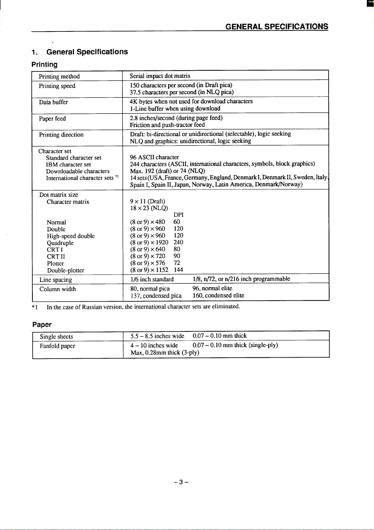
1. General Specifications
Pr
Printingmethod
Piintingspeed
Databuffer
Paperfeed
Printingdirection
Characterset
Standardcharacterset
IBMcharacterset
Downloadablecharacters
Internationalcharactersets”’
Dotmatrixsize
Charactermatrix
Normal
Double
High-speeddouble
Quadruple
CRTI
CRTII
Plotter
Double-plotter
Linespacing
Columnwidth
InthecaseofRussianversion,theinternationalcharactersetsareehmmated.
*1
Serialimpactdotmatrix
150characterspersecond(in Draft pica)
37.5charactersper second(inNLQpica)
4Kbyteswhennotusedfordownloadcharacters
l-Linebufferwhenusingdownload
2.8inches/second(duringpagefeed)
Frictionandpush-tractorfeed
Draft:bi-directionalor unidirrxxional(selectable),logicseeking
NLQandgraphics:unidirectional,logicseeking
96ASCIIcharacter
244characters(ASCII,internationalcharacters,symbols,blockgraphics)
Max.192(draft)or74(NLQ)
14sets(USA,France,Germany,England,DcnmarkI,DenmarkII,Sweden,Italy
SpainI, SpainII,Japan,Norway,LatinAmerica,Denmark/Norway)
9 x 11(Draft)
18X23(NLQ)
DPI
(8or9) x480 60
(8or9) x960 120
(8or9) x960 120
(8or9) x 1920 240
(8or9) x640 80
(8or9)x 720 90
(80r9) x576 7
(8or9) x 1152 144
1/6inchstandard
80,normalpica
137,condensedpica
1/8,nf72,orn/216inchprogrammable
96,normalelite
160,condensedelite
.. . .
P
Singlesheets
Fanfoldpaper
5.5- 8.5incheswide 0.07-0.10 mmthick
4-10 incheswide 0.07-0.10 mmthick(single-ply)
Max,0.28mmthick(3-ply)
-3-
Page 8

GENERAL SPECIFICATIONS
Pr
Dimensions
Weight
Power
Powerconsumption
Environment
Print head
Ribbon
Option
Pain
Interface
Synchronization
Handshaking
Logiclevel
Connector I 57-30360Am~henol
Height120mm(4.7inches)
Depth301mm(11.8inches)
5.1kg (11.2pounds)
120VAC*1O%,60 Hz.
240VAC+1O’%,50/60Hz.
Typ.36W.Max.80W
Operatingtemperature:5 to 40”C(41to I04”F)
Operatinghumidity:10to 80%,noncondensation
Storagetemperature:–30to 65°C(-22 to 149°F)
Storagehumidity:10%to 95%(at40°C)(nocondensation)
9 pins
Life:100milliondots
Fabricribboncartridge
Life:1milliondraftcharacters
Automaticsheetfeeder
Serial-Parallelconverter(SPC-8K)
Centronics-compatible
Byexternalsuppliedstrobepulses
ByACKor BUSYsignals
Width396mm(15.6inches)
220VAC+1O%,50/60Hz.
%
I
I
Fig. 1-1ExternalDimensions
–4-
Page 9
I
“a’enK
GENERAL SPECIFICATIONS
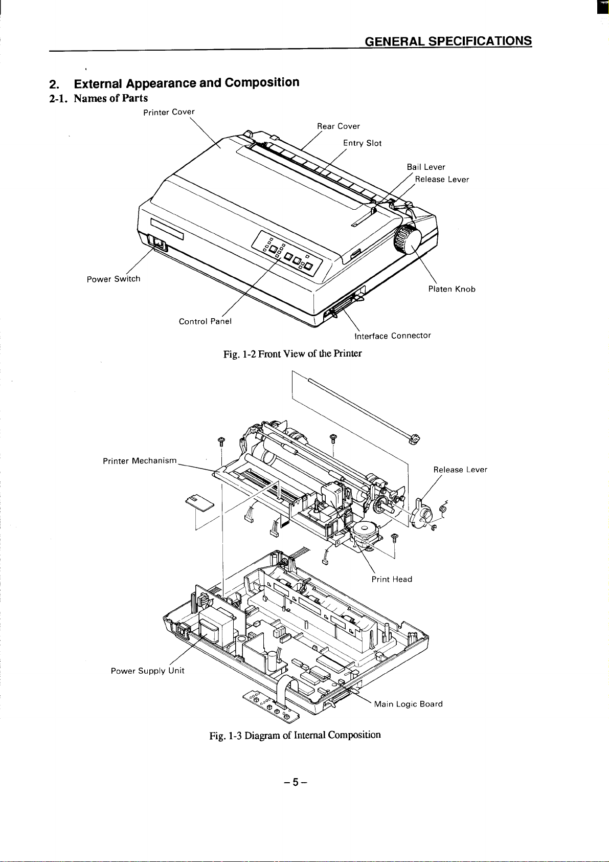
External Appearance and Composition
2.
N P
2
P C
R C
B L
/ L
‘ C
Fig. 1-2FrontViewofthePrinter
P M
-
I C
a L
Fig.1-3DiagramofInternalComposition
-5-
Page 10

GENERAL SPECIFICATIONS
2 S S
\
/
I
1
Fig. 1-4TheDIPSwitchesarelocatedunderthePrinterCover
1) ExceptforRussianversion
Switch
1-1
Function
Printermode
ON OFF
Standard IBM
I 1-2 I Usageof RAM I Buffer
1-3
1-4
1-5
\ 1-6 I Oratorlowercase
1-7
1-8
k
1
AutoLF
No Yes
Autosheetfeeder Inactive
Pawr-outdetector
Enabled Disabled
I Smallcam I Lowercase
Pagelength
1
(See right)
Characterset
2-1
Characterset
(Standardmode) ‘raphics ‘wlics
(IBMmode) ‘et#2
2-2
2-3
Internationalcharacterset(Seeright)
2-4
D S 1
I Download
Active
Set#1
/
D S 2
O
P l
Inc s
Country
U.S.A.
France
Germany
England
DenmarkI*
Sweden
Italy
SpainI
Denmark/Norwaywhenswitc2-1is ON.
*
2 2
ON ON ON
OFF ON ON
ON OFF ON
OFF OFF ON
ON ON
OFF
ON
OFF OFF
ON
OFF OFF
2
OFF
OFF
OFF
2) ForRussianversion
I Switch \
Function
I 1-1 I Printermode
1-2
1-3
I-4
UsageofRAM Buffer Download
AutoLF No Yes
Autosheetfeeder Inactive Active
I 1-5 I Parer-outdetector
14
Character/Command
1-7
PageLength 11inches 12inches
Characterset Set#1 Set#2
Codepage
t---i
1-8
2-1
2-2
2-3
I 2-4 I Notused
ON
I
\ OFF
I Standard I IBM I
I Enabled I Disabled \
(Seeright)
(See right)
I I
-
Ch
I
( s 1 i o
Character/Command
Italiccancel
Italicselect
MSBnotcontrol
MSB=l
1-6
ON
OFF
ON
OFF
1-7
ON
ON
OFF
OFF
C p
Codepage
‘ R 1%---wl
#3840IBM-Russian
Gost
2-2
1
OFF
I OFF / OFF
2-3
I
ON
I
Page 11

2
1)
2)
Atoffline
H
tl
Hold
Push
S p f
S p p
Agingmode
R m
Forwardm
F
w
*1 In thecaseof Russianversion,“ORATOR”fontis eliminated.
–7–
Page 12
G SPECIFICATIONS
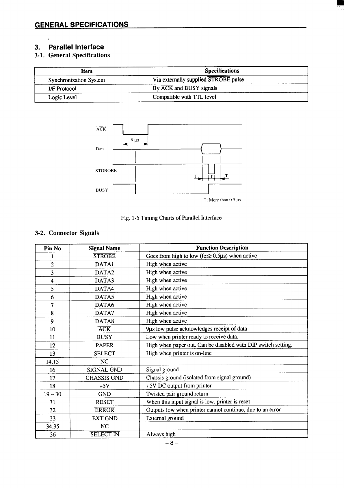
3. Parallel interface
3-1.GeneralSpecifications
Item
SynchronizationSystem
I/FProtocol
I LogicLevel
‘“d ~
STOROBE
Busy
3-2. ConnectorSignals
ACK
ViaexternallysuppliedSTROBEpulse
ByACKandBUSYsignals
I CompatiblewithTTLlevel
9 ~s
h
1
Fig. 1-5TimingChartsofParallelInterface
Specifications
I
T
+
T: More than().5 ILS
PinNo SignalName
1
STROBE
2 DATA1
3
DATA2
4 DATA3
5
6
7
8
9
10
11
DATA4
DATA5
DATA6
DATA7
DATA8
ACK
BUSY Lowwhenprinterreadytoreceivedata.
Goesfromhighto low(for>0.5ps)whenactive
Highwhenactive
Highwhenactive
Highwhenactive
Highwhenactive
Highwhenactive
Highwhenactive
Highwhenactive
Highwhenactive
9VSlowpulseacknowledgesreceiptof data
FunctionDescription
12 PAPER Highwhenpaperout.Canbe disabledwithDIPswitchsetting.
13
SELECT
Highwhenprinterison-line
14,15 NC
16
17
18
SIGNALGND
CHASSISGND
+5V +5VDCoutputfromprinter
19-30 GND
31
32
33
34,35
RESET Whenthisinput signalis low,printerisreset
ERROR
EXTGND Externalground
NC
36 SELECTIN
Signalground
Chassisground(isolatedfromsignalground)
Twistedpairgroundreturn
Outputs lowwhenprintercannotcontinue,duetoan error
Alwayshigh
-8–
Page 13
GENERAL SPECIFICATIONS
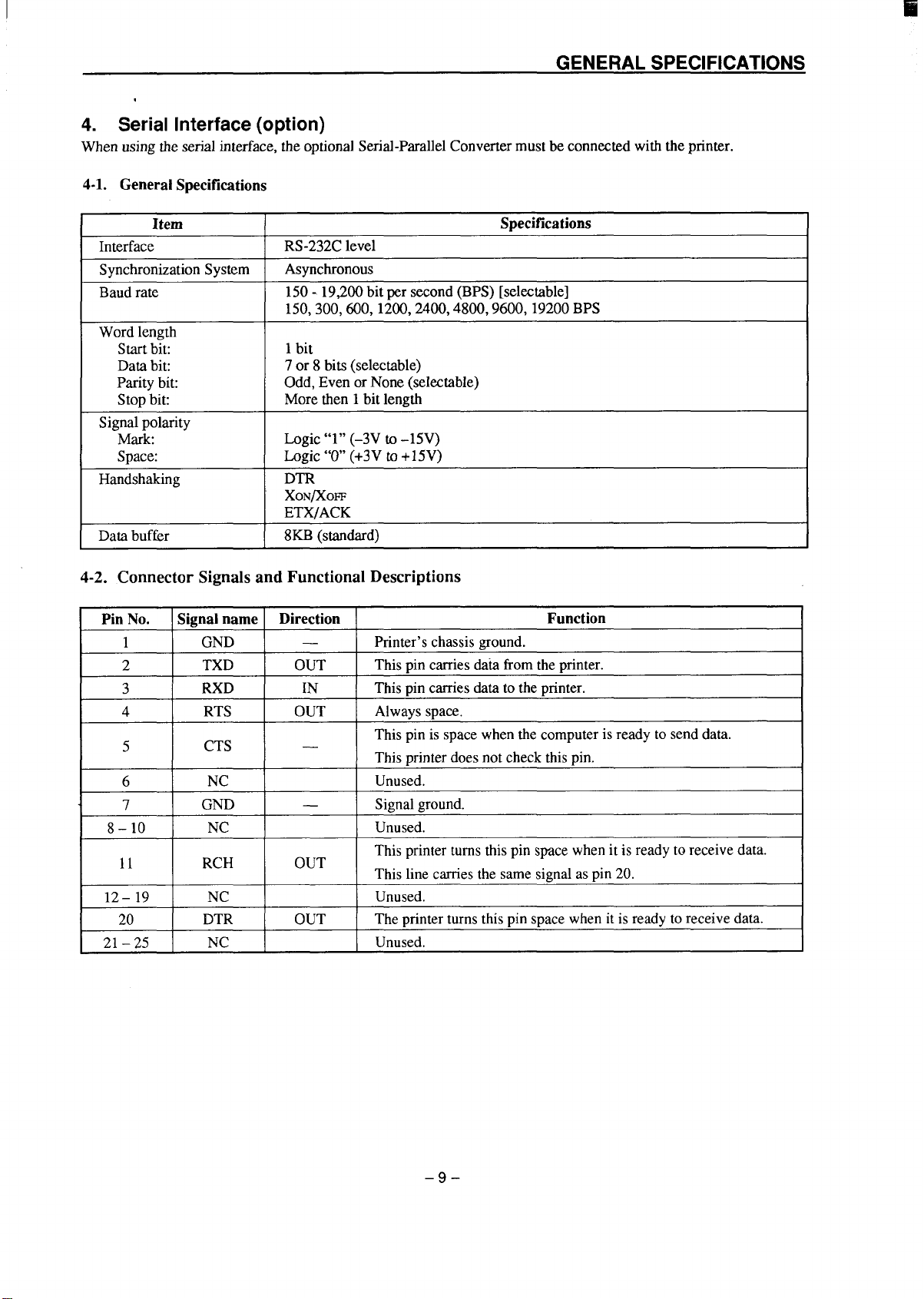
Serial Interface (option)
Whenusing theserialinterface,theoptionalSerial-PmallelConvertermustbeconnectedwiththeprinter.
4-1. GeSpe
Item
Interface
SynchronizationSystem
Baudrate
Wordlength
Startbit:
Databit: 7or8 bits(selectable)
Paritybit: Odd,EvenorNone(selectable)
Stopbit:
Signalpolarity
Mark:
Space:
Handshaking
Databuffer 8KB(standard)
4-2. Connector Signals and Functional Descriptions
Pin No. \Signal name I Direction
I
1 GND
2
3
4
5
6
7
8-10
11
12– 19
20
21–25 NC
TXD OUT
RXD IN
RTS OUT Alwaysspace.
CTS
NC
GND
NC
RCH OUT
NC
DTR OUT
RS-232Clevel
Asynchronous
150-19,200 bitpersecond(BPS)[selectable]
150,300,600>1200,2400,4800,9600, 19200BPS
1bit
Morethen1bit length
Logic“l” (-3V to-15V)
Logic“O”(+3Vto+15V)
DTR
XON/xOFF
ETX/ACK
—
.
—
Printer’schassisground.
Thispincarriesdaiafromtheprinter.
Thispincarriesdatato theprinter.
Thispinis spacewhenthecomputerisreadyto senddata.
Thisprinterdoesnotcheckthispin.
Unused.
Signalground.
Unused.
Thisprinterturnsthis pin spacewhenit is readymreceivedata.
Thislinecarriesthesamesignalaspin20.
Unused.
Theprinterturnsthispinspacewhenitisreadyto receivedata.
Unused.
Specifications
Function
–9–
Page 14

GENERAL SPECIFICATIONS
4-3. DIP Switch Settings
Switch
I
1 8data bits
2
3
4
5
6
7
8
AllswitchedaresetON whentheprinterleavesthe factory.
I
I
Baud rate Switch 6
150
Noparity
Handshakingprotocols- seetablebelow
Oddparity
Datatransferrate– seetablebelow
Protocol
DTRmode
XON/XOFFmode
ETX/ACKmode
300
600
I
I
1200
2400
4800
9600
19200
ON
7 databits
Paritychecked
Evenparity
Switch
I
I
Switch 7
OFF
OFF
OFF
OFF
\
ON
ON
ON
ON
I
I
I
3
ON
ON
OFF
OFF
OFF
ON
ON
OFF
OFF
ON
ON
OFF
I
I
I
I
Switch 4
ON
OFF
ON
Switch 8
OFF
ON
OFF
ON
OFF
ON
OFF
ON
I
I
I
I
I
1
I
–10 –
Page 15
C 2
T O
1. B Di
M L B
2
2 GeF C
D I Op
2 PaIn
2 S In
2 Ed........................................................................................9
2 P H D C
2 P H TeDeC
2 CaM D C
2-2-5. CaM S C
2-2-6.P F M D C
.....................................................................................................
................................................................................................
.............................................................................................
................................................................................................
...................................................................................................
...............................................................................................
.................................................................................
......................................................
.........................................................................
.........................................................................
....................................................................
1
1
1
1
1
1
1
1
20
2
2
l
2
2
2
P S U
3
4 Me
4-1.
4
4
4
4
R Ci
R b + L V De
PrCi
P H Me
P H CaMe
I R F Me
P F Me
De
..........................................................................................................
..................................................................
..................................................................................................
..............................................................................................
.........................................................................................................
..........................................................................................
..........................................................................
................................................................................
........................................................................................
................................................................................................................
2
2
2
2
2
2
2
2
2
30
Page 16

I
Page 17
I
THEORY OF OPERATION
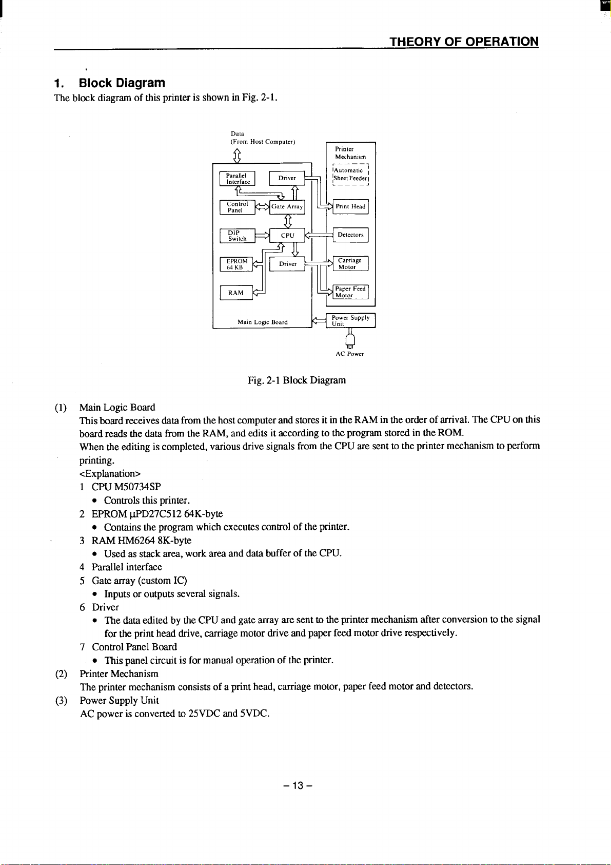
Block Diagram
1.
Theblockdiagramofthisprinteris shown in Fig.2-1.
DaLa
(From Host Comp.tcr)
8
Parallel
Interface
Driver
Printer
Mechamsm
~-———.
IAutomat,c ~
~SheetFeederl
.——— —.
Control
[
EPROM
64 KB
I
+};
Panel
~ju~
DIP
Switch
RAM
Main Logic Board
Gate Array
Driver
7 .~
Print Head
Detectors
!’
Carriage
4
Paper Feed
Motor
Power
Unit
AC Power
Motor
1
s
(
Fig.2-1BlockDiagram
(1) MainLogicBoard
Thisboardreceivesdatafromthehostcomputerandstoresit intheRAMinthe orderofarrival.TheCPUon this
boardreadsthedatafromtheRAM,andeditsitaccordingto theprogramstoredin theROM.
Whentheeditingiscompleted,variousdrivesignalsfromtheCPUare sent to theprintermechanismto perform
printing.
<Explanation>
1
CPUM50734SP
● Controlsthis printer.
2
EPROMP.PD27C51264K-byte
. Containstheprogramwhichexecutescontroloftheprinter.
RAMHM62648K-byte
3
● Usedasstackarea,workareaand databufferof theCPU.
4
Parallelinterface
5
Gatearray(customIC)
. Inputsoroutputsseveralsignals.
Driver
6
● ThedataeditedbytheCPUandgatearrayare sent to theprintermechanismafterconversionto the signal
fortheprintheaddrive,carriagemotordriveandpaperfeedmotordriverespectively.
7
ControlPanelBoard
. Thispanelcircuitis formanualoperationoftheprinter.
(2) PrinterMechanism
Theprintermechanismconsistsofa printhead,carriagemotor,paperfeedmotoranddetectors.
(3) PowerSupplyUnit
ACpowerisconvertedto25VDCand 5VDC.
– 13–
Page 18
THEORY OF OPERATION
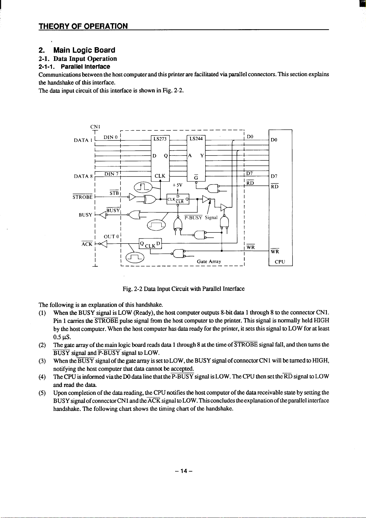
2. Main Logic Board
I O
2-1-1. PaIn
Communicationsbetweenthehostcomputerandthisprinterarefacilitatedviaparallelconnectors.Thissectionexplains
thehandshakeof thisinterface.
Thedatainputcircuit of thisinterfaceisshowninFig.
2-2.
CNI
1-
DATA1I
I
I
DATA8
STROBE
BUSY
I
I
ACK
~ ————————————————————,
DIN O]
DIN 7 \
—1
STBI
(
1
I
I
I
I
@
LS273
DQ
CLK
A
I
I
I
L ————————— — — — — —— ———
Q
LS244
AY
ii
5V
+
GateArray
————
; DO
r
1
I
r
I
1
I
[
i D7
!= ~
I
I
I
I
I
I
I
l—
IWR
I
I
I L
DO
- D7
Iii
CPU
Fig.2-2DataInputCircuitwithParallelInterface
Thefollowingisan explanationofthis handshake.
(1)
WhentheBUSYsignalis LOW(Ready),thehost
computer outputs 8-bitdata 1through8 totheconnectorCN1.
Pin 1carriestheS&OBE pulsesignd-hm thehost~mputer &theprinter.ThissignalisnormalIyheld HIGH
bythe hostcomputer.Whenthehostcomputerhasdatareadyfortheprinter,itsetsthissignaltoLOWforatleast
0.5p.s.
(2)
gatearrayofthemainlogicboardreadsdata1through8atthetimeofSTROBEsignalfall,andthenturnsthe
The
BUSYsignalandP-BUSYsignaltoLOW.
Whenthe BUSYsignalofthegatearrayissettoLOW,theBUSYsignalofconnectorCNlwillbeturnedtoHIGH,
(3)
notifyingthehost computerthatdatacannotbe accepted.
(4)
TheCPUisinformedviatheDOdatalinethattheP-BUSYsignalisLOW.TheCPUthensettheRDsignaltoLOW
andread thedata.
(5)
Uponcompletionofthedatareading,theCPUnotifiesthehostcomputerofthedatareceivablestatebysettingthe
BUSYsignalofconrtectorCNIandtheACKsignaltoLOW.Thisconcludestheexpkmationoftheparallelinterface
handshake.Thefollowingchartshowsthetimingchartof thehandshake.
–14 –
Page 19
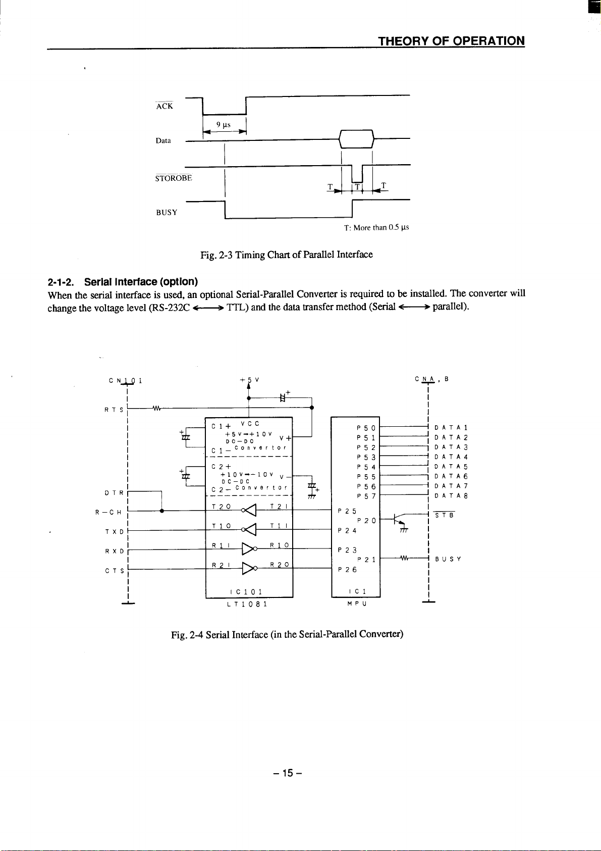
““K u
D
w
THEORY OF OPERATION
9
)
I
STOROBE
- i
BUSY
2-Ser(o
Whentheserialinterfaceis used,an optionalSerial-ParallelConverterisrequired to be installed.The converterwill
changethevoltagelevel(RS-232C
C 1
I
R
T
,
1
~ TTL)andthedatatransfermethod(Serial
I
Fig.2-3TimingChartof ParallelInterface
R
I 4
T
I
T
TT
J-Ill
I
M t (
~ parallel).
C B
P50
P
P
P
P
P
P
P
T=
P
P
P
P
P
P
, D
,
, D
1
I
I
I
D
D
D
D
D
S
B
I
$-
1
Fig.2-4SerialInterface(intheSeriai-ParaiielConverter)
– 15-
M
I
Page 20
THEORY OF OPERATION
TheIC101isadualRS-232Cdriver/receiverwhichincludesa capacitivevoltagegeneratorto supplyRS-232Cvoltage
levelsfroma single5Vsupply.
DatafromthehostcomputerissentfromRXDviaICIOlandisinputtotheMPU.SerialdatainputtotheMPUisconverted
intoparalleldata,andoutputtothemainlogicboard.Conversely,paralleldatareceivedbytheMPUisconvertedthere
intoserialdata,andoutputtothe TXDterminalviaIC101.
TheCTSterminalishardware-connected,notsoftware-connected.(Thissignalisnotchecked.)
Thisprinter employs 3 differenttransfermethods,whichcanbe selectedusingthedip switches.(Referto Chapter1,
4-3
SettingDipSwitches)
(1)
DTRmethod
TheDTRsignalisconsideredaBUSYsignalatthehandshake,andwhenthedata buffercapacityis256bytesor
less,theDTRsignalis givena markedstatus,meaningitcannotreceivedata.Whenthecapacityofthedatabuffer
increasesto512bytes or moreduringprinting,theDTRsignalis givena spacestatus,whichindicatesthatit can
receivedata.
(2)
XoN/Xommethod
Whena handshakeiscarriedoutwiththehost computer,theXoN/Xommethodmakesuseof ASCIIcodes(DCl
andDC3).(DClandDC3arecalledXONandXom,respectively.)Whentheprinterbufferisfull,DC3(ASCIIcode
19)is outputtotheTXDterminal,andthecomputerreceivesarequesttostopdatatransfer.ThepnnteroutputsDC3
untilit(thecomputer)stopsdatatransfer.Duringprinting,whenthebufferfullstatusiscancelledanddatacanbe
received,DC1(ASCIIcode17)isoutputtotheTXDterminal.WhenDC1isoutputfromtheprinter,thecomputer
followsthedataformat,andbeginsdatatransfer.DatatransferwillcontinueuntilDC3 isoutputagain.
(3)
ETX/ACKmethod
Thedatablockisconfiguredasshownbelow,buttheinitialSTXcodeisnotnecessary.WhenanSTXcodeissent
fromthehostcomputer,that1byteisignored.Whenthe ETXcodeisreceived,that1byteisnotregardedasdata,
anACKorNACKcodeis senttotheTXDterminal,andthehostcomputerisinformedthatdatareceptionhasbeen
completed.
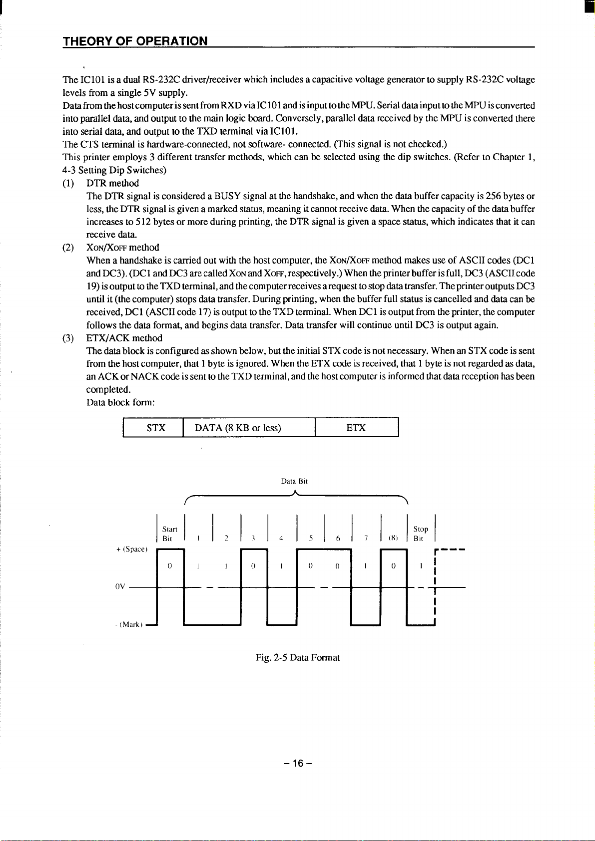
Datablockform:
+(
—
ETX
6 7
0
(
1
0
1
stop
B
---
,;
–-+
I
I
STX
S
B
—
(
DATA(8KBorless)
I ? 3 4
—
Fig. 2-5DataFormat
D B
5
1
–16 –
Page 21
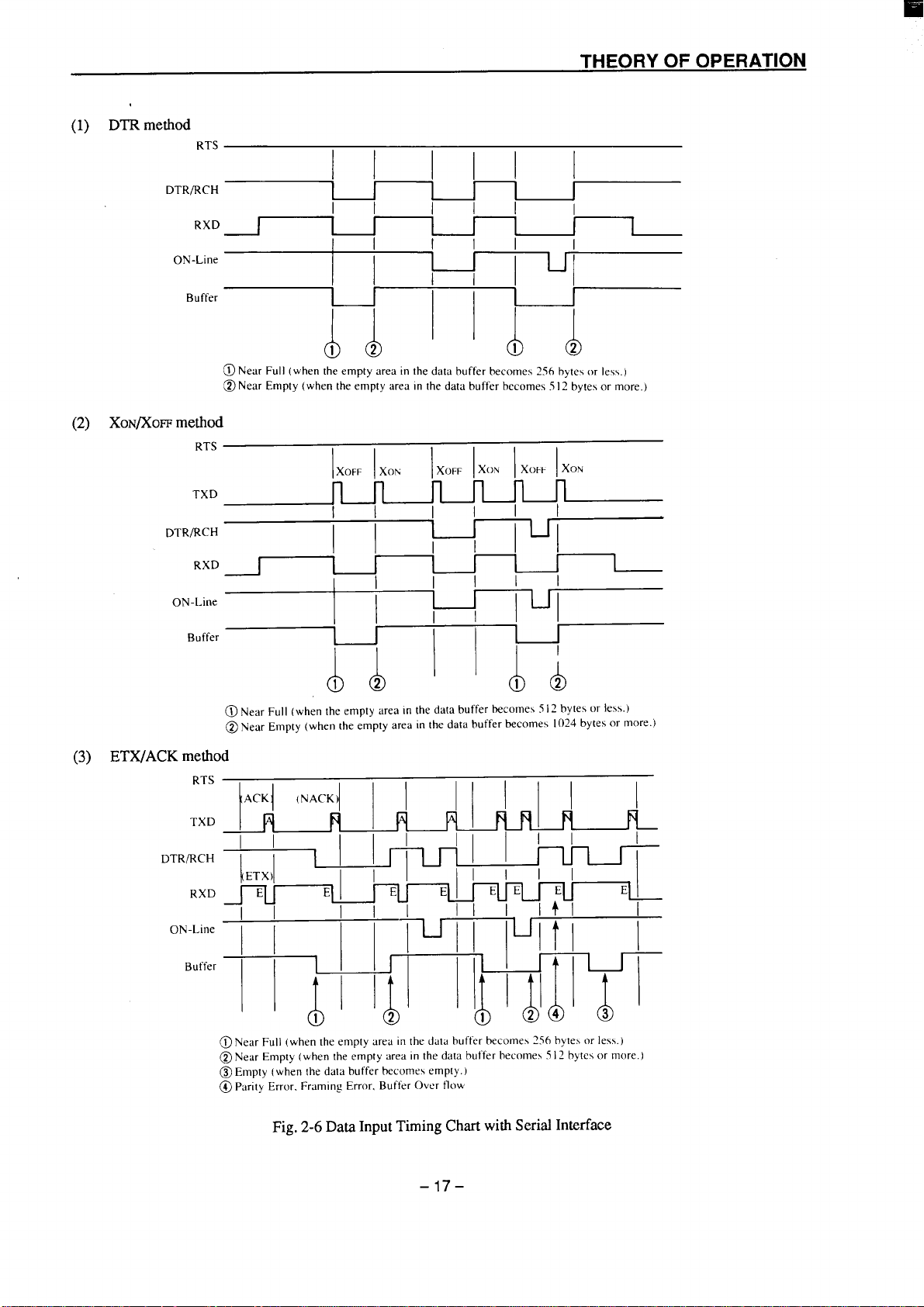
(1) DTRmethod
THEORY OF OPERATION
R
‘T~
“
O
(2) XoN/xoFFmethod
R
T
D
R
O
I I
I
I
I I
Ill
I
,
1
I 2
All
X();t ‘
1
1
12
u
@
N F (w t e a t d b b 2 h l )
@ N E ( t e a t d b b b m
X
X
1
1
II
X x
1
1111
II
1
I
B
(3) ETX/ACKmethod
R
T
D
R
O
B
@ N F (w t e a t d b b 2 h l )
@ N E ( [ e a t d b b b m
@ E ( t d b b e )
@ P E F E B O f
@ N F ( t e f t d b b b l
@ N E ( [ e a t d b b 1 b m
A (
I
II
v
II
E
E
1
F
F
II
E
E E
I I I II I
1111
F N
F
II
‘1tI
I
I I 11 I
F–
E
Fig. 2-6DataInputTimingChartwithSerial Interface
– 17–
Page 22
THEORY OF OPERATION
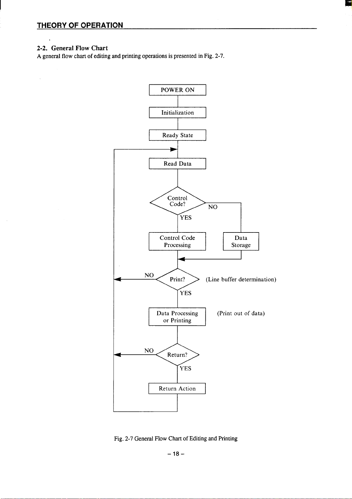
2 General Flow C
Ageneralflowchartofeditingand printingoperationsispresentedinFig.2-7.
POWER ON
I
1
&
Read Data
T
NO
YES
Control Code
Processing Storage
4
Data
t (L
Data Processing
or Printing
(Print out of data)
Q
4
Fig.2-7GeneralFlow ChartofEditingandPrinting
NO
Return Action
–18 –
Page 23
THEORY OF OPERATION
2-2-1. Editing
Datastoredin theRAMisreadoutsequentiallyby theCPUandtheneditedaccordingtoa functioncodethathasbeen
specifiedinadvance.
ThiseditingtakesplacesuntiltheCRorCR+ LF codeappearsorthe linebufferbecomesfull.
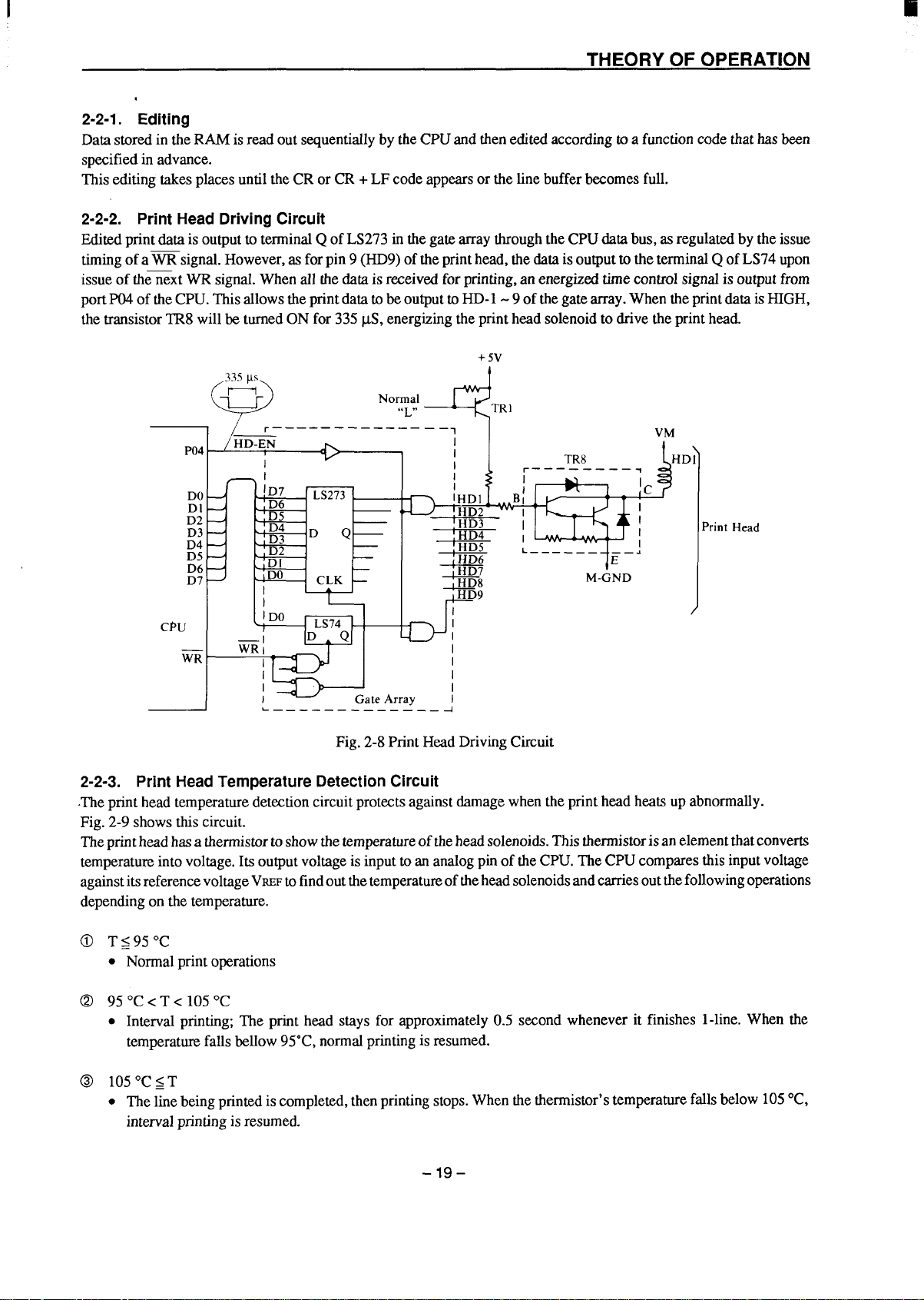
2-2-2. P H DrCi
EditedprintdataisoutputtoterminalQof LS273inthegatearraythroughtheCPUdatabus,asregulatedbytheissue
timingofa WRsignal.However,as forpin9 (HD9)oftheprinthead,thedataisoutputtotheterminalQofLS74upon
issue of thenextWRsignaI.Whenallthe datais receivedforprinting,anenergizedtimecontrolsignalis outputfrom
portP04oftheCPU.ThisallowstheprintdatatobeoutputtoHD-1-9 ofthegatearray.WhentheprintdataisHIGH,
thetransistorTR8willbe turnedONfor 335pS, energizingtheprintheadsolenoidto drivetheprint head.
+ 5V
\
D1
p H
/
Fig.2-8Print HeadDrivingCircuit
2-2-3. P H TeDeC
.Theprintheadtemperaturedetectioncircuitprotectsagainstdamagewhentheprint headheatsup abnormally.
Fig.2-9 shows thiscircuit.
Theprintheadhasa thermistortoshowthetemperatureoftheheadsolenoids.Thisthermistors anelementthatconverts
temperatureintovoltage.Itsoutputvoltageisinputto an analogpinof theCPU.TheCPUcomparesthisinputvoltage
againstitsreferencevoltageVwFtofindoutthetemperatureoftheheadsolenoidsandcarriesoutthefollowingoperations
dependingonthetemperature.
0 Ts95“C
● Normalprint operations
@ 95“C c T < 105‘C
. Intervalprinting;The print head stays for approximately0.5 secondwheneverit finishesl-line. When the
temperaturefallsbellow95”C,normalprintingisresumed.
@ 105‘C ST
. Thelinebeingprintediscompleted,thenprintingstops.Whenthethermistor’stemperaturefallsbelow105“C,
intervalprintingisresumed.
- 19–
Page 24
+5V
T
Y $
F ( ~
I
Fig.2-9Print HeadTemperatureDetectionCircuit
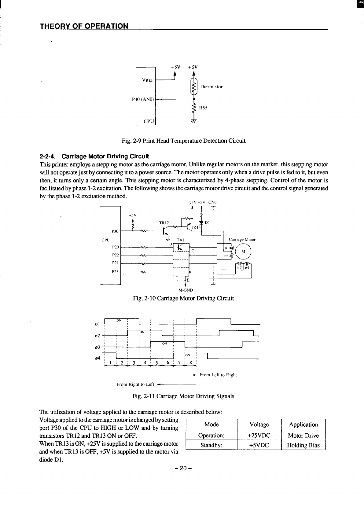
2-2-4. CaM DrC
This printeremploysasteppingmotorasthecarriagemotor.Unlikeregularmotorsonthemarket,this steppingmotor
willnotoperatejustby connectingittoa powersource.Themotoroperatesonlywhena drivepulseisfedtoit,buteven
then,it turnsonlya certainangle.This steppingmotoris characterizedby 4-phasestepping.Controlof the motoris
facilitatedbyphase1-2excitation.Thefollowingshowsthecarriagemotordrivecircuitandthecontrolsignalgenerated
bythephase
1-2
excitationmethod.
+ + C
1 *
C
p
P
P
P
Fig.2-10CarriageMotorDrivingCircuit
1
;
(
–20
I
;
F L R
Mode
Operation: +25VDC
Standby:
–
01 :
03 ; :
Theutilizationof voltageappliedtothecarriagemotorisdescribedbelow:
Voltageappliedtothecarriagemotorischangedbysetting
portP30 of the CPU to HIGH or LOW and by turning
transistorsTR12andTR13ONorOFF.
WhenTR13isON,+25Vissuppliedtothecarriagemotor
andwhenTR13isOFF,+5Vis suppliedtothemotorvia
diodeD1.
;ON :
; , I : I
,,; ,
F R L ~
L
Fig.2-11CarriageMotorDrivingSignals
Carriage MOICN
Voltage Application
MotorDrive
+5VDC HoldingBias
Page 25
I
THEORY OF OPERATION
2-2-5. Carriage M S C
Sincethecarriagemotoris a steppingmotor,tie carriagecanbestoppedatadesiredpositionbycontrollingacceleration
anddeceleration.Thecarriagecanalsomovebackward.
Therotationalspeedof thecarriagemotoris setby thenumberof pulsespertimeunit.Thecharacterpitch(horizontal
chamctersize)in eachprintmodeisdeterminedby changingthisrotationalspeed(orcarriagetransferspeed).
(1) Atstart-upof themotor:
Thenumberofpulsesinput to themotorincreasein steps,reachinga certainfrequency.
(2) Tostop themotoc
Thenumberof pulsesinputtothemotordecreasesinsteps,in orderto graduallybringthemotortoa halt.
(3) Whenprintingiscarriedout:
Pulsesof a uniformpulsewidthare suppliedforprinting.
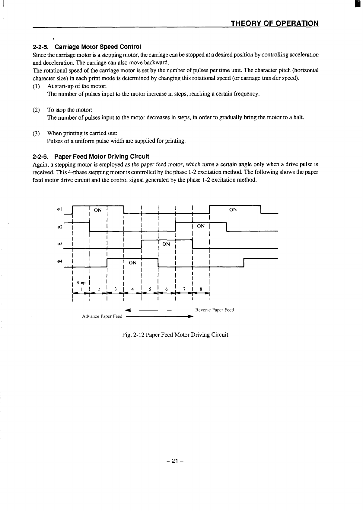
2-2-6. P F M DrC
Again,a steppingmotoris employedasthepaperfeed motor,whichturnsa certainangleonlywhena drivepulseis
received.This4-phasesteppingmotoriscontrolledby the phase1-2excitationmethod.Thefollowingshowsthepaper
feedmotor drivecircuitand thecontrolsignalgeneratedbythephase1-2excitationmethod.
Fig.2-12PaperFeedMotorDrivingCircuit
-21 –
Page 26
6
+
T
P
T
P
P
T
P
T
P
)
)
t
C
I
I
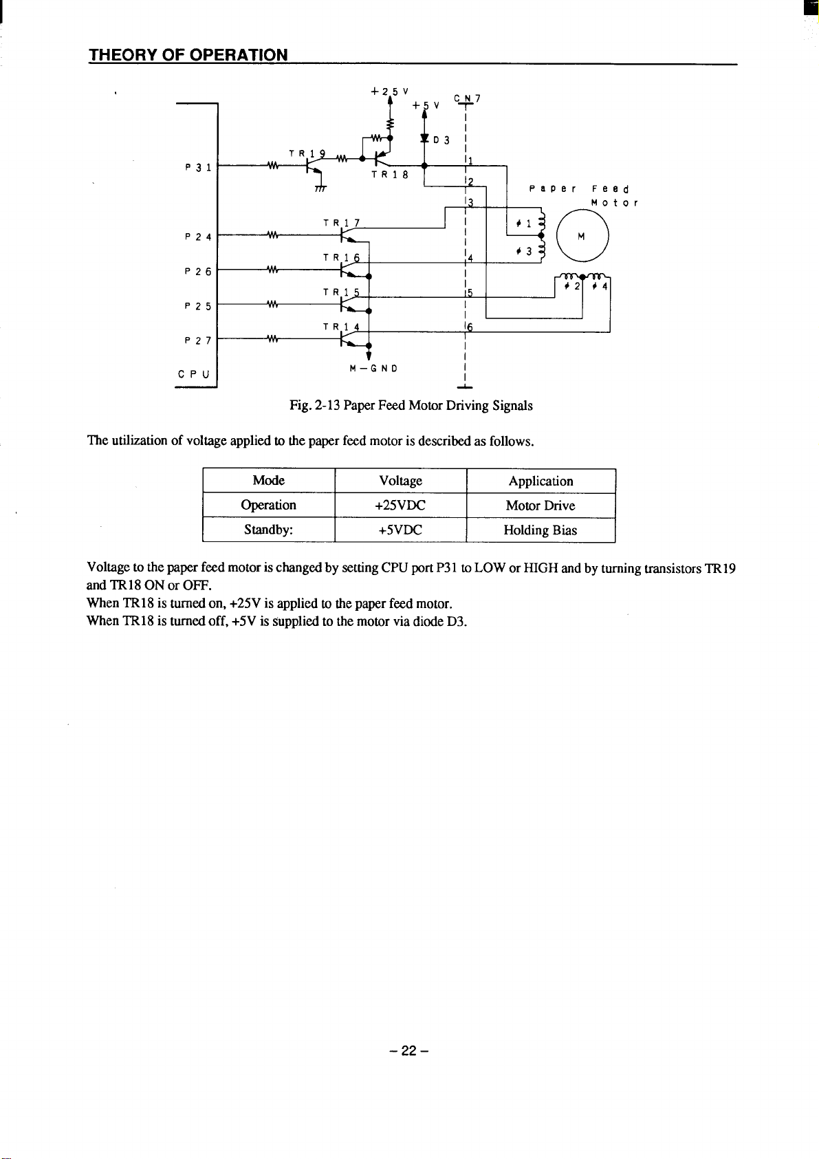
Fig.2-13PaperFeedMotorDrivingSignals
Theutilizationof voltageappliedto thepaper feedmotorisdescribedasfollows.
Mode Voltage Application
1
LD3 I
C
I
I I
13
+3
-+0
4
I
I
I
I
&
P F
M
d
Mot
Operation
Standby:
VoltagetothepaperfeedmotorischangedbysettingCPUportP31toLOWor HIGHandbyturningtransistorsTR19
andTR18ONorOFF.
WhenTR18isturnedon,+25Visappliedtothepaperfeedmotor.
WhenTR18isturnedoff,+5Vis suppliedtothemotorviadiodeD3.
+25VDC
+5VDC HoldingBias
MotorDrive
- 22–
Page 27
1
THEORY OF OPERATION
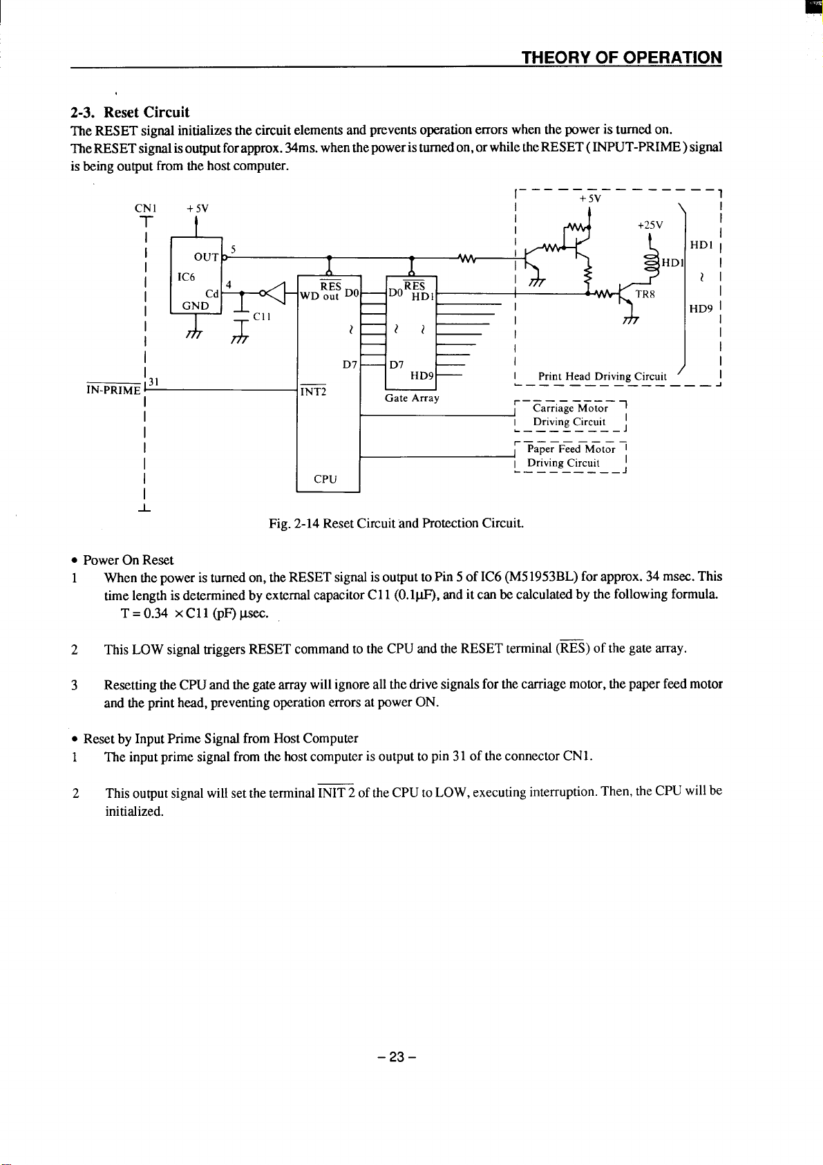
2 R Ci
T RESETsignalinitializesthecircuitelementsandpreventsoperationerrorswhenthepoweristurned on.
TheRESETsignalisoutputforapprox.34ms.whenthepoweristumedon,orwhiletheRESET(INPUT-PRIME)signal
is beingoutputfromthehostcomputer.
——
\
HDI
HD
(
HD9
IN-PRIME
CN1
T
I
I
/
I
+ .5V
t
OUT D
IC6 ~
GND
.———————— — ———
I
I
I
5
1
,
c1 1
J=
WD%? Do —
)
r I
1
DOR&
))
I
I
I
d
+ 5V
A
+25V
I
Fig.2-14ResetCircuitandProtectionCircuit.
● PowerOnReset
1 Whenthepoweristurnedon,theRESETsignalisoutputtoPin5 ofIC6(M51953BL)forapprox.34msec.This
timelengthisdeterminedbyexternalcapacitorCl 1(0.lP.F),anditcanbe calculatedbythe followingformula.
T = 0.34
2 ThisLOWsignaltriggersRESETcommandto theCPUandtheRESETterminal(RES)of thegatearray.
Resettingthe CPUandthegatearraywillignoreallthedrivesignalsforthe carriagemotor,thepaper feedmotor
3
andthe printhead,preventingoperationerrorsatpowerON.
. Resetby InputPrimeSignalfromHostComputer
1 Theinputprimesignalfromthehostcomputerisoutputtopin 31of theconnectorCN1.
2 ThisoutputsignalwillsettheterminalINIT2 oftheCPUtoLOW,executinginterruption.Then,theCPUwillbe
initialized.
X Cll (PF)WK.
–23 –
Page 28
THEORY OF OPERATION
2 R b + V D
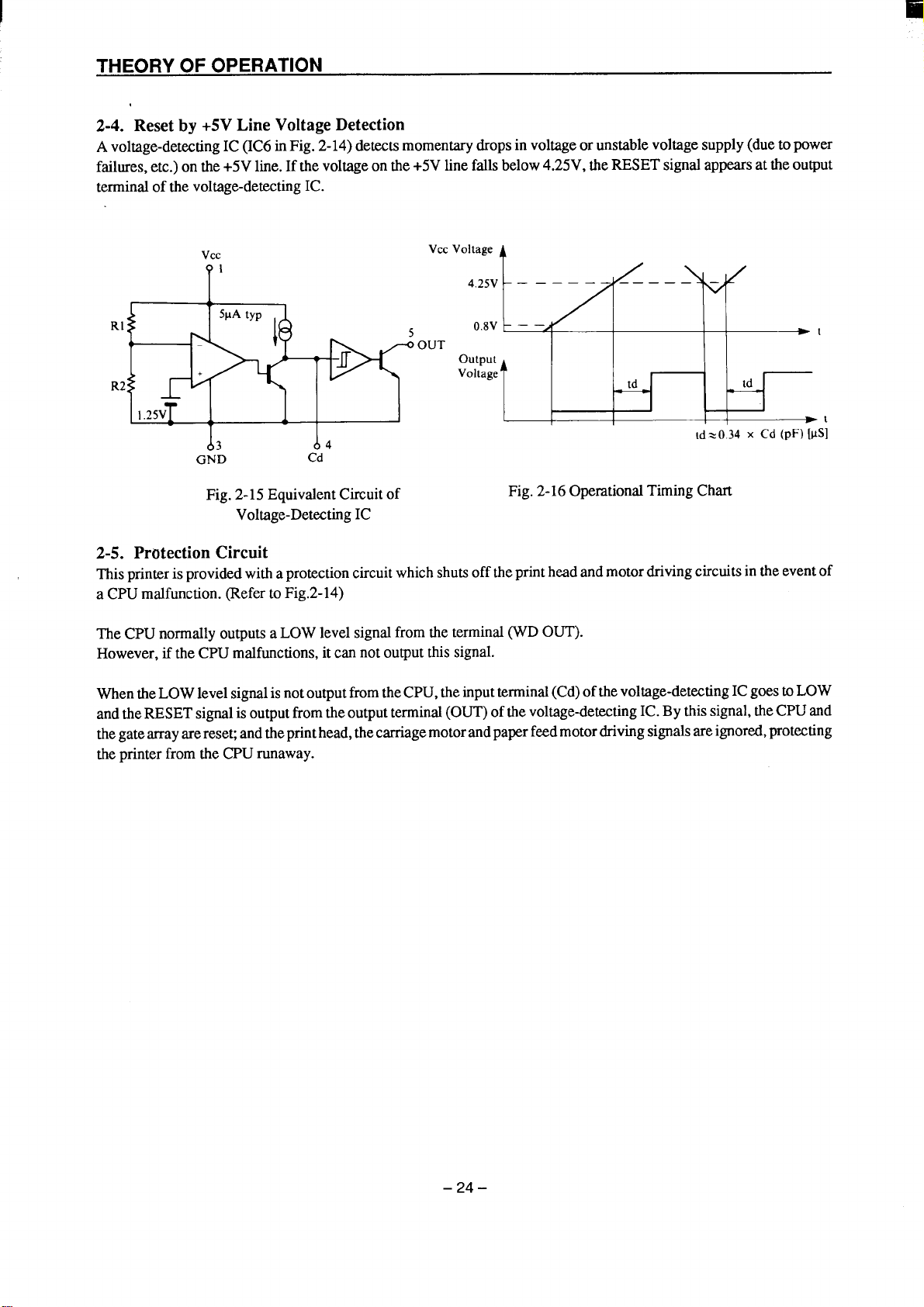
Avoltage-detectingIC(IC6inFig.2-14)detectsmomentarydropsin voltageorunstablevoltagesupply(duetopower
failures,etc.)on the+5Vline.Ifthevoltageonthe+5Vlinefallsbelow4.25V,theRESETsignalappearsattheoutput
terminalofthe voltage-detectingIC.
V
5
OUT
VoltageA
o
V A
–— – ——
~
=
*
X ( [
t
w
R2::
()
1,~sv
V
91
t
5pA
+
1
. .
A4
GND
Cd
Fig.2-15EquivalentCircuitof
Fig.2-16OperationalTimingChart
Voltage-DetectingIC
2
PrWection Circuit
Thisprinterisprovidedwitha protectioncircuitwhichshutsofftheprintheadandmotordrivingcircuitsin theeventof
a CPUmalfunction.(RefertoFig.2-14)
TheCPUnormallyoutputsaLOWlevelsignalfromtheterminal(JVDOUT).
However,iftheCPUmalfunctions,itcan notoutputthissignal.
Whenthe LOWlevelsigmlisnotoutputfromtheCPU,theinputterminal(Cd)ofthevoltage-detectingICgoestoLOW
andtheRESETsigmlisoutputfromtheoutputterminal(OUT)of the voltage-detectingIC.Bythissignal,theCPUand
thegatemay arereset;andtheprirtthead,thecarriagemotorandpaperfeedmotordrivingsignalsareignored,protecting
theprinter fromthe CPUrunaway.
–24 -
Page 29
THEORY OF OPERATION
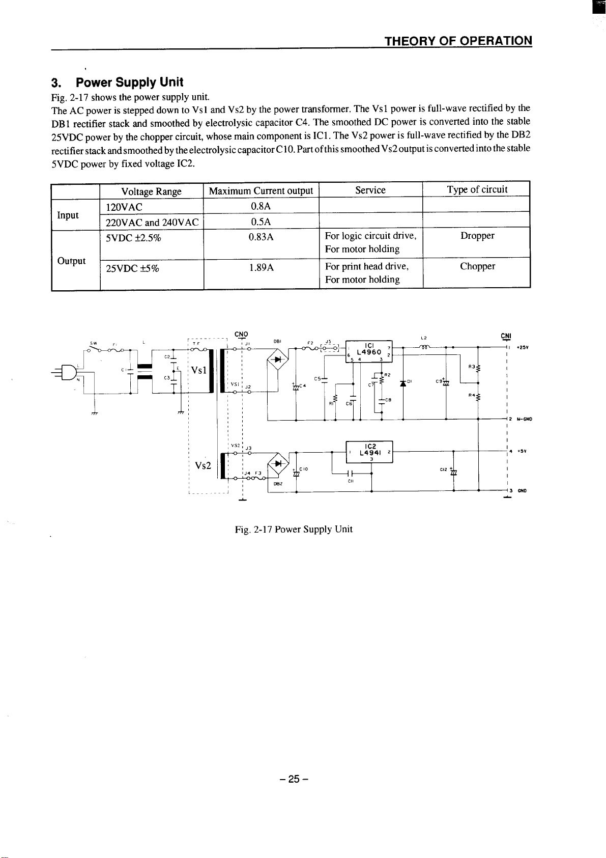
3. Power Supply Unit
Fig.2-17showsthepowersupplyunit.
TheACpowerissteppeddownto Vsl andVS2bythepowertransformer.TheVsl powerisfull-waverectifiedbythe
DB1rectifierstackandsmoothedby electrolysiscapacitorC4. The smoothedDCpoweris convertedintothe stable
25V’DCpowerbythechoppercircuit,whosemaincomponentisIC1.TheVS2 powerisfull-waverectifiedbytheDB2
rectifierstackandsmoothedbytheelectrolysiscapacitorClO.PartofthissmoothedVs20utputisconvertedintothestable
5VDCpowerbyfixedvoltageIC2.
Input
output
VoltageRange
120VAC
220VACand240VAC
MaximumCurrentoutput
0.8A
0.5A
5VDC?2.5% 0.83A
25VDCti%
1.89A
Service
Forlogic circuitdrive,
Formotor holding
Forprintheaddrive,
Formotor holding
Typeofcircuit
Dropper
Chopper
+25V
t
+5V
Fig.2-17PowerSupplyUnit
–25 –
Page 30

THEORY OF OPERATION
WewillexplainthechoppercircuitintermsofFig.2-18,a simplifiedversionofFig.2-17.IC1isa pulse-widthcontrol
switchingregulator.It hasa referencevoltagesection,oscillationsection,pulse-widthcontrol section,and power
transistors.Fig.2-19showsanequivalentcircuitforIC1.
ThechoppercircuitswitchesthepowertransistorsinIC1onandofftodivideinputvoltage
thosepulseswithchokecoilL2andcapacitorC9toobtainthedesiredoutputvoltage
Since thepulse width control sectiondetermines theratio of thetimethatthepower transistorsareonandoff bycomp~ing
the output voltage with the reference voltage, the output
voltagecanbeheldsteady.
Inorderwords,iftheoutputvoltagefallsbelowthereferencevoltage,thepulsewidthcontrollerextendsthetimethatthe
powertransistorsare on,thusraisingtheoutputvoltage.TheoutputvoltageVOUTcanbeexpressedwiththefollowing
equation.
VINintopulsesandsmoothes
VOUT.
Vour = VIN.
TON :
TOFF :
T:
Durationthepowertransistorsareon
Durationthepowertransistorsareoff
TON+ TOFF(constant)
TON
TON+ TOFF
= VIN. +
DiodeD1formsa pathwaythroughwhichtheenergyaccumulatedonchokecoilL2whilethepowertransistor
dischargedwhilethepowertransistorsareoff.
—————————._——————
I
PowerTransistor
o
V
o
I
I
I
I
I
I
I
i
i
I
I
Ic 1
PulseGenerator
Block
I
————
I
1
1—
I
I
I
1 L
LZ
Y
D1
R3
+
4)
z C9
o
o
L _ –
Fig. 2-18ChopperCircuit
a on
is
r-=w-
Os
F C
1
3
(
Inh
\
;w’M
s
‘
I
F
F
R Q--
Q-
1 r
Iv
D
G
i
4
1
Fig. 2-19 Equivalent Circuit for Voltage Regulator IC1
–
–26
Page 31

I
THEORY OF OPERATION
4. Mechanism
P M
Theprintheadconsistsof9 needlewiresand9 printsolenoids.Thefollowingexplainshoweachneedlewireoperates
duringprinting.
(1) Whentheprintsolenoidisenergized,theclapperisattractedbytheironcoreand theneedlewireisdriventoward
theplaten.
(2) Thisneedlewirehitstheplatenviatheinkribbonandpaper.Asingledotisprintedon thepaper.
(3) Whentheprintsdenoidisale-energized,theneedlewireisreturnedtoitsoriginalpositionbyreboundenergyand
springandclapperholder(leafspring)force.
P G
P
I I
S S
N W
I I
.
C H
C
1
4-2.
P C M
print headcarryingmechanismconsistsmainlyofa carriage,timingbelt,carriagemotor,andhomepositiondetec-
tor.
(1)
Carriage
Thecarriageissupportedhorizontallyby meansofthecarriagestayandrearangle,anditmovesfromsidetoside
withtheprintheadmountedaboveit.Atimingbeltis clampedtothebaseof thecarriageanda plateis mounted
atthebaseforhomepositiondetection.
(2)
TimingBelt
Thetimingbeltissuspendedbetweenthetimingpulleyofthecarriagemotorandthetimingpulleyofthetension
lever,and it maintainsaconstanttension.
Thetimingbelt is alsoclampedtothebaseofthecarriagesothatitcanmovethecarriageaccuratelywithdriving
forcefromthecarriagemotor.
(3)
CarriageMotor
Thecarriagemotorisa HB (Hybrid)type,four-phaseand192-polepulsemotor,whichisdrivenbypulsesignals
fromthecontrolcircuit.Therotationalratedependsonthenumberofpulsesperunittime.Byvaryingthisrotational
rate(thatis,thecarriagecarryingrate),the sizeof the horizontalletterscanbe changedineachprint mode.
D
1
o
P I
Fig,2-20OutlineofPrintHeadMechanism
I R
G
I C
B
–27 –
Page 32

I
THEORY OF OPERATION
T B
C M
Fig.2-21PrintHeadCarryingMechanism
4
iswoundupautomaticallywhilethecarriagemovesleftorright.
Theribkm feedmechanismisdrivenbytorquefromthecarriagemotor,andcarriagemovementallowstheidlergearto
rotate.
Thisrotationisconveyedsequentiallytothegearsthatworktowindtheribbon.Thecarriageisequippedwitha clutch
leversothat thedirectionofcassettegearrotationremainsconstantregardlessofthedirectionoftheidlergearrotation.
R M
inkribbonfeedmechanismislinkedtotheprintheadcarryingmeehanismdeseribedpreviouslysothattheinkribbon
C G
T P
f?”
\
I G
G t C L
Fig. 2-22RibbonFeedMechanism
- 28–
Page 33

THEORY OF OPERATION
4-4. Paper Feed Mechanism
paperfeedmotoris aPM type,four-phaseand48-polepulsemotor.
The
Minimumpaperfeedis setat 1/216inch.
Therearetwowaysoffeedingpaperavailablewiththisprinter:FrictionmethodandTractormethod.Youcanselectone
ofthetwomethods,usingtherelease lever.
I Positionofreleaselever
Linkagebetweentractor
gearandtractorclutch
Platenrollerandholderroller
Releaseleverpositiondetector
I Paperfeedingmehd
(1)
Friction Method
Frictionmethodisselectedwhenthereleaseleveris position@.
Withthismethod,paperispressedbetweentheplatenrollerandtheholderroller;therefore,paperisfedastherollers
turn.
Asthe paperfeedmotorisdriven,themotorgear, throughtheidler gear,turnstheplatengearin thepaperfeeding
direction.However,sincethetractorgearandthetractorclutcharenotlinkedat thistime,thetractorunitwillnot
bedriven.
(2) TractorMethod
Tractormethodisselectedwhenthereleaselever is position@.
Paperfeedingisfacilitatedbyrotationofthesprocketpinofthetractorunit.Whenthetractormethodisselected,
thetractorgearis linked to thetractorclutch,enablingthedriveforcegeneratedbythepaperfeed motor to be
transferredtothetractorunitviatheidIergearandtheplatengear.
l
Not
I
Pressed
Closed
I Friction I Tractor I
I
Linked
Not
Open
I
P G T G
L
o
Fig.2-23PaperFeedMechanism
–29 –
Page 34

I
THEORY OF OPERATION
D
HomePositionDetector
(1)
Aleafswitchisusedinthe homepositiondetector,whichis setat theleftsideof theframeunit.
Open/CIOsesignalsaregeneratedaccordingtothepositionoftheshieldplatemountedatthebaseofthecarriage,
andthe printingpositionisdeterminedby thesesignals.
(2)
PaperOutDetector
Apaperoutdetectorislocatedatthepaperinsertionslit.Whenpaperispresent,theprecisionsnap-actingswitch
ofthedetectorisCLOSE.Assoonaspaperrunsout,theswitchissettoOPEN,outputtingapaperemptysignal.
Fig.2-24HomePositionDetector
BailLeverPositionDetector
(3)
Upondetectingthe positionofthebaillever,theautoloadingoperationwillbeactivated.Theleafswitchis open
whenthebailrollersisin contactwiththeplatenroller,andit is closedwhenthebailrolleris sepmatedformthe
platenroller.
(4)
ReleaseLeverPositionDetector
Theleafswitchisclosedwhenthereleaseleveris in thefrictionposition,andis openin thetractorposition.
+5V
R
De
S
L
L
Fig.2-26BailLeverPositionDetector
Fig.2-25PaperOutDetector
+5V
R
D
S
Fig.2-27ReleaseLeverPositionDetector
L
L S
7
–30-
Page 35

C 3
A
Thisprinterhasundergonevariousadjustmentsso thatit will achievestandardperformance.
Inthischapter,abriefexplanationisgivenof themethodsof adjustments.
Followtheinstructionwhenmakingmaintenanceinspectionsorwhenreplacingpartstocorrectmalfunctions.
1.
GapAdjustmentBetweenPrintHeadand Platen
MeG B P H a P
1-1.
Ad
1
Adjustmentof TimingBeitTension
GapBetweenPrintHeadandPlaten
..................................................................
............................................33
................................................
3
..................................................33
34
Page 36

I
Page 37

I
ADJUSTMENTS
1.
Gap Adjustment Between Print Head and Platen
M B P P -
Removetheuppercaseunitaccordingtoprcxxdures
(1)
describedinChapter4.
(2)
Settheindexlever 0 at steptwo.
Removetheribbonguide @ .
(3)
Inserta thicknessgauge @)betweentheprinthead
(4)
(@ rmdtheplaten @ ,andmeasure thegap.
Thismeasurementmustbe carriedoutat thecenter
(5)
0.
Thestandardgapvalueis0.30to0.40 mm.
(6)
Ifthegapdoesnotliewithinthisrange,adjustitby
(7)
followingtheprocedureinitem1-2.
Fig.3-1Gap Adjustment
Step2
Fig.3-2Positionof AdjustmentLever
1-2.
A B P P
Ifthegapdoesn~tliewithinthestandardrange,adjustitby
carryingoutthefollowingprocedures.
(1) RemovetheprintermechanismacccxdingtotheprO-
ceduresdescribedinChapter4.
(2) Loosenthescrew@)securingtheadjustmentlever
@ andtheindexlever~.
(3) Holdingtheindexlever @ atthepositionshownin
Fig. 3-2, shift the adjustmentlever @ for gap
adjustment.
Whentheshaft isloweredtotheplatenside,thegap
isreduced,andwhenloweredto the oppositeside,
thegapisexpanded.
(4)
Afteradjusting,tightenthescrew @ .
[0
Fig.3-3GapMeasurement
A
\-
\
Fig.3-4Gap Adjustment
–33 -
Page 38

ADJUSTMENTS
2. Adjustment of Timing Belt Tension
Thetimingbelt tension shouldbe set atfrom14gto 18g.
(Thebelt tensionmustremeasured with thedesignatedtensiongauge @) .)
Afterthebelthasbeenusedforalong time,
deteriorationor wear.In thesecases,make
(1)
Removetheuppercaseunit accordingtotheproceduresdescribedin Chapter4.
(2)
MovetheCarriageunit@ rightandlefttwoorthreetimesinordertofamiliarizeyourselfwiththetimingbelt @ .
(3)
Settheindexlever @ atstep2asshowninFig. 3-2.
(4)
Movethecarriageunit @ to therightend.
(5)
Setthearm @ ofthetensiongauge @ 152mmaparthorn theframeL.
(6)
Movethetensiongauge@) in thedirectionoftheplaten (@untilitstops.Thenplacethearm @ ofthetension
gaugeon thetimingbelt O .
(7)
Loosenthescrew @ .
Insertaflat-bladescrewdriverintothesquareholeofthetensionarm @)andadjustthebelttensionbymovingthe
(8)
tensionarm @)leftorrigh~
(9)
Whenthebelthasbeenadjustedtotheprescribedtension,tightenthesettingscrew @ .
(lo)
Ifthebeltcannotbe adjustedtotheprescribedtension,replaceit withanew timingbelt @ .
however,itmaybedifficulttomaintainprescribedtensionbecauseofbelt
adjustmentsby followingthe procedureslistedbelow.
Fig.
3-5AdjustmentofTimingBelt- ‘
II
A
@
Fig.3 TensionMeasurement
-34-
Page 39

C 4
P R
This chapterexplains disassemblyand reassemblyof the printer.Note the followingprecautionsduring
disassemblyandreassembly.
1.
Disconnecttheprinterfmm thewalloutletbeforeservicingit.
2.
Assemblyis thereverseofdisassemblyunlessotherwisespecified.
Afterreassembly,coat the screwheadswithlockingsealant.
3.
4.
Lubricationinformationisnotprovidedinthischapter.Referto item2 in chapter5.
1.
UpperCase Unit
2.
PrinterMechanism
PowerSupplyUnit
3.
4.
MainLogicBoard
Fuses
5.
PrintHead
6.
7.
CarriageMotorUnit
8.
PlatenUnit
TractorUnit
9.
....................................................................................................................
..................................................................................................
..............................................................................................
..............................................................................................
................................................................................................
............................................................................................................
............................................................................................
...........................................................................................................
..........................................................................................................
37
37
38
38
39
39
40
40
41
A
E,
10.
DetectorUnit
.......................................................................................................
41
Page 40

Page 41

1. Upper Case Unit
(1) Turnoff thepowerswitch @ .
(2) Remove
● Printercover
. Rearcover
. Platenknob @
● Fourscrews@
(3) Movethecarriageunit @ overtothenghtsothatit
alignswiththecut-outoftheuppercaseunit @ .
(4) Remove
● Uppercaseunit @
. Controlpanelboard (@
2. Printer Mechanism
(1) Remove
●
Uppercaseunitaccordingto the proceduredescribedinitem1.
●
Releaseleverspring @
●
Stopring @
●
Releaselever @
●
Releaseshaftunit @)
●
Threetappingscrews@
●
Connectorcover @
Liftupthetaboftheconnectorcover,andslideit
tothe rightforremoval.
●
Printerheadcable@
●
Threeconnectors@
●
Printermechanism@
Caution in assembly:
Align the
A markon the releaseshaftunit @ to install the
releaselever @ .
A markonthereleaselever @ withthe
–37 -
Page 42

PARTS REPLACEMENT
3. Power Supply Unit
(1) Remove
Uppercaseunitaccording to the proceduredescribedinitem1.
Connector@
Twotappingscrews @
Twotappingscrews @
Twoscrewso
Powerswitch @
Powersupplyunit@
4. Main Logic Board
(1) Remove
●
Printermechanismaccordingto the procedure
describedinitem2.
●
Power supplyunit accordingto the procedure
describedinitem3.
●
Comector @
●
Threetappingscrews@
●
Mainlogicboard @
–38 -
Page 43

PARTS REPLACEMENT
5. Fuses
(1) Remove
● Power supplyunit accordingto the procedure
describedinitem3.
(2) Inspeet
● Fuse F1 @
c FuseF2 @
● Fuse F3 @
Defective~ Replacefuseas follows:
ACVoltage
120V
220V1240V
Destination F2,F3
US,UK,AS
EC,HK,WG,LA,SU EAK3.15A
Newfuseblown+ Inspectcircuit
6. Printer Head
(1) Remove
●
Printercover
●
Inkribboncartridge
●
Conneetorcover@
●
Twotappingscrews@
●
Headcable@
●
Print head@)
WARNING:
Theprint
forit tocoolbeforeremovingit.
(2) Adjust
. Gapbetweenprintheadand platen
Refertoitem1ofChapter3.
headbecomeshotafterprintingsowait
F1
5’ITIA
630mA
1
5TT3A
–39 –
Page 44

I
PARTS REPLACEMENT
7. Carriage Motor Unit
(1) Remove
1
●
Printermechanismaccordingto the procedure
describedinitem2.
●
Cordfastenerbindingtheleadwires
●
Connector@
●
Twoscrews @
●
Carriagemotorunit @)
8. Platen Unit
(1) Remove
●
Printermechanismaccordingto the procedure
describedinitem2
●
Twonuts @
●
Tractorstay @
●
Stopring @
●
Groundcontactspring @
●
PlatenholderR @
●
PlatenholderL (@
Lift the tabs @ of platen holdersR and L to
allowremovalofplatenholdersRandL fromthe
frame.
●
Platenunit @
Cautioninassembly:
Whenassemblingtheplatengearassembly@onthe
idlergear@,aligntheteethofgearAandgemB(be
suretoaligntheholes~ in the twogears).
(2) Adjust
● Gapbetweenprint headandplaten.
Referto item 1of chapter3.
–40 –
Page 45

I
PARTS REPLACEMENT
9. Tractor Unit
(1) Remove
1
●
Uppercaseunitaccordingto the proceduredescribedinitem1.
●
Stopring @
●
Releaselever@
●
Twonuts @)
●
Twotractorbushings@)
Liftthetab@of thetractorbushtoallowremowd
ofthetractorbush fromtheframe.
●
Tractorunit @
Caution in assembly:
Forreassembly,holdthe sheetguide @ at the
.
centerofthetractorshaftandpushtheguideinto
the printer.
. Alignthemark(A or1)on thereleaselever@
withthemark
(Aor 1)onthereleasegear@ to
installthe releaselever@.
O p
N p
10. Detector Unit
(1) Remove
●
Printermechanismaccordingto the procedure
describedin item2.
●
Cordfastenerbindingtheleadwires
●
Sub-guide@
Liftthesub-guidetoremovethecut-out @ from
theprojectionand slideit totheleftto remove.
●
PEdetectoro
●
Screw@
●
Homepositiondetector@
●
Connector@
–41 –
Page 46

Page 47

CHAPTER 5
Em
MAINTENANCE AND LUBRICATION
1. Maintenance
1-1.
Cleaning
1-2. Checks
2. Lubrication
2-1. Lubricant
2-2.
2-3 LubricatedAreas...................................................................................................
LubricatingMethod...............................................................................................
........................................................................................................
.................................................................................................................
....................................................................................................................
...........................................................................................................
................................................................................................................
45
45
45
46
46
46
46
Page 48

Page 49

I
MAINTENANCE AND LUBRICATION
1. Maintenance
Inorderto maintaintheoptimumperformanceof thisprinterandtopreventtrouble,maintenancemustbe carriedout
accordingtothefollowingitems.
1-1.
Cleaning
(1)
Removalofdirt
Wipeoffdirtwitha softclothsoakedin alcoholorbenzine.
*Note: Donotuse thinner,trichleneorketonesolventsbecausetheymaydamageplasticparts.Alsoduring
cleaning,becarefulnottomoistenordamageelectronicparts,wiring,ormechanicalparts.
Removalofdus~pile,etc.
(2)
Vacuumcleaning(withan electriccleaner)isprefen’ed.Removealldus~etc.,inside theprinter.
*Note: Aftercleaning,checktheoil level.If it is notadequatedueto cleaning,replenishit.
1-2.
Checks
Checksmustbecarriedout at twolevels:a“dailycheck”whichtheoperatorcaneasilycarryoutduringoperation,and
a “periodiccheck”whichanexpertshouldcan-yout.
(1) Dailycheck
Whenthe printeris usedon a dailybasis,checkthattheprinteris usedproperly.Makesurethattheprinteris
operatingunderthebestconditions.
● Is anypaperstuckinthepaperboxorprintercase?
● Is thecartridgeribbonsetat therightposition?
. Isthereanyforeignmatterinsidetheprinter?(Removeifany.)
. Istheprintheadgettingexcessivelydirty?
(2) Periodiccheck
After6 monthsorprinting1millionlines, theperiodiccheckand lubricationmustbe carriedout.
. Checkfordeformationofsprings.
● Checkthegapbetweentheplatenandtheprinthead.
● Removedust, m etc.,aroundthedetectors.
–45 -
Page 50

MAINTENANCE AND LUBRICATION
2. Lubrication
Lubricationis veryimportanttomaintainoptimumperformanceandtopreventtrouble.
2-1. Lubricant
The type of lubricant greatly affects the performance and durability of the printer, especially in a low temperature
environment. We recommend use of the grease and lubrication oils listed below for this printer.
I
I FLOILGB-TS-OandGB-1OO
2-2. Lubricating
Whenlubricationiscarriedoutinassemblyanddisassembly,washpartswelltoremovedustanddirtbeforelubrication.
Lubricationmustbecarriedoutregularlyonceevery6 monthsorafter1millionlineshavebeenprinted.Lubricationis
necessaryirrespectiveoftheregularlubricationwheneverlubricantbecomesdeficientaftercleaningorwheneverparts
havebeendisassembledorreplaced.
2.1.
- -. ---- ------ ------
Productname
I
I KantoChemicalsCo.,Ltd.
KF96-1OOOCSandKF96-SP ShinetsuChemicalIndustry
Mobil1
Method
1.llhriontdAreas
NO.
1
2
3
4
5
6
7
8
9
10 Rubbingsurfacesofrearangleandcarriage
11
12 Rubbingsurfacesofbushingandcarriagestay
13
14
15
16
17
18 Rubbingsurfacesofidlerassy711andgearcover
19
20
21
Rubbingsurfacesof idlergear16x72x 0.5andidlergearshaft
Rubbingsurfacesof gear40x 0.5 andgearshaft
Rubbingsurfacesof timingpulleyandpulleybushing
Rubbingsurfacesoftimingpulleyandpulleyshaft
Rubbingsurfacesof twotractorbushingsandtractorshaft
Rubbingsurfacesof idlergear17x 41 x 0.3 andclutchlever
Rubbingsurfacesof idlergear16x 1-40x 0.3andcarriage
Rubbingsurfacesofribboncassettegearandcarriage
Rubbingsurfacesof idlergear43x 63 x 0.3andcarriage
Rubbingsurfacesof Adjustingleverandframe
Rubbingsurfacesof bailrollerand shaft
Rubbingsurfacesoftimingpulleyandstopring
Rubbingsurfacesoftractorholderandtractorcover
Rubbingsurfacesofreleaseshaftandframe
Rubbingsurfacesof releaseleverandtractorshaft
Rubbingsurfacesof wavewasherandpoly-slider
RubbingsurfacesofidlerassyTRXandgearcover
RubbingsurfacesofrearangleandidlerassyTRX
Mobiloil
Maker
LubricatingPoint Grease/Oil
GB-TS-O
GB-TS-O
GB-1OO
GB-TS-O
GB-TS-O
GB-TS-O
GB-TS-O
GB-TS-O
GB-TS-O
GB-TS-O
GB-TS-O
Mobil1
KF96-SP
GB-TS-O
KF96-1OOOCS
GB-TS-O
GB-TS-O
GB-TS-O
GB-TS-O
GB-TS-O
GB-TS-O
–46 –
Page 51

MAINTENANCE AND LUBRICATION
Detail- B
Fig.5-1LubricatedAreas
-47-
%
Page 52

Page 53

CHAPTER 6
TROUBLESHOOTING
TroubleshootingProcedures
1.
Unit ReplacementPriorityChart
2.
Repalrby Unit Replacement
3.
Repalrby PartsReplacement
4.
4-1. DoesnotOperateatAll
4-2.
PowerSupplyCircuitAbnormal
4-3. DefectiveMotorOperation
4-4. DefectivePrintHeadOperation
4-5. DefectiveInterfaceOperation
.............................................................................
........................................................................
..............................................................................
.............................................................. ..............
withPoweron
..........................................................................
...................................................................................
...........................................................................
..............................................................................
...............................................................
51
52
53
59
59
60
61
62
63
Page 54

Page 55

TROUBLESHOOTING
1. Troubleshooting Procedures
Troubleshootingisnevereasybecausevariousproblemsarisedependingupontheparticularlocationofthebreakdown.
Thefollowingproceduresshouldbetakenin makingrepairs.
(1) Thefirstmethodistomakerepairsthroughunitreplacements.Thetwodisplaycodesappearingintheflowchat
aredefinedasfollows:@indicatesmainlogicboardreplacement;and@indicatesprintermechanismreplacement,
tobecarriedoutif problemhasnotbeencorrected.
0
@
Checkagainatthistimewhetherthereplacedunitismalfunctioning,(Thisis donetoruleouttroublecausedbyimproper
contactofconnector.)
Replacxxbleunitsincludethefollowing:
● Powersupplyunit
. Mainlogic board
. Printermechanism
Inreplacingtheseunits,alwaysreferto theunitreplacementchart.
(2) Thesecondmethodistomakerepairsby partsreplacementtoreplacedefectiveelementsinsideaparticularunit.
(Note1) Beforestartingtorepair, be suretocheckvisuallythecontactofthe connectorandthemountingoftheIC
intheIC socket.
(Note,2)
(Note3)
(Note4)
(Note5) BeCarefultoavoidinjuryhorn staticelectricitywhenhandlingICSandmainlogicboard.
Alwaystumoffpowersourceandremovepowerplugbeforereplacingany unitsor parts.
Allchak itemsshownin the flowchartmustbe checked.Otherwise,newlymountedpartsorunits may
becomedarnaged.
If,intheprocessofmakingrepairs,thereisanyconfusionaboutproperprocedures,restartthejob fromthe
beginning.
MainLogicBoardReplacement
PrinterMechanismReplacement
-51-
Page 56

TROUBLESHOOTING
2. Unit Replacement Priority Chart
Category
3
3
g
c onlycannotk 1
“:
j
%
~
?.?
B
s
~~
.2 +’
E’
~e
~j
h
g
~
g DIPswitch
:
3
g
a
a
%
~
u
Problem
Details
Specificdisplay
lamponlywill
notglow
Specificswitch
input
Buzzerdoesnot
sound(sound
volume
inadequate)
Srrangesounds
duringoperation
No motor
holdingpower
(powervery
weak)
;;;;~!ght
Inkribbon
snagged
(wiresticksout)
Absenceofpaper
notdettxted
Leverposition
notdetected
Incorrectprinting
Inkribbonnot
forwarded
Nooperationat
setting
Faultyoperation
whenpoweris
turnedon/off
Abnormalmotor
operatingspeed
(slow)
Fuseblown
duringoperation
Power
supplyunit
UnitExchangeSequence
2
3
Main
logicboard
1
1
1
1
2
2
2
2
1
1
1
1
1
1
Printer
mechanism
2
2
1
1 Replaceinkribbon
1
1
2
1
2
2
Remarks
CheckI/Fcable
Note:Thefigures1,2 and3 meanthepriorityof replacement.
-52-
Page 57

3. Repair by Unit Replacement
* Turn power off.
* Remove l/F cable.
* Mount ink ribbon.
* Set paper.
* Move carriage to center. ]
Turn power on.
I
TROUBLESHOOTING
@
YES
NO
Replace printer
mechanism.
@
*I See (6) and (7) waveform
in item 8 of chapter 7.
NO
@ Replace main logic
board.
@ Replace printer
mechanism.
I
NO
I
@ Replace main logic
board.
@ Replace printer
mechanism.
,
I
-53-
(9
Page 58

TROUBLESHOOTING
YES
NO
Press paper feed switch.
operation is normal?
YES
Turn power off.
I
Holding paper feed switch,
turn power on.
NO
Replace main logic
board
NO
Self
printing:
4
Q
motor drive waveform
Replace printer
mechanism.
@
*2 See (8) and (9) waveform
in item 8 of chapter 7.
NO
@ Replace main logic
board.
@ Replace printer
mechanism.
I
YES
NO
Replace printer
mechanism.
(9
-54-
*I See (6) and (7) waveform
in item 8 of chapter 7.
NO
@
Replacemainlogic
board.
@ Replaceprinter
mechanism.
Page 59

2
Q
YES
NO
NO
Replace printer
mechanism.
@
TROUBLESHOOTING
*3 See(4) and(5) wavef’orm
in item 8 of chapter 7.
NO
@ Replace main logic
I board.
@ Replace printer
mechanism.
1
I
*2 See (8) and (9) waveform
in item 8 of chapter 7.
YES
Terminates self printing.
Check host computer
connection.
I
Turn power off and
check I/F cable.
Turn power on.
NO
O Replace ink ribbon.
@ Replaceprinter mechanism.
@
I
I
Replace printer mechanism.
I
o
YES
I
@)Replace main logic board.
@ Replace printer mechanism. I
I
I
Send print program
from host computer.
-55-
Page 60

TROUBLESHOOTING
Stop print
program.
I
END
-(D
(IJ Replace I/F cable.
@ Replace main logic
board.
@ Check host computer,
o
NO
Turn power off.
I
Replace fuse.
Remove cormqctor
CN5
from
main logic board.
1
Turn power on.
[
4
0
I
I
YES
I
@ Replace main logic
board.
@ Replace printer
mechanism
I
I
I
Replace power supply
unit.
*4
+25V Line
+5V Line
+2SV*5%
+5V*2.5YC
●
●
Pin I of CN I
Pin 4 of CN I
-56-
Page 61

TROUBLESHOOTING
NO
Replace power supply
I
Turn power off.
I
I
#
unit.
Connect connector
CN5 from
I
Turn power on.
Replace fuse.
@ Replace main logic
board.
@ Replace printer
mechanism
F
@
I
I
NO
●
*4
+25V
+5V Line
Line
+25V*5%
+5V~2.5T0
Pin I of CN1
Pin 4 of CN 1
–57 -
Page 62

TROUBLESHOOTING
cl
Check hardware or host
computer print program.
*5 See(l O)waveforrnin
item 8 of chapter 7.
YES
No
YES
*
m
Change I/F mode.
Replace I/F cable.
@
@ Replace main logic
board.
4
Y
o
@
-58-
Page 63

4. Repair by Parts Replacement
4-1.Doesnot Operateat AllwithPoweron
TROUBLESHOOTING
w
I
YES
YES
NO
NO
NO
DC Power abnormal.
I
Check RESET circuit;
replace parts.
Check crystal circuit;
replace parts.
See 4-2. Power Supply
I
Circuit Abnormal.
*
YES
Carriage motor abnormal.
4
I
Check operation.
I
END
NO
@ Replace CPU or ROM,
@ Check ~elevant circuit.
1
See (2) waveform in item 8 of chapter 7.
*2
See (1) waveform in item 8 of cbapter 7.
*3
*1
+25V Line
+5V Line
+25vf570
+5V*2.570
Pin I of CN1
Pin 4 of CN1
b
*
Page 64

TROUBLESHOOTING
4-2. Power Supply Circuit Abnormal
(1) RemoveconnectorCN5fromthemainlogicboard.
START
YES
Replace
Fuse F1
I
YES
Replace
Transformer
I
I
1
No
Replace
Tritnsformer
4
YES
Connect the
Connector CN5
I
The no load voltages are below:
-
+
NO
A
YES
YES
1
Check and replace
(D ICI
@Dl
~ DB 1
I
I
Check and replace
c IC2
@ DB2
I
I
-60–
Page 65

4-3. DefectiveMotor Operation
TROUBLESHOOTING
START
7
YES
NO
Check and replace
c’ TR201
a’ TR19
@
NO
Check and replace
o TR14-17
@ CPU
CPU
1
1
I
NO
Check and replace
YES
-1
YES
4
●
1
Replace
CR-motor
@ TR201
@ TR 12
@
NO
Check and replace
@ TAI
a’CPU
I
I
CPU
1
1
I
w
Check operation.
*4 See (8) waveform in item 8 of chapter 7.
*5 See (9) waveform in item 8 of chapter 7.
* 6 See (6) waveform in item 8 of chapter 7.
*7 See (7) wavefo~ in item 8 of chapter 7.
1
Check operation
-61 –
Page 66

TROUBLESHOOTING
4-4. DefectivePrintHeadOperation
NO
*
Check and replace
@ TR1
@ TR2
o Gate array
YES
●
YES
NO
I
Power supply
unit abnormal.
(Refer to item 4-2.)
1
I
Check and replace
@ Gate array
@)
CPU
NO
4
NO
1
Check and replace
@ TR3-1 I
YES
I
Adjust gap
(Refer to chapter 3.)
I
Check and replace
~ Print head
I
L
*8 See (4) waveform in item 8 of chapter 7.
-62-
Page 67

4-5. DefectiveInterfaceOperation
START
T
TROUBLESHOOTING
I
YES
CheckI/Fcable.
[
Checkandreplace
@IC5
@Gatearray
@CPU
4
Check operation
-63–
Page 68

I
Page 69

CHAPTER 7 PARTS LIST
HOW TO USE PARTS LIST
(1) DRWG. NO.
This column shows the drawing number of the illustration.
(2) REVISED EDITION MARK
This column shows a revision number.
Parts that have been added in the revised edition are indicated with “#”.
Parts that have been abolished in the revised edition are indicated with “*”. For example,
#1 : First edition → Second edition #2 : Second edition → Third edition
*1 : First edition → Second edition *2 : Second edition → Third edition
(3) PARTS NO.
Parts numbers must be notified when ordering replacement parts.
(4) PARTS NAME
Parts names must be notified when ordering replacement parts.
(5) Q’TY
This column shows the number of the part used as indicated in the figure.
(6) REMARKS
When there are differences in the specifications of the fuse, destinations, etc., the differences are described in
words or indicated by two letters.
US ..... U.S.A. EC .... EC UK ... United Kingdom HK .......Hong Kong
AS ..... Austraia WG ... Germany LA ... Latin America SU........ Russia
The seal number of ROM is described in this column. The “**” mark of seal number is a variable representing
on the software version.
(7) RANK
Parts marked “S” are service parts. Service parts are recommended to be in stock for maintenance.
1.Printer Assembly .................................. 66
1-1. Disassembly Drawing....................... 66
1-2. Parts List............................................ 67
2.Printer Mechanism ............................... 69
2-1. Disassembly Drawing....................... 69
2-2. Parts List............................................ 70
3.Sub-assembly ....................................... 71
3-1. Lower Case Unit................................ 71
3-2.
Serial-Parallel Converter
(Option).....................................................
3-3. Frame Unit ......................................... 73
3-4 Platen Unit ......................................... 74
3-5. Tractor................................................ 75
72
4.Wiring Scheme of Printer .................... 76
5.Main Logic Board .................................. 78
5-1. Circuit Diagram ................................. 78
5-2. Component Layout ........................... 82
5-3. Parts List............................................ 84
6.Power Supply Unit ................................ 87
6-1. Circuit Diagram ................................. 87
6-2. Component Layout ........................... 88
6-3. Parts List............................................ 89
7.Serial-Parallel Converter Board
(Option)
7-1. Wiring Scheme .................................. 91
7-2. I/F Board ............................................ 92
7-2-1. Circuit Diagram ........................ 92
7-2-2. Component Layout .................. 92
7-3-3. Parts List .................................. 92
7-3. CPU Board ......................................... 93
7-3-1. Circuit Diagram ........................ 93
7-3-2. Component Layout .................. 94
7-3-3. Parts List .................................. 94
................................................... 91
7
– 65 –
Page 70

1. Printer Assembly
1-1. Disassembly Drawing
– 66 –
Page 71

1-2. Parts List
Printer Assembly
DRWG.NO. REV. PARTS NO. PARTS NAME Q’TY REMARKS RANK
1 89060790 MECHANISM WITH HEAD DP891F 1 S
2 87801010 LOWER CASE UNIT ZL-10 1 S
3 87802010 MAIN LOGIC BOARD UNIT ZL-10 1 EXCEPT FOR HK,SU S
87802080 MAIN LOGIC BOARD UNIT ZL-10 HK 1 FOR HK S
#2 87805250 MAIN LOGIC BD UNIT ZL-10 SU 1 FOR SU S
4 87803010 POWER SUPPLY UNIT ZL-10 US 1 FOR US S
87803030 POWER SUPPLY UNIT ZL-10 EC 1 FOR EC,WG,LA S
87803040 POWER SUPPLY UNIT ZL-10 UK 1 FOR UK S
87803200 POWER SUPPLY UNIT ZL-10 HK 1 FOR HK S
#1 87803270 POWER SUPPLY UNIT ZL-10 AS 1 FOR AS S
#2 87803620 POWER SUPPLY UNIT ZL-10 SU 1 FOR SU S
5 82040070 SUB-GUIDE 891 1 S
6 *3 83023900 UPPER CASE ZL-10 1 S
#3 83023901 UPPER CASE ZL-10 1 S
7 80086660 OPERATION SHEET ZL-10 1 EXCEPT FOR SU S
#2 80087070 OPERATION SHEET SPECIAL ZL-10 1 FOR SU S
8 80083060 BRAND SEAL NX-1001 1 FOR US,HK,LA,SU S
80083160 BRAND SEAL LC-20 1 FOR EC,UK,AS,WG S
9 83023920 PRINTER COVER ZL-10 1 S
10 87806010 PAPER GUIDE UNIT ZL-10 1 S
11 *2 83023930 REAR COVER ZL-10 1 S
*3 83023931 REAR COVER ZL-10 1 S
#3 83023933 REAR COVER ZL-10 1 S
12 83902760 PLATEN KNOB ZL-10 1 S
13 *4 80981560 INK RIBBON CARTRIDGE UP NX1000 1 FOR US,LA S
#4 80980850 INK RIBBON CARTRIDGE UPC LC9 1 FOR US,LA S
*4 80981160 INK RIBBON CARTRIDGE JA NX1000 1 EXCEPT FOR US,LA S
#4 80982290 INK RIBBON CARTRIDGE JAN LC9 1 EXCEPT FOR US,LA S
14 87805010 RELEASE SHAFT UNIT ZL-10 1 S
15 *2 83400800 RELEASE LEVER 891F 1 S
#2 83400801 RELEASE LEVER 891F 1 S
16 *3 80530840 RELEASE LEVER SPRING 891F 1 S
17 *1 83910840 CABLE HOLDER 891 1 S
#1 83910841 CABLE HOLDER 941 1 S
18 *1 82900772 RIBBON HOLDER 891 1 S
#1 82900773 RIBBON HOLDER 891 1 S
19 01903060 SCREW TAT 3-8 PT-FL 2 S
20 *3 01914036 SCREW TR 4-5 WS 2 EXCEPT FOR HK,SU S
#3 01914036 SCREW TR 4-5 WS 2 EXCEPT FOR HK S
*3 01914036 SCREW TR 4-5 WS 1 FOR HK,SU S
#3 01914036 SCREW TR 4-5 WS 1 FOR HK S
21 01914034 SCREW TAT 4-8 CT-WF 3 S
22 *3 01914040 SCREW TAS 4-10C1P 2 FOR US S
#3 01914031 SCREW TAT 4-12 PT-FL 2 FOR US S
*2 01914031 SCREW TAT 4-12 PT-FL 2 EXCEPT FOR US S
*3 01914043 SCREW TAT 4-12 PT WB 2 EXCEPT FOR US S
#3 01914031 SCREW TAT 4-12 PT-FL 2 EXCEPT FOR US S
23 01914031 SCREW TAT 4-12 PT-FL 3 S
24 01914030 SCREW TAT 4-15 PT 4 S
25 04020016 STOP RING SE4.0 1 S
26 89595010 S-P CONVERTER SPC-8K UPC 1 OPTION: FOR US,LA
89595020 S-P CONVERTER SPC-8K JAN 1 OPTION: EXCEPT US,LA
27 *3 80994450 RUBBER SHEET ZL-10 1
28 #2 80087630 SILENT SALESMAN ZL-10 US 1 FOR US
- 89590203 ASF SF-10DR US 1 OPTION: FOR US,LA
89590201 ASF SF-10DR WG 1 OPTION: FOR EC,WG
– 67 –
Page 72

Printer Assembly
DRWG.NO. REV. PARTS NO. PARTS NAME Q’TY REMARKS RANK
- 89590200 ASF SF-10DR UK 1 OPTION: FOR UK
#1 89590205 ASF SF-10DR AS 1 OPTION: FOR AS
89590206 ASF SF-10DR HK 1 OPTION: FOR HK,SU
– 68 –
Page 73

2. Printer Mechanism
2-1. Disassembly Drawing
– 69 –
Page 74

2-2. Parts List
Printer Mechanism
DRWG.NO. REV. PARTS NO. PARTS NAME Q’TY REMARKS RANK
1 87060210 FRAME UNIT 891F 1 INC. NO.5,6,11,14,24
2 89130060 PRINT HEAD DP8901F 1 S
3 87061120 CARRIAGE MOTOR UNIT 891F 1 S
4 87067020 BAIL ROLLER SHAFT UNIT 891 1
5 83400440 BAIL LEVER R 891 1 S
6 83400460 BAIL LEVER L 891 1 S
7 87063050 PLATEN UNIT 891B 1 S
8 *2 81370521 TRACTOR STAY 891 1
#2 81370522 TRACTOR STAY 891 1
9 87066010 TRACTOR UNIT 891 1 S
10 87067010 TENSION LEVER UNIT 891 1
11 87065060 DETECTOR ASSY B 891F 1 S
12 83400790 ADJUSTING LEVER 891F 1
13 82401220 INDEX LEVER 891F 1
14 80530510 BAIL LEVER SPRING 891 2 S
15 80530571 GROUND CONTACT SPRING 921 1 S
16 01902612 SCREW TAT 2.6-16 PT 2 S
17 *1 00920503 SCREW TAT 2-5 CT 1 S
#1 00926603 SCREW TAT 2.6-6 CT 1 S
18 00926603 SCREW TAT 2.6-6 CT 1 S
19 00630504 SCREW TR 3-5 2 S
20 01903018 SCREW TR 3-6 WS/WF 1 S
21 01903075 SCREW TBT 3-6 PT 1 S
22 04020016 STOP RING SE4.0 1 S
23 *2 02040403 TOOTHED NUT NHK4 4 S
#2 02020401 HEXAGON NUT NH4-2 4 S
24 87060840 CARRIAGE UNIT 891F 1
- 04991204 FASTENER T18S 1 S
04991230 MINI CORD CLAMP UAMS-05-SN 4 S
– 70 –
Page 75

3. Sub-assembly
3-1. Lower Case Unit
Lower Case Unit
DRWG.NO. REV. PARTS NO. PARTS NAME Q’TY REMARKS RANK
2-1 *1 83023910 LOWER CASE ZL-10 1
*3 83023911 LOWER CASE ZL-10 1
#3 83023912 LOWER CASE ZL-10 1
2-2 82011050 LOWER CASE CHASSIS ZL-10 1
2-3 83200890 HOLDER ROLLER 891F 3
2-4 81301320 ROLLER SHAFT 891 3
2-5 87801320 DETECTOR UNIT A ASSY ZL-10 1 S
2-6 82501150 RELEASE SPRING 891F 3
2-7 00926803 SCREW TAT 2.6-8 PT 1 S
2-8 00930803 SCREW TAT 3-8 PT 2 S
2-9 *2 01903064 SCREW TAT 3-5 CT 1 S
*2 01903094 SCREW TAT 3-5 DT 1 S
- #1 80991610 RUBBER FOOT NB24-10 2
– 71 –
Page 76

3-2.
Serial-Parallel Converter (Option)
Serial-Parallel Converter
DRWG.NO. REV. PARTS NO. PARTS NAME Q’TY REMARKS RANK
26-1 83024060 UPPER CASE SPC-8K 1
26-2 87590010 CPU BOARD UNIT SPC-8K 1
26-3 87590020 IF BOARD UNIT SPC-8K 1
26-4 87591020 LOWER CASE UNIT SPC-8K 1
26-5 82901600 CORD HOLDER SPC-8K 1
26-6 01903047 SCREW TAT 3-12 PT-FL 3
26-7 01903060 SCREW TAT 3-8 PT-FL 1
26-8 #2 82902150 CORD HOLDER PLATE SPC-8K 1
- 09990716 FERRITE CORE HF70RU12X5 2
– 72 –
Page 77

3-3. Frame Unit
Frame Unit
DRWG.NO. REV. PARTS NO. PARTS NAME Q’TY REMARKS RANK
1-1 83910853 GEAR COVER 891 1 S
1-2 *1 83901613 CARD HOLDER 891 1 S
#1 83901614 CARD HOLDER 891 1 S
1-3 *1 83902740 CARRIAGE 891F 1
#1 87060590 CARRIAGE ASSY 891F 1 INCLUDE DRWG.NO.1-4
1-4 *1 80210480 BUSHING 12X14X10 891B 2
1-5 80902050 TIMING BELT HTD102 364X3.2 1
1-6 83100490 IDLER GEAR 43X63X0.3 1 S
1-7 83120450 RIBBON CASSETTE GEAR 891 1 S
1-8 *3 83100501 IDLER GEAR 16X1-40X0.3 1 S
#3 87312460 IDLER ASSY TRX 1 S
1-9 83100541 IDLER GEAR 17X41X0.3 1 S
1-10 82210031 WAVE WASHER 891 1 S
1-11 83400410 CLUTCH LEVER 891 1 S
1-12 87060610 PAPER FEED MOTOR ASSY 891 1 S
1-13 83100510 GEAR 40X0.5 1 S
1-14 83100520 IDLER GEAR 16X72X0.5 1 S
1-15 01903064 SCREW TAT 3-5 CT 2 S
1-16 02304025 POLY-SLIDER WP4X0.25 1 S
– 73 –
Page 78

3-4. Platen Unit
Platen Unit
DRWG.NO. REV. PARTS NO. PARTS NAME Q’TY REMARKS RANK
7-1 *3 80202130 PLATEN 891B 1
#3 80202031 PLATEN 891 1
7-2 80530520 PLATEN GEAR SPRING 891 1
7-3 83100550 PLATEN GEAR A 891 2
7-4 83100560 PLATEN GEAR B 891 1
7-5 83200662 PLATEN HOLDER 891 2 S
7-6 04012502 ROLL PIN SP2.5X12 3 S
7-7 *1 04020014 STOP RING SE6.0 2 S
#1 04020022 STOP RING SE6.0-SUS 2 S
7-8 #1 87063340 PLATEN GEAR ASSY 891B 1 WITH NO.7-2,3,4 S
– 74 –
Page 79

3-5. Tractor
Tractor
DRWG.NO. REV. PARTS NO. PARTS NAME Q’TY REMARKS RANK
9-1 83901620 TRACTOR HOLDER R 891 1 S
9-2 83901631 TRACTOR HOLDER L 891 1 S
9-3 *3 81380440 TRACTOR SHAFT 891 1
#3 81380442 TRACTOR SHAFT 891 1
9-4 *2 81370521 TRACTOR STAY 891 1
#2 81370522 TRACTOR STAY 891 1
9-5 83110110 SPROCKET WHEEL 891 2 S
9-6 83400311 CLAMP LEVER R 831 1 S
9-7 83400321 CLAMP LEVER L 831 1 S
9-8 *3 83901600 SHEET GUIDE 891 1
#3 83901601 SHEET GUIDE 891 1
9-9 83910861 TRACTOR COVER R 891 1 S
9-10 83910871 TRACTOR COVER L 891 1 S
9-11 83110100 TRACTOR CLUTCH 891 1 S
9-12 83100530 TRACTOR GEAR 64X0.5 1 S
9-13 *3 83200650 TRACTOR BUSHING 891 2
#3 83200651 TRACTOR BUSHING 891 2
9-14 02307050 POLY-SLIDER WP7X0.5 2 S
9-15 *3 80520350 SPRING C090-070-0130 1 S
#3 80520351 SPRING C090-070-0130 1 S
9-16 04020017 STOP RING SE5.0 3 S
– 75 –
Page 80

4. Wiring Scheme of Printer
– 76 –
Page 81

[Blank page]
– 77 –
Page 82

5. Main Logic Board
5-1. Circuit Diagram
– 78 –
Page 83

– 79 –
Page 84

– 80 –
Page 85

– 81 –
Page 86

5-2. Component Layout
– 82 –
Page 87

– 83 –
Page 88

5-3. Parts List
Main Logic Board
DRWG.NO. REV. PARTS NO. PARTS NAME Q’TY REMARKS RANK
IC1 08250001 CPU M50734SP-10 1 S
IC2 08220116 EPROM 27512-150NS 1 ZL.** :EXCEPT SU S
*2 08223110 MASKED ROM 1.3 ZL-10 1 :EXCEPT SU S
#2 08223111 MASKED ROM 1.5 ZL-10 1 :EXCEPT SU S
#2 08220116 EPROM 27512-150NS 1 ZL.**.SU :FOR SU S
09110024 IC SOCKET ICS-28-2T 1
IC3 08221002 SRAM HM6264P-100NS 1 S
IC4 08240013 GATE ARRAY D65006CW-LC2 1 S
IC5 08210017 TTL IC 74LS05 1
IC6 08200109 IC-RESET M51953BL 1 S
TR1 07011752 TRANSISTOR 2SA1266* 1
TR2 07227853 TRANSISTOR 2SC1740SE 1
TR3-11 07320411 TRANSISTOR 2SD2041 9 S
TR12 07227853 TRANSISTOR 2SC1740SE 1
TR13 07111682 TRANSISTOR 2SB1168 1 S
TR14-17 07320101 TRANSISTOR 2SD2010 4 S
TR18 07113871 TRANSISTOR 2SB1387TZ 1 S
TR19 07227853 TRANSISTOR 2SC1740SE 1
TA1 07650036 TRANSISTOR ARRAY STA435A 1 S
D1 08000044 DIODE 1SR139-100AT 1
D2 NOT USED
D3 08000044 DIODE 1SR139-100AT 1
R1-2 06051034 RD RESISTOR 10 K-OHM 1/6W 2
R3-4 06054725 RD RESISTOR 4.7 K-OHM 1/6W 2
R5 06052714 RD RESISTOR 270 OHM 1/6W 1
R6 06054725 RD RESISTOR 4.7 K-OHM 1/6W 1
R7 06051025 RD RESISTOR 1 K-OHM 1/6W 1
R8 06051014 RD RESISTOR 100 OHM 1/6W 1
R9 06051025 RD RESISTOR 1 K-OHM 1/6W 1
R10-17 06054725 RD RESISTOR 4.7 K-OHM 1/6W 8
R18-19 06052714 RD RESISTOR 270 OHM 1/6W 2
R20 06051525 RD RESISTOR 1.5 K-OHM 1/6W 1
R21 NOT MOUNTED
R22-25 06054725 RD RESISTOR 4.7 K-OHM 1/6W 4
R26 06051034 RD RESISTOR 10 K-OHM 1/6W 1
R27 06052224 RD RESISTOR 2.2 K-OHM 1/6W 1
R28 06051034 RD RESISTOR 10 K-OHM 1/6W 1
R29 06054725 RD RESISTOR 4.7 K-OHM 1/6W 1
R30 06058224 RD RESISTOR 8.2 K-OHM 1/6W 1
R31 06054725 RD RESISTOR 4.7 K-OHM 1/6W 1
R32 06058224 RD RESISTOR 8.2 K-OHM 1/6W 1
R33-34 06054725 RD RESISTOR 4.7 K-OHM 1/6W 2
R35-36 06052714 RD RESISTOR 270 OHM 1/6W 2
R37 06051051 RD RESISTOR 1 M-OHM 1/6W 1
R38-42 06053314 RD RESISTOR 330 OHM 1/6W 5
R43-46 06043315 RD RESISTOR 330 OHM 1/4W 4
R47-54 06051025 RD RESISTOR 1 K-OHM 1/6W 8
R55 *1 06251034 RN RESISTOR 10 K-OHM 1/6W 1
#1 06241034 RN RESISTOR 10 K-OHM 1/4W 1% 1
R56 06054725 RD RESISTOR 4.7 K-OHM 1/6W 1
R57 06051034 RD RESISTOR 10 K-OHM 1/6W 1
R58 06205611 RN RESISTOR 560 OHM 2W 1
R59 06051034 RD RESISTOR 10 K-OHM 1/6W 1
R60 06220684 RN RESISTOR 6.8 OHM 1/2W 1
R61 06051034 RD RESISTOR 10 K-OHM 1/6W 1
R62 06054725 RD RESISTOR 4.7 K-OHM 1/6W 1
– 84 –
Page 89

Main Logic Board
DRWG.NO. REV. PARTS NO. PARTS NAME Q’TY REMARKS RANK
R63 06051034 RD RESISTOR 10 K-OHM 1/6W 1
R64 06054725 RD RESISTOR 4.7 K-OHM 1/6W 1
R65-67 06051034 RD RESISTOR 10 K-OHM 1/6W 3
R68 06200274 RN RESISTOR 2.7 OHM 2W 2% 1
R69 06051014 RD RESISTOR 100 OHM 1/6W 1
R70-77 06054714 RD RESISTOR 470 OHM 1/6W 8
R201-210 06052714 RD RESISTOR 270 OHM 1/6W 10
RA1 06584729 RESIS. ARRAY 4.7K-OHM 1/8W 8EL 1
RA2 06581823 RESIS. ARRAY 1.8K-OHM 1/8W 6EL 1
RA3 06584720 RESIS. ARRAY 4.7K-OHM 1/8W 4EL 1
RA4 06581028 RESIS. ARRAY 1 K-OHM 1/8W 9EL 1
RA5 06584729 RESIS. ARRAY 4.7K-OHM 1/8W 8EL 1
C1 05152212 CERA. CAPA. 220PF 50V 1
C2 05552214 CAPACITOR 220PF 50V 1
C3 05131044 CERA. CAPA. 0.1UF 25V 1
C4 05154723 CERA. CAPA. 4700PF 50V 1
C5-6 05152234 CERA. CAPA. 0.022UF 50V 2
C7 05552214 CAPACITOR 220PF 50V 1
C8 05131044 CERA. CAPA. 0.1UF 25V 1
C9 NOT USED
C10 05152234 CERA. CAPA. 0.022UF 50V 1
C11 05131044 CERA. CAPA. 0.1UF 25V 1
C12 05152234 CERA. CAPA. 0.022UF 50V 1
C13 05154714 CERA. CAPA. 470PF 50V 1
C14 05152212 CERA. CAPA. 220PF 50V 1
C15 05131044 CERA. CAPA. 0.1UF 25V 1
C16 05551044 CAPACITOR 0.1UF 50V 1
C17 05152212 CERA. CAPA. 220PF 50V 1
C18 NOT MOUNTED
C19-20 05532234 CAPACITOR 0.022UF 25V 2
C21-22 05552214 CAPACITOR 220PF 50V 2
C23 05131044 CERA. CAPA. 0.1UF 25V 1
C24 05532234 CAPACITOR 0.022UF 25V 1
C25 05152234 CERA. CAPA. 0.022UF 50V 1
C26-27 NOT MOUNTED
C28 05131044 CERA. CAPA. 0.1UF 25V 1 EXCEPT FOR HK,SU
NOT MOUNTED :HK,SU
C29 05252232 FILM CAPA. 0.022UF 50V 1 EXCEPT FOR HK,SU
NOT MOUNTED :HK,SU
CA1-2 05651012 CAPA. ARRAY 100PF 50V 8EL 2
DSW1 *1 09090034 DIP SWITCH KSS08-1 1
#1 09090046 DIP SWITCH EAH108L-BLK 1
DSW2 *1 09090033 DIP SWITCH KSS04-1 1
#1 09090045 DIP SWITCH EAH104L-BLK 1
XTAL1 09250035 CERA. OSCILLATOR CST10.0MT 1
LED1 08300055 LED LT-1H11A 1
LED2-10 08300058 LED LT-1E21A 9
SW1-4 09010043 PUSH SWITCH SKHHAL=S 4
CN1 09100457 CONNECTOR 57L-40360-770B-D29 1
CN2 *1 09100342 CONNECTOR 53014-0410 1
*3 09100476 CONNECTOR 53014-0470 1
#3 09100342 CONNECTOR 53014-0410 1
CN3 09100464 CONNECTOR 5062-16 1
CN4 *1 09100342 CONNECTOR 53014-0410 1
*3 09100476 CONNECTOR 53014-0470 1
#3 09100342 CONNECTOR 53014-0410 1
– 85 –
Page 90

Main Logic Board
DRWG.NO. REV. PARTS NO. PARTS NAME Q’TY REMARKS RANK
CN5 09100317 CONNECTOR 5483-04A 1
CN6 09100267 CONNECTOR 5483-06A 1
CN7 09100278 CONNECTOR 5483-06A-RED 1
CN8 09100384 CONNECTOR HLEM15S-2 1
CN9 09100464 CONNECTOR 5062-16 1
80703201 CABLE UNIT 16X180 ZL-10 1
JW1 *3 80701170 WIRE 20UL1007BLK230 1
#3 87770070 CABLE UNIT 01X230 (D) 1
J1-42 93930006 JUMPER WIRE STP122 42
J43 NOT USED
J44-59 93930006 JUMPER WIRE STP122 16
J60-63 NOT USED
J64-96 93930006 JUMPER WIRE STP122 33
J97 NOT USED
J98-99 93930006 JUMPER WIRE STP122 2
J201-205 93930006 JUMPER WIRE STP122 5
- *3 80086510 BOARD ID SEAL HK 1 FOR HK,SU
Note 1: As of March, 1993 the program ROM version on IC2 is shown below.If a ROM other than those described
below is mounted, the performance of the printer may differ from that described this manual.
Version Kind Remark
1.5 Masked ROM Except for Russian version Production
ZL.1.7 EPROM Except for Russian version Maintenance
ZL.1.6.SU EPROM For Russian version. Production/Maintenance
– 86 –
Page 91

6.Power Supply Unit
6-1. Circuit Diagram
– 87 –
Page 92

6-2. Component Layout
Old Board New Board
– 88 –
Page 93

6-3. Parts List
Power Supply Unit
DRWG.NO. REV. PARTS NO. PARTS NAME Q’TY REMARKS RANK
IC1 08202008 IC-REG L4960 1 S
IC2 08202013 IC-REG L4941 1 S
D1 08030016 SCHOTTKY DIODE ERB84-009 1 S
R1 06041035 RD RESISTOR 10 K-OHM 1/4W 1
R2 06041034 RD RESISTOR 10 K-OHM 1/4W 1
R3 06242034 RN RESISTOR 20 K-OHM 1/4W 1% 1
R4 06245124 RN RESISTOR 5110 OHM 1/4W 1
C1 *3 05291044 FILM CAPA. 0.1UF 250V 1
#3 05291045 FILM CAPA. 0.1UF 275V 1
C2-3 05192224 CERA. CAPA. 2200PF 400V 2 EXCEPT FOR HK,SU
NOT MOUNTED :HK,SU
C4 05054782 CHEM. CAPA. 4700UF 50V 1
C5 05155614 CERA. CAPA. 560PF 50V 1
C6 05252224 FILM CAPA. 2200PF 50V 1
C7 05154714 CERA. CAPA. 470PF 50V 1
C8 05251044 FILM CAPA. 0.1UF 50V 1
C9 05043385 CHEM. CAPA. 3300UF 35V 1
C10 05024781 CHEM. CAPA. 4700UF 16V 1
C11 05152234 CERA. CAPA. 0.022UF 50V 1
C12 05022271 CHEM. CAPA. 220UF 16V 1
DB1 *3 08990220 DIODE STACK D3SB10 1 S
#3 08990227 DIODE STACK D3SB20 1 S
DB2 08990221 DIODE STACK 1B4B41 1 S
T1 *2 09240710 TRANSFORMER 120V ZL-10-TB US 1 FOR US
#2 09240711 TRANSFORMER 120V ZL-10-TB US 1 FOR US
09240720 TRANSFORMER 220V ZL-10-P EC 1 FOR EC,HK,WG,LA,SU
09240730 TRANSFORMER 240V ZL-10-P UK 1 FOR UK,AS
L1 09251106 LINE FILTER SU10V-05050 1
L2 09251023 CHOKE COIL SK15BS045-300 1
F1 09990058 FUSE 5TT1A 250V 1 FOR US S
09990021 FUSE EAWK630MA 250V 1 EXCEPT FOR US S
F2-3 09990054 FUSE 5TT3A 125V 2 FOR US,UK,AS S
09990050 FUSE EAK3.15A 250V 2 FOR EC,HK,WG,LA,SU S
- *3 09110098 CORD SET US-PN ZX-10CL 1 FOR US
#3 09110144 CORD SET US-PN HA-10 1 FOR US
*3 09110099 CORD SET EC-PN ZX-10CL 1 FOR EC,WG,LA
*4 09110099 CORD SET EC-PN ZX-10CL 1 FOR WG,LA
#4 09110143 CORD SET EC-PN HA-10 1 FOR WG,LA
#3 09110143 CORD SET EC-PN HA-10 1 FOR EC
09110067 CORD SET UK-PN LC 1 FOR UK
*2 09110067 CORD SET UK-PN LC 1 FOR HK
#2 09110136 CORD SET HK-PN QBA 1 FOR HK
#1 09110068 CORD SET AS-PN LC 1 FOR AS
#2 09110060 CORD SET SV-PN L=2M 1 FOR SU
09030019 SEESAW SWITCH T-881SBSS-A1 1
*2 04033002 SCREW RIVET 1712-3007 2 FOR IC1,2 :NOTE1
#2 01903035 SCREW TR 3-10 FL 1 FOR IC1,2
#2 82090350 TRANSISTOR HOLDER PLATE R-10 1 FOR IC1,2
04033202 RIVET 1801-0408 2 FOR RADIATION PLATE
04991204 FASTENER T18S 3 FOR US,EC,WG,LA
04991204 FASTENER T18S 2 FOR UK,HK,AS,SU
04991219 CORD BUSHING SR-4N-4 1 FOR US,SU
04991220 CORD BUSHING SR-5N-4 1 EXCEPT FOR US,SU
09990023 FUSE HOLDER UF-0033 6
80701060 WIRE 20UL1015BLK105T 2
80702240 CABLE UNIT 4X60 1
– 89 –
Page 94

Power Supply Unit
DRWG.NO. REV. PARTS NO. PARTS NAME Q’TY REMARKS RANK
- 80703120 CABLE UNIT 4X60 ZX-10CL 1
*3 80924691 WIRE 18UL1015G/Y100TT 1 EXCEPT FOR HK,SU
*4 87770060 CABLE UNIT 01X100TT A (D) 1 EXCEPT FOR HK,SU
#4 80705750 CABLE UNIT 01X100TT (A) 1 EXCEPT FOR HK,SU
*3 82020440 POWER CORD COVER ZL-10 1
#3 82020441 POWER CORD COVER ZL-10 1
82911110 RADIATION PLATE ZX-10CL 1
93930006 JUMPER WIRE STP122 6
Note 1: This screw is retightened wuth a 1/16" hexagon screw driver.
– 90 –
Page 95

7.Serial-Parallel Converter Board (Option)
7-1. Wiring Scheme
– 91 –
Page 96

7-2. I/F Board
7-2-1. Circuit Diagram
7-2-2. Component Layout
7-2-3. Parts List
DRWG.NO. REV. PARTS NO. PARTS NAME Q’TY REMARKS RANK
IC101 08200125 IC-I/F LT1081CN 1
IC102 08200109 IC-RESET M51953BL 1
R101 06053324 RD RESISTOR 3.3 K-OHM 1/6W 1
C101-104 05034758 CHEM. CAPA. 4.7UF 25V 4
C105 05551044 CAPACITOR 0.1UF 50V 1
CN101 09100461 CONNECTOR DBLC-J25SAF-23L8 1
CN102 09100462 CONNECTOR 5532-08A 1
J101-108 93930006 JUMPER WIRE STP122 8 P=10mm
– 92 –
Page 97

7-3. CPU Board
7-3-1. Circuit Diagram
– 93 –
Page 98

7-3-2. Component Layout
[Parts side] [Solder side]
7-3-3. Parts List
CPU Board
DRWG.NO. REV. PARTS NO. PARTS NAME Q’TY REMARKS RANK
IC1 08250011 MASKED CPU HD63B01YF-IF 1
IC2 08221021 SRAM HM6264LFP-100NS 1
TR1 07603007 DIGITAL TRANSISTOR RTIN434C-T 1
R1 06754721 CHIP RESISTOR 4.7 K-OHM 1/10W 1
R2-4 06751021 CHIP RESISTOR 1 K-OHM 1/10W 3
R5 06754721 CHIP RESISTOR 4.7 K-OHM 1/10W 1
R6-7 06783313 CHIP RESISTOR 330 OHM 1/8W 2
R8 06754721 CHIP RESISTOR 4.7 K-OHM 1/10W 1
RA1 06564721 RESIS. ARRAY 4.7K-OHM 1/16W8EL 1
C1 05731042 CERA. CAPA. CHIP 0.1UF 25V 1
C2 05514751 TANTALUM CAPA. CHIP 4.7UF 10V 1
C3 05731042 CERA. CAPA. CHIP 0.1UF 25V 1
C4 NOT USED
C5-6 05751025 CERA. CAPA. CHIP 1000PF 50V 2
XTAL1 09250039 CERA. OSCILLATOR EFO-W4914B5 1
DSW1 09090018 DIP SWITCH KSD08 1
SW1 09010047 PUSH SWITCH SKHHLS0001 1
CN1A-1B 80706070 INTERFACE CABLE SPC-8K 1
CN2 09100463 CONNECTOR 5533-08CPB 1
– 94 –
Page 99

HEAD QUARTERS
STAR MICRONICS CO., LTD. JAPAN
536 Nanatsushinya, Shimizu,
Shizuoka, 424, Japan
Tel: 0543-47-0113
Telefax: 0543-48-5013
OVERSEAS SUBSIDIARY COMPANIES
STAR MICRONICS AMERICA INC.
70-D Ethel Road West.
Piscataway, NJ 08854-5950, U.S.A
Tel: 732-572-5550
Telefax: 732-572-5693
STAR MICRONICS U.K.LTD.
Star House, Peregrine Business
Park, Gomm Road, High Wycombe
Bucks, HP13 7DL U.K.
Tel: 01494-471111
Telefax: 01494-473333
STAR MICRONICS PTY. LTD.
Unit A/107-115 Asquith Street,
Silverwater, NSW 2141
Australia
Tel: 02-748-4300
Telefax: 02-748-3527
Distributed by
STAR MICRONICS ASIA LTD.
18/F., Tower II, Enterprise Square
9 Sheung Yuet Road, Kowloon Bay
Hong Kong
Tel: 2796-2727
Telefax: 2799-9344
– 95 –
STAR MICRONICS (N.Z.) LTD.
64 Lunn Ave. Mount Wellington
P.O. Box 6255, Wellesley St.,
Auckland, New Zealand.
Tel: 570-1450
Telefax: 570-1448
Printed in Japan, 80823335
ZL
 Loading...