

Stanson STP413D Schematic [ru]
STP413D
STP413D
STP413D
STP413D
P Channel Enhancement Mode MOSFET
-
12.0 A
DESCRIPTION
FEATURE
FEATURE
FEATURE
FEATURE
-4 0V/ -12.0 A, R
DS(ON)
= 36 m Ω (Typ.)
@V GS = - 10V
-4 0V/ -8.0 A, R
DS(ON)
= 52m Ω
@V GS = -4.5 V
Super high density cell design for
extremely low R
DS(ON)
Exceptional on-resistance and
maximum DC current capability
T O -252,TO - 251 package design
DESCRIPTION
DESCRIPTION
DESCRIPTION
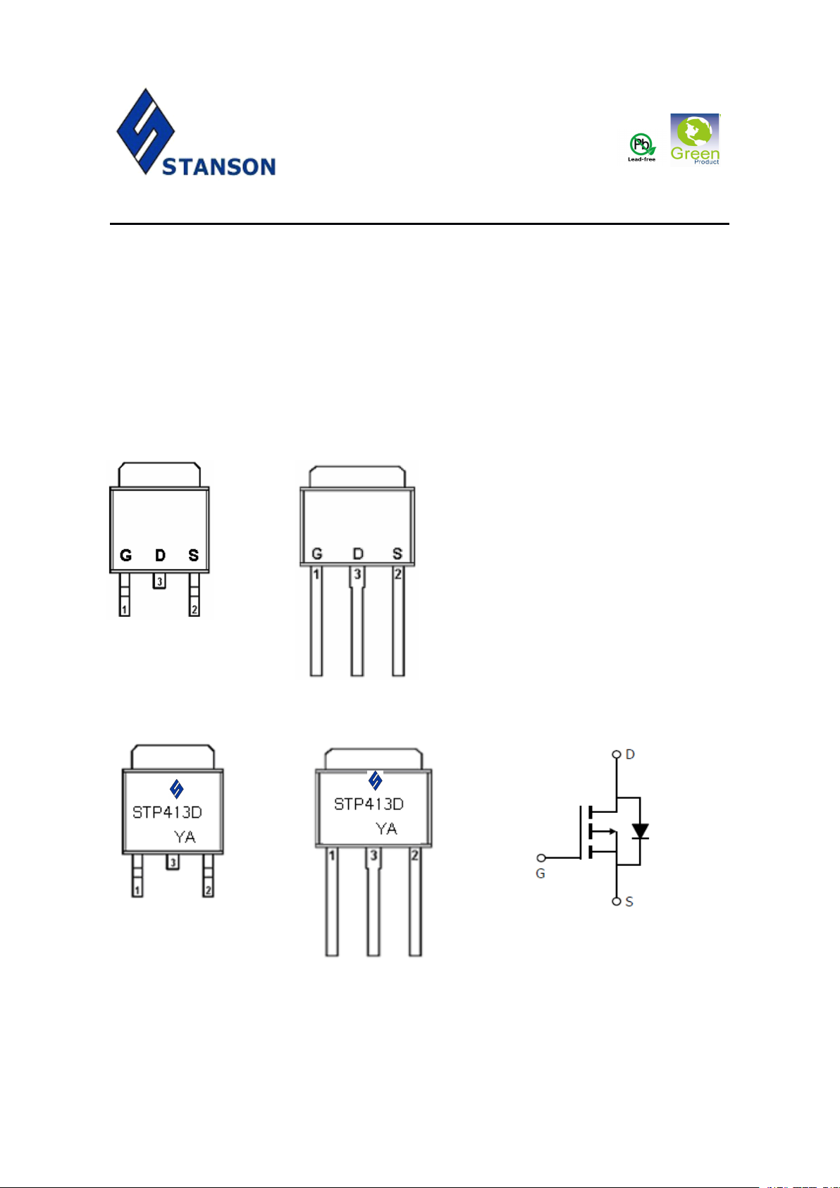
STP413D is the P-Channel logic enhancement mode power field effect transistor which
is produced using high cell density, DMOS trench technology. The STP413D has been
designed specially to improve the overall efficiency of DC/DC converters using either
synchronous or conventional switching PWM controllers. It has been optimized for low
gate charge, low R
PIN
CONFIGURATION
PIN
CONFIGURATION
PIN
PIN CONFIGURATION
CONFIGURATION (D-PAK)
DS(ON)
and fast switching speed.
(D-PAK)
(D-PAK)
(D-PAK)
TO-252
TO-252
TO-252
TO-252 TO-251
PART
PART
PART
PART MARKING
MARKING
MARKING
MARKING
TO-251
TO-251
TO-251
�
�
�
�
�
Y:
Year
Y:
Y:
Y: Year
STANSON TECHNOLOGY
120 Bentley Square, Mountain View, Ca 94040 USA
www.stansontech.com
Code
Year
Code
Year Code
Code A:
A:
Process
A:
Process
A: Process
Process Code
Code
Code
Code
Copyright © 200 9 , Stanson Corp.
STP413D 2009. V1
STP413D
STP413D
STP413D
STP413D
P Channel Enhancement Mode MOSFET
-
12.0 A
ABSOULTE
Parameter
Parameter
Parameter
Parameter
Symbol
Symbol
Symbol
Symbol
Typical
Typical
Typical
Typical
Unit
Unit
Unit
Unit
Drain-Source Voltage
VDSS
-4 0
V
Gate-Source Voltage
VGSS
± 20
V
Continuous Drain Current (TJ=150
℃
)
TA=25 ℃
TA=70
℃
ID
-12.0
-10.0
A
Pulsed Drain Current
IDM
- 30
A
Continuous Source Current (Diode Conduction)
IS
-1 2
A
Power Dissipation
TA=25 ℃
TA=70
℃
PD
50
25
W
Operation Junction Temperature
TJ
150
℃
Storgae Temperature Range
TSTG
-55/150
℃
Thermal Resistance-Junction to Ambient
R θ JA
6 0
℃
/W
ABSOULTE
ABSOULTE
ABSOULTE MAXIMUM
MAXIMUM
MAXIMUM
MAXIMUM RATINGS
RATINGS
RATINGS
RATINGS (Ta = 25
℃
Unless otherwise noted )
STANSON TECHNOLOGY
120 Bentley Square, Mountain View, Ca 94040 USA
www.stansontech.com
Copyright © 200 9 , Stanson Corp.
STP413D 2009. V1
STP413D
STP413D
STP413D
STP413D
P Channel Enhancement Mode MOSFET
-
12.0 A
ELECTRICAL
Parameter
Parameter
Parameter
Parameter
Symbol
Symbol
Symbol
Symbol
Condition
Condition
Condition
Condition
Min
Min
Min
Min
Typ
Typ
Typ
Typ
Max
Max
Max
Max
Uni
Uni
Uni
Uni
t
t
t
t
Static
Static
Static
Static
Drain-Source
Breakdown Voltage
V
(BR)DSSVGS
=0V,ID= -250u A
-4 0
V
Gate Threshold
Voltage
V
GS(th)
V
DS
=V
GS
,ID= -2 50uA
-0.8
-2.5
V
Gate Leakage Current
I
GSSVDS
=0V,V
GS
= ± 20V
± 100
nA
Zero Gate Voltage
Drain Current
I
DSS
V
DS
= -40 V,V
GS
=0V
- 1
uA
V
DS
= -40 V,V
GS
=0V
TJ= 5 5 ℃
-5
On-State Drain
Current
I
D(on)
V
DS
≧
-10 V,V
D S
= -5V
-30
A
Drain-source OnResistance
R
DS(on)
V
GS
= - 10V,ID=-12 A
V
GS
= -4.5 V,ID= -8 A
365241
57
m Ω
Forward
Transconductance
gfs
V
DS
= - 5V,ID= -12A
23
S
Diode Forward Voltage
VSDIS= -1.0 A,V
GS
=0V
- 1.2VDynamic
Dynamic
Dynamic
Dynamic
Total Gate Charge
Q
g
V
DS
= -10 V,V
DS
= -20V
ID=-12A
16.5
nC
Gate-Source Charge
Qgs3.8
Gate-Drain Charge
Q
gd
3.5
Input Capacitance
C
iss
V DS = -20 V,VGS=0V
F=1MHz
900
pF
Output Capacitance
C
oss
69
Reverse
Transfer C apacitance
C
rss
115
Turn-On Time
t
d(on)
tr
V
GS
= -10 V,V
DS
= -20 V
RL= 1.6 Ω ,R
GEN
= 3 Ω
6.9
nS
9
Turn-Off Time
t
d(off)
tf
44.8
41.2
ELECTRICAL
ELECTRICAL
ELECTRICAL CHARACTERISTICS
CHARACTERISTICS
CHARACTERISTICS
CHARACTERISTICS ( Ta = 25
℃
Unless otherwise noted )
STANSON TECHNOLOGY
120 Bentley Square, Mountain View, Ca 94040 USA
www.stansontech.com
Copyright © 200 9 , Stanson Corp.
STP413D 2009. V1
STP413D
STP413D
STP413D
STP413D
P Channel Enhancement Mode MOSFET
-
12.0 A
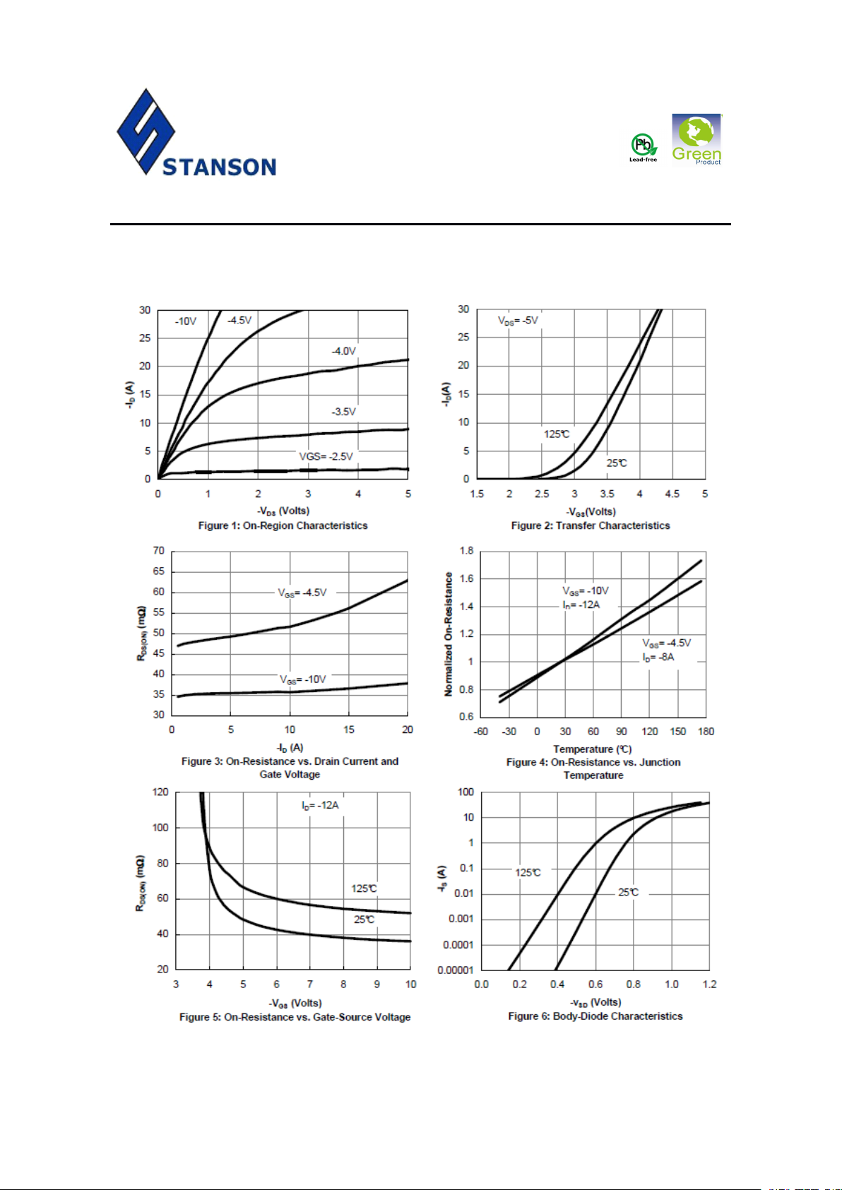
TYPICAL
TYPICAL
TYPICAL
TYPICAL CHARACTERICTICS
CHARACTERICTICS
CHARACTERICTICS
CHARACTERICTICS
STANSON TECHNOLOGY
120 Bentley Square, Mountain View, Ca 94040 USA
www.stansontech.com
Copyright © 200 9 , Stanson Corp.
STP413D 2009. V1
 Loading...