

Stanson STP3467 Schematic [ru]
STP3467
STP3467
STP3467
STP3467
PChannelEnhancementModeMOSFET
-5.2A
DESCRIPTION
Part
Part
Part
PartNumber
N umber
Number
Number
Package
Package
Package
Package
Part
Part
Part
PartMarking
M arking
Marking
Marking
STP3467ST6RG
TSOP-6
67YW
FEATUR
FEATUR
FEATUR
FEATURE
E
E
E
◆-20V/-5.0A,RDS(ON)=90mohm@VGS=-4.5V
◆-20V/-3.5A,RDS(ON)=110mohm@VGS=-2.5V
◆-20V/-1.7A,RDS(ON)=140mohm@VGS=-1.8V
◆Superhighdensitycelldesignforextremelylow
RDS(ON)
◆Exceptionalan-resistanceandmaximumDC
currentcapability
◆TSOP-6Ppackagedesign
67YW
DSD
DDG
DESCRIPTION
DESCRIPTION
DESCRIPTION
TheSTP3467istheP-Channelenhancementmodepowerfieldeffecttransistorwhichis
producedusinghighcelldensity,DMOStrenchtechnology.Thishighdensityprocessis
especiallytailoredtominimizeon-stateresistance.Thesedevicesareparticularly
suitedforlowvoltageapplication,suchascellularphoneandnotebookcomputer
powermanagementandotherbatterypoweredcircuits,andlowin-linepowerlossare
neededinaverysmalloutlinesurfacemountpackage.
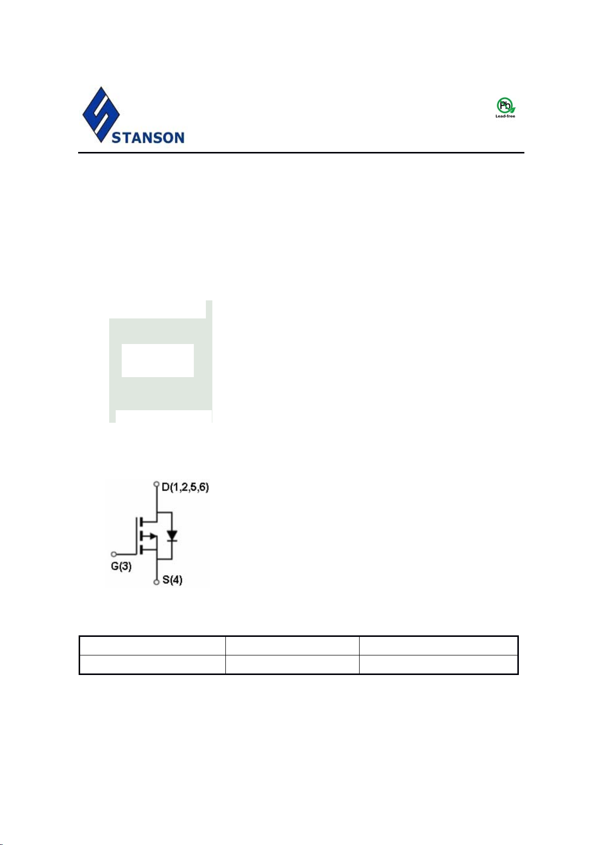
P IN
C ONFIGURATION
PIN
CONFIGURATION
PIN
PINCONFIGURATION
CONFIGURATION
TS
O P-
OP-
OP-6P
6 P
6P
6P
Y:
Y:
Y:
Y:Year
A:
A:
A:
A:Week
Y ear
Year
Year
W eek
Week
WeekCode
C ode
Code
Code
TS
TS
TSOP-
ORDERING
ORDERING
ORDERING
ORDERINGINFORMATION
STANSONTECHNOLOGY
120BentleySquare,MountainView,Ca94040USA
http://www.stansontech.com
※WeekCodeCode:A~Z;a~z
※STP3467ST6RGST6:TSOP-6;R:TapeReel;G:Pb–Free
I NFORMATION
INFORMATION
INFORMATION
STP34672008.V1
STP3467
STP3467
STP3467
STP3467
PChannelEnhancementModeMOSFET
-5.2A
ABSOULTE
Parameter
Parameter
Parameter
Parameter
Symbol
Symbol
Symbol
Symbol
Typical
Typical
Typical
Typical
Unit
Unit
Unit
Unit
Drain-SourceVoltage
V
DSS
-20
V
Gate-SourceVoltage
V
GSS
±12
V
ContinuousDrainCurrent(TJ=150℃)
TA=25℃
TA=70℃
I
D
-5.2
-4.2
A
PulsedDrainCurrent
I
DM
-20
A
ContinuousSourceCurrent(DiodeConduction)
I
S
-1.7
A
PowerDissipation
TA=25℃
P
D
2.0
W
TA=70℃
1.3
OperationJunctionTemperature
T
J
-55/150
℃
StorageTemperatureRange
T
STG
-55/150
℃
ThermalResistance-JunctiontoAmbient
R
θJA
90
℃/W
ABSOULTE
ABSOULTE
ABSOULTEMAXIMUM
M AXIMUM
MAXIMUM
MAXIMUMRATINGS
R ATINGS
RATINGS
RATINGS(Ta=25℃unlessotherwisenoted)
STANSONTECHNOLOGY
120BentleySquare,MountainView,Ca94040USA
http://www.stansontech.com
STP34672008.V1
STP3467
STP3467
STP3467
STP3467
PChannelEnhancementModeMOSFET
-5.2A
ELECTRICAL
Parameter
Parameter
Parameter
Parameter
Symbol
Symbol
Symbol
Symbol
Condition
Condition
Condition
Condition
Min
Min
Min
Min
Typ
Typ
Typ
Typ
Max
Max
Max
Max
Unit
Unit
Unit
Unit
Static
Static
Static
Static
Drain-SourceBreakdown
Voltage
V
(BR)DSS
V
GS
=0V,ID=-250uA
-20
V
GateThresholdVoltage
V
GS(th)
V
DS
=VGS,ID=-250uA
-0.35
-0.8
V
GateLeakageCurrent
I
GSS
V
DS
=0V,V
GS
=
±12
V
±
100
nA
ZeroGateVoltageDrain
Current
I
DSS
V
DS
=-20V,V
GS
=0V
-1
uA
V
DS
=-20V,V
GS
=0V
TJ=55℃
-5
On-StateDrainCurrent
I
D(on)VDS
≦-5V,V
GS
=-10V
-6
A
Drain-sourceOn-Resistance
R
DS(on)
V
GS
=-10V,ID=-5.2A
0.075
0.090
Ω
V
GS
=-4.5V,ID=-4.2A
0.090
0.110
V
GS
=-1.8V,ID=-1.7A
0.120
0.140
ForwardTransconductance
g
fs
V
DS
=-5.0V,ID=-2.8A
-10
S
DiodeForwardVoltage
V
SD
IS=-1.5A,V
GS
=0V
-0.8
-1.2
V
Dynamic
Dynamic
Dynamic
Dynamic
TotalGateCharge
Qg4.8
8
nC
Gate-SourceCharge
Qgs1.0
Gate-DrainCharge
Qgd1.0
InputCapacitance
Ciss
V
DS
=-6V,V
GS
=0,
f=1MHz
485
pF
OutputCapacitance
Coss
85
ReverseTransfer
Capacitance
Crss
40
Turn-OnTime
T
d(on)
V
DD
=-6V,
RL=6Ω,V
GEN
=-4.5V
RG=6Ω
10
15
ns
tr15
25
Turn-OffTime
T
d(off)
18
25
tf15
20
V
DS
=-6V,V
GS
=-4.5V,
V
DS
=-2.8A
ELECTRICAL
ELECTRICAL
ELECTRICALCHARACTERISTICS
C HARACTERISTICS
CHARACTERISTICS
CHARACTERISTICS(Ta=25℃Unlessotherwisenoted)
STANSONTECHNOLOGY
120BentleySquare,MountainView,Ca94040USA
http://www.stansontech.com
STP34672008.V1
 Loading...