

Stanson STN6303 Schematic [ru]
STN6303
53YW
Dual N Channel Enhancement Mode MOSFET
1.0A
DESCRIPTION
STN6303 is the dual N-Channel enhancement mode power field effect transistor which
is produced using high cell density, DMOS trench technology. This high density process
is especially tailored to minimize on-state resistance and provide superior switching
performance. These devices are particularly suited for low voltage applications such as
notebook computer circuits where high-side switching, low in-line power loss and
resistance to transients are needed.
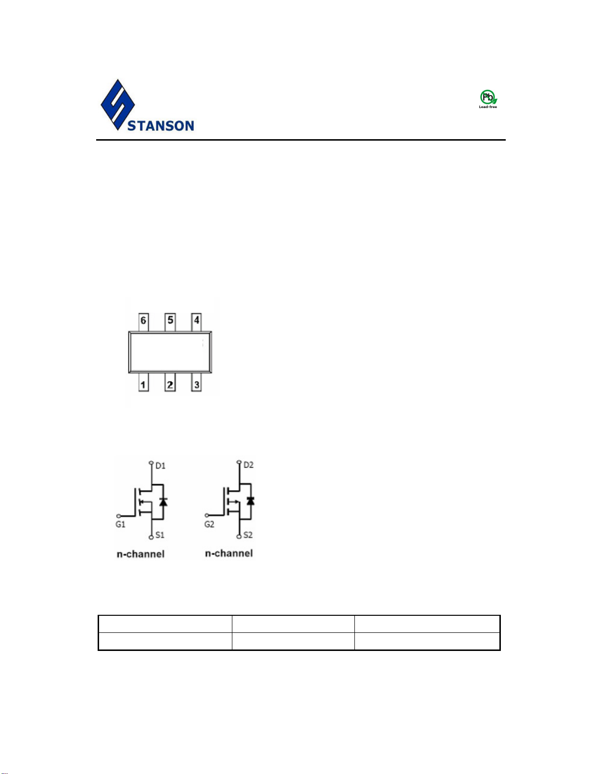
PIN CONFIGURATION
SOT-363 / SC70-6L
D1 G2 S2
FEATURE
23V/0.5A, R
23V/0.75A, R
Super high density cell design for extremely
low R
Exceptional low on-resistance and maximum
SOT-363 / SC70-6L package design
DS(ON)
DC current capability
= 400m-ohm@VGS =4.5V
DS(ON)
=550m-ohm@VGS =2.5V
DS(ON)
S1 G D2
Y: Year
W: Process Code
ORDERING INFORMATION
Part Number Package Part Marking
STN6303 SOT-363 / SC70-6L 53
※ Process Code : A ~ Z(1~26) ; a ~ z(27~52)
STANSON TECHNOLOGY
120 Bentley Square, Mountain View, Ca 94040 USA
http://www.stansontech.com
STN6303 2008. V1
STN6303
Dual N Channel Enhancement Mode MOSFET
ABSOULTE MAXIMUM RATINGS (Ta = 25 Unless otherwise noted )℃
Parameter Symbol
Typical Unit
1.0A
Drain-Source Voltage V
Gate-Source Voltage V
TA=25℃
(TJ=150 )℃
Pulsed Drain Current IDM 2.5 A
Continuous Source Current (Diode Conduction) IS 0.6 A
Operation Junction Temperature TJ -55/150 ℃
Storage Temperature Range T
Ambient
TA=70℃
TA=25℃
TA=70℃
T≦10sec
Steady State
23 V
DSS
+/-20
GSS
ID
PD
-55/150 ℃
STG
R
θJA
1.0 Continuous Drain Current
0.6
0.35 Power Dissipation
0.19
360 Thermal Resistance-Junction to
400
V
A
W
/W℃
STANSON TECHNOLOGY
120 Bentley Square, Mountain View, Ca 94040 USA
http://www.stansontech.com
STN6303 2008. V1
STN6303
Dual N Channel Enhancement Mode MOSFET
1.0A
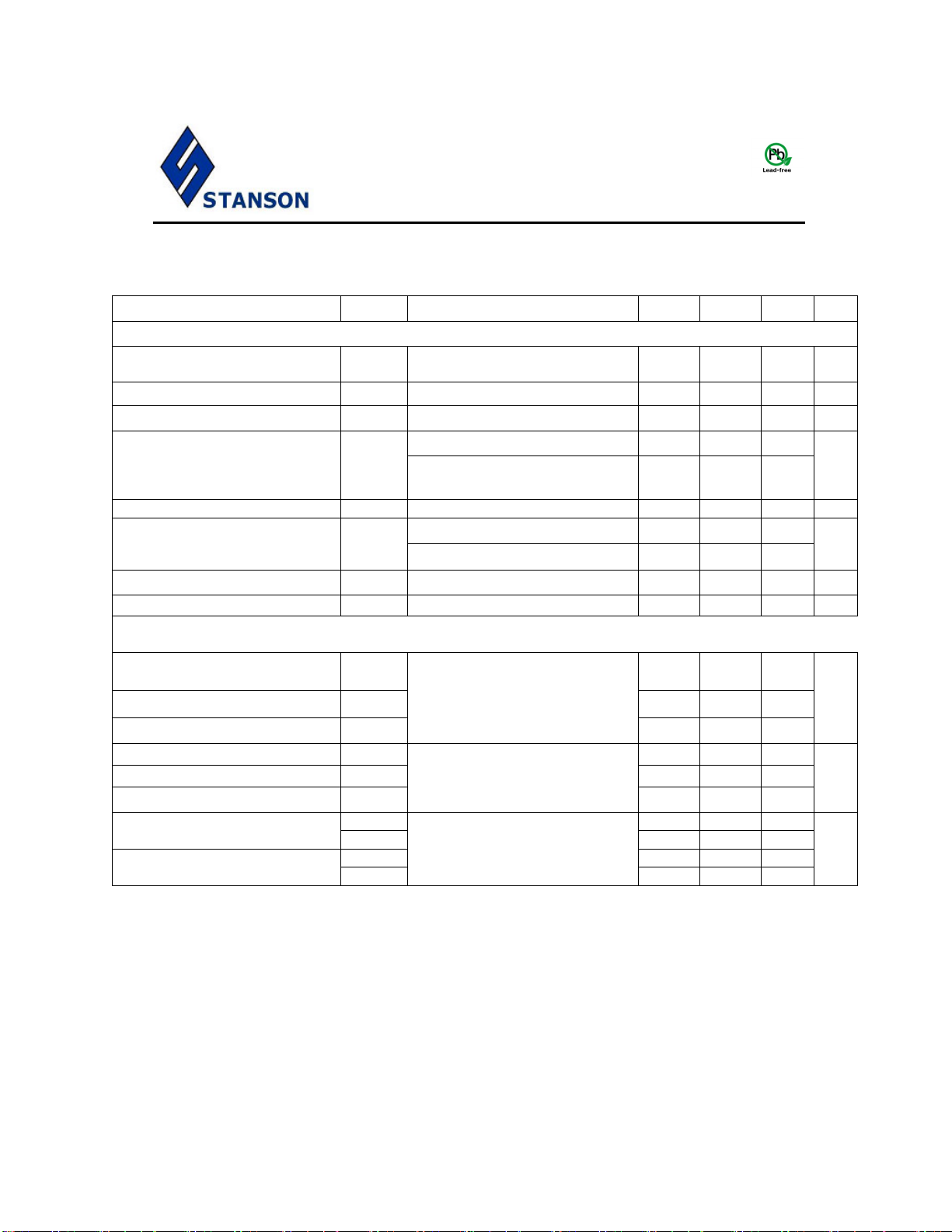
ELECTRICAL CHARACTERISTICS ( Ta = 25 Unless otherwise noted )℃
Parameter Symbol
OFF CHARACTERISTICS
Drain-Source Breakdown
V
(BR)DSS
Voltage
Gate Threshold Voltage V
Gate Leakage Current I
GS(th)
GSS
Zero Gate Voltage Drain
I
DSS
Current
On-State Drain Current I
V
D(on)
Drain-source On-Resistance R
DS(on)
Forward Transconductance gfs
Diode Forward Voltage VSD
DYNAMIC
Total Gate Charge Qg 1.2 1.5
Gate-Source Charge Qgs 0.2
VDS=10V,VGS=4.5V,VDS=0.7A
Gate-Drain Charge Qgd
Input Capacitance C
Output Capacitance C
Reverse Transfer Capacitance C
110
iss
34
oss
rss
T
5 10 Turn-On Time
d(on)
tr 8 15
T
d(off)
VDD=10V, RL=10Ω, ID=1.0A,
10 18 Turn-Off Time
tf
STANSON TECHNOLOGY
120 Bentley Square, Mountain View, Ca 94040 USA
http://www.stansontech.com
Condition Min Typ Max Unit
VGS=0V,ID=250uA
VDS=VGS,ID=250uA
23 V
0.35 1.0 V
VDS=0V,VGS=+/-12V
VDS=20V,VGS=0V
VDS=20V,VGS=0V
5
TJ=85℃
5V,VGS=4.5V 2.5 A
≦
DS
VGS=4.5V,ID=0.5A
VGS=2.7V,ID=0.2A
VDS=10V,ID=1.2A
IS=0.5A,VGS=0V
385 400
530 550
2.6 S
0.8 1.2 V
0.3
VDS=10V,VGS=0V
f=1MHz
16
VGEN=4.5V, RG=6Ω
1.2 2.8
±100 nA
1
uA
mΩ
nC
pF
nS
STN6303 2008. V1
 Loading...