

Stanson STN4546 Schematic [ru]
STN45
STN45
STN45
STN45 4
4
4
4 6
6
6
6
N Channel Enhancement Mode MOSFET
6 .0 A
DESCRIPTION
FEATURE
FEATURE
FEATURE
FEATURE
4 0V/ 10.0 A, R
DS(ON)
= 20 m Ω (Typ.)
@V GS = 10V
4 0V/ 8.0 A, R
DS(ON)
= 23 m Ω
@V GS = 4.5 V
4 0V/ 6.0 A, R
DS(ON)
= 27 m Ω
@V GS = 2.5 V
Super high density cell design for
extremely low R
DS(ON)
Exceptional on-resistance and
maximum DC current capability
SOP-8 package design
STN4 54 6
Y A
DESCRIPTION
DESCRIPTION
DESCRIPTION
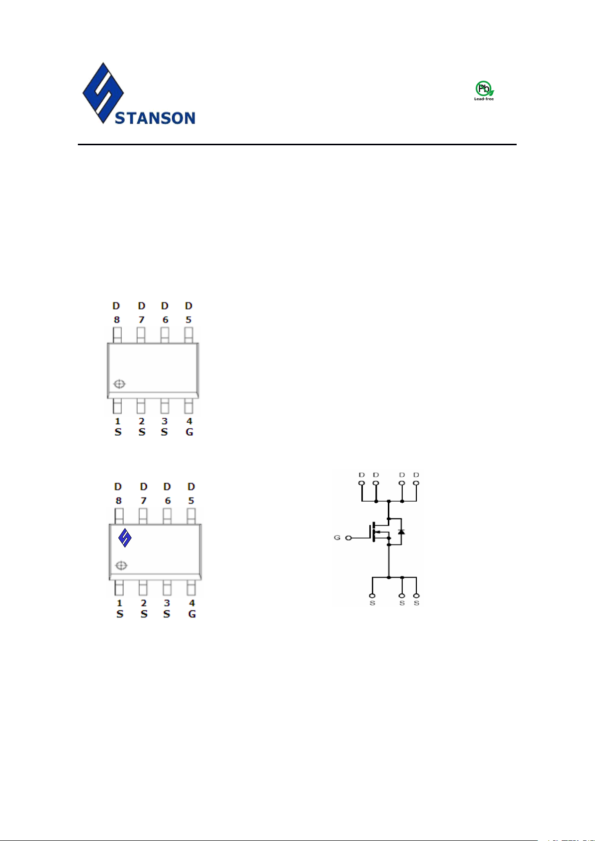
STN4526 is the N-Channel logic enhancement mode power field effect transistor
which is produced using high cell density, DMOS trench technology. This high density
process is especially tailored to minimize on-state resistance. These devices are
particularly suited for low voltage application such as power management and other
battery power ed circuits where high-side switching.
PIN
CONFIGURATION
PIN
CONFIGURATION
PIN
PIN CONFIGURATION
CONFIGURATION
SOP-8
SOP-8
SOP-8
SOP-8
�
�
�
�
�
�
PART
PART
PART
PART MARKING
Y:
Y:
Y:
Y: Year
STANSON TECHNOLOGY
120 Bentley Square, Mountain View, Ca 94040 USA
www.stansontech.com
MARKING
MARKING
MARKING
Year
Code
Year
Code
Year Code
Code A:
A:
Process
A:
Process
A: Process
Process Code
Code
Code
Code
Copyright © 2007, Stanson Corp.
STN45 4 6 200 9 . V1
STN45
STN45
STN45
STN45 4
4
4
4 6
6
6
6
N Channel Enhancement Mode MOSFET
6 .0 A
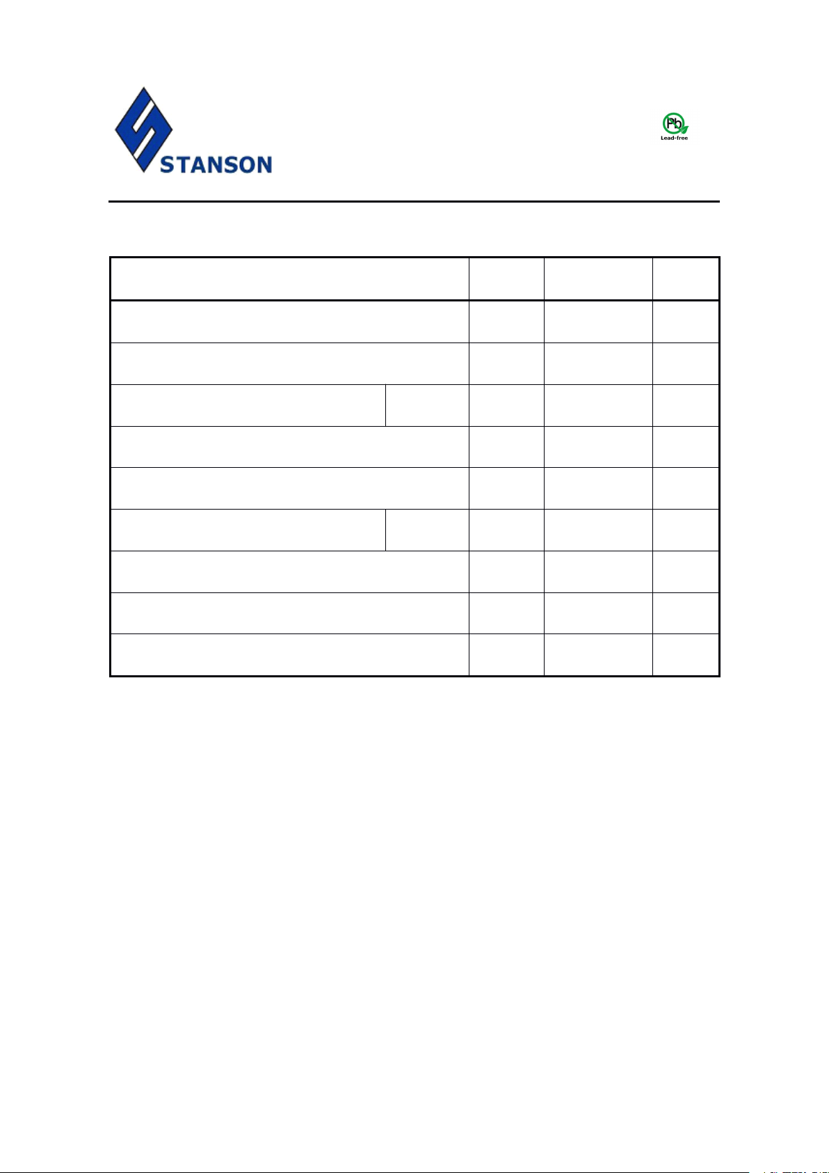
ABSOULTE
Parameter
Parameter
Parameter
Parameter
Symbol
Symbol
Symbol
Symbol
Typical
Typical
Typical
Typical
Unit
Unit
Unit
Unit
Drain-Source Voltage
VDSS
4 0
V
Gate-Source Voltage
VGSS
± 12
V
Continuous Drain Current (TJ=150
℃
)
TA=25 ℃
TA=70
℃
ID
6 .0
5 .0
A
Pulsed Drain Current
IDM30A
Continuous Source Current (Diode Conduction)
IS
2.3
A
Power Dissipation
TA=25 ℃
TA=70
℃
PD
2. 5
1.6
W
Operation Junction Temperature
TJ
-55/ 150
℃
Storgae Temperature Range
TSTG
-55/150
℃
Thermal Resistance-Junction to Ambient
R θ JA
8 0
℃
/W
ABSOULTE
ABSOULTE
ABSOULTE MAXIMUM
MAXIMUM
MAXIMUM
MAXIMUM RATINGS
RATINGS
RATINGS
RATINGS (Ta = 25
℃
Unless otherwise noted )
STANSON TECHNOLOGY
120 Bentley Square, Mountain View, Ca 94040 USA
www.stansontech.com
Copyright © 2007, Stanson Corp.
STN45 4 6 200 9 . V1
STN45
STN45
STN45
STN45 4
4
4
4 6
6
6
6
N Channel Enhancement Mode MOSFET
6 .0 A
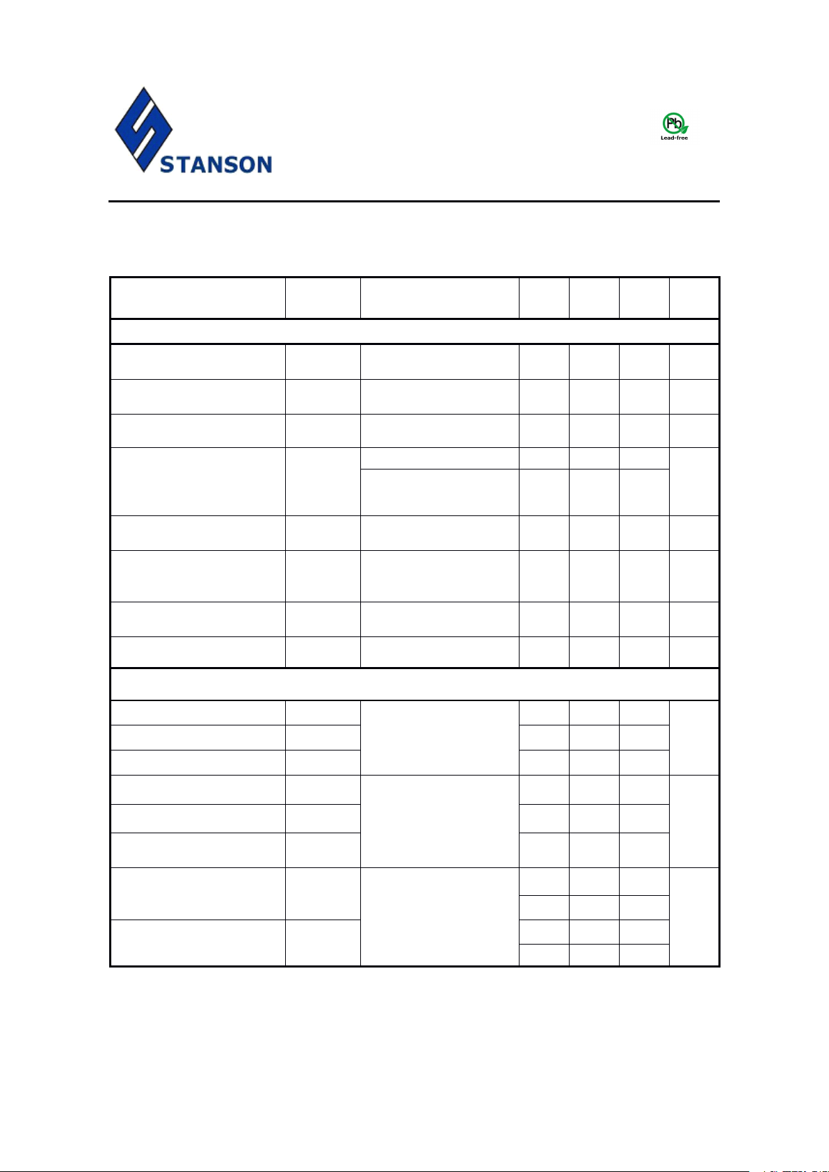
ELECTRICAL
Parameter
Parameter
Parameter
Parameter
Symbol
Symbol
Symbol
Symbol
Condition
Condition
Condition
Condition
Min
Min
Min
Min
Typ
Typ
Typ
Typ
Max
Max
Max
Max
Unit
Unit
Unit
Unit
Static
Static
Static
Static
Drain-Source
Breakdown Voltage
V
(BR)DSSVGS
=0V,ID=250uA
4 0
V
Gate Threshold
Voltage
V
GS(th)
V
DS
=V
GS
,ID= 2 50uA
0.5
1 . 2
V
Gate Leakage Current
I
GSSVDS
=0V,V
GS
= ± 12 V
± 100
nA
Zero Gate Voltage
Drain Current
I
DSS
V
DS
= 40 V,V
GS
=0V
1
uA
V
DS
= 40 V,V
GS
=0V
TJ=85 ℃
5
On-State Drain
Current
I
D(on)
V
DS
≧ 5V,V
GS
= 10V
10
A
Drain-source OnResistance
R
DS(on)
V
GS
=10V,ID= 6.0 A
V
GS
= 4.5 V,ID= 5.0 A
V
GS
= 2.5 ,ID= 4.5 A
40
47
72
48
5580m Ω
Forward
Transconductance
gfs
V
DS
=15V,ID= 6.2A V
13
S
Diode Forward Voltage
VSDIS=2.3A,V
GS
=0V
0.8
1.2
V
Dynamic
Dynamic
Dynamic
Dynamic
Total Gate Charge
Q
g
V
DS
= 15 V,V
GS
= 10V
I
D
≡
5 A
10
1 5
nC
Gate-Source Charge
Qgs1.6
Gate-Drain Charge
Q
gd
2.0
Input Capacitance
C
iss
V DS = 20 V,VGS=0V
F=1MHz
500
pF
Output Capacitance
C
oss
80
Reverse
Transfer C apacitance
C
rss
45
Turn-On Time
t
d(on)
tr
V
DD
= 15 V,RL= 15 Ω
ID= 1 .0 A,V
GEN
=10V
RG= 6 Ω
15
20
nS
6
12
Turn-Off Time
t
d(off)
tf
10
20
40
80
ELECTRICAL
ELECTRICAL
ELECTRICAL CHARACTERISTICS
CHARACTERISTICS
CHARACTERISTICS
CHARACTERISTICS ( Ta = 25
℃
Unless otherwise noted )
STANSON TECHNOLOGY
120 Bentley Square, Mountain View, Ca 94040 USA
www.stansontech.com
Copyright © 2007, Stanson Corp.
STN45 4 6 200 9 . V1
 Loading...