

Stanson ST7400 Schematic [ru]
2
2
DESCRIPTION
ST7400 is the N-Channel logic enhancement mode power field effect transistor which
is produced using high cell density, DMOS trench technology. This high density
process is especially tailored to minimize on-state resistance. These devices are
particularly suited for low voltage application such as cellular phone and notebook
computer power management, other battery powered circuits, and low in-line power
loss are required. The product is in a very small outline surface mount package.
ST7400
N Channel Enhancement Mode MOSFET
2.8A
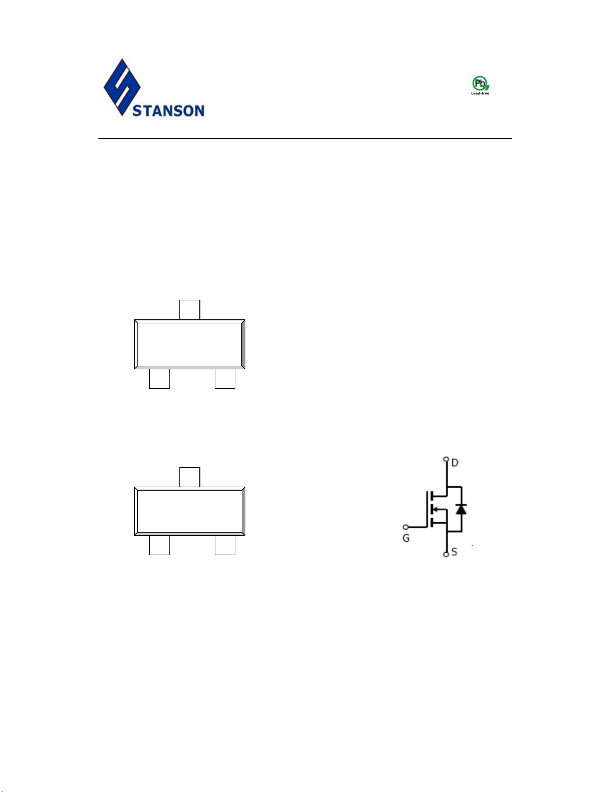
PIN CONFIGURATION
SOT-323 (SC-70)
3
D
G S
1
1.Gate 2.Source 3.Drain
PART MARKING
SOT-323
FEATURE
30V/2.8A, R
30V/2.5A, R
30V/1.5A, R
Super high density cell design for
Extremely low R
Exceptional on-resistance and
maximum DC current capability
SOT-323 (SC-70) package design
= 77mΩ
DS(ON)
@VGS =10V
= 85mΩ
DS(ON)
@VGS = 4.5V
= 170mΩ
DS(ON)
@VGS = 2.5V
DS(ON)
3
00YW
1
Y: Year Code A: Process Code
STANSON TECHNOLOGY
120 Bentley Square, Mountain View, Ca 94040 USA
http://www.stansontech.com
ST7400 2005. V1
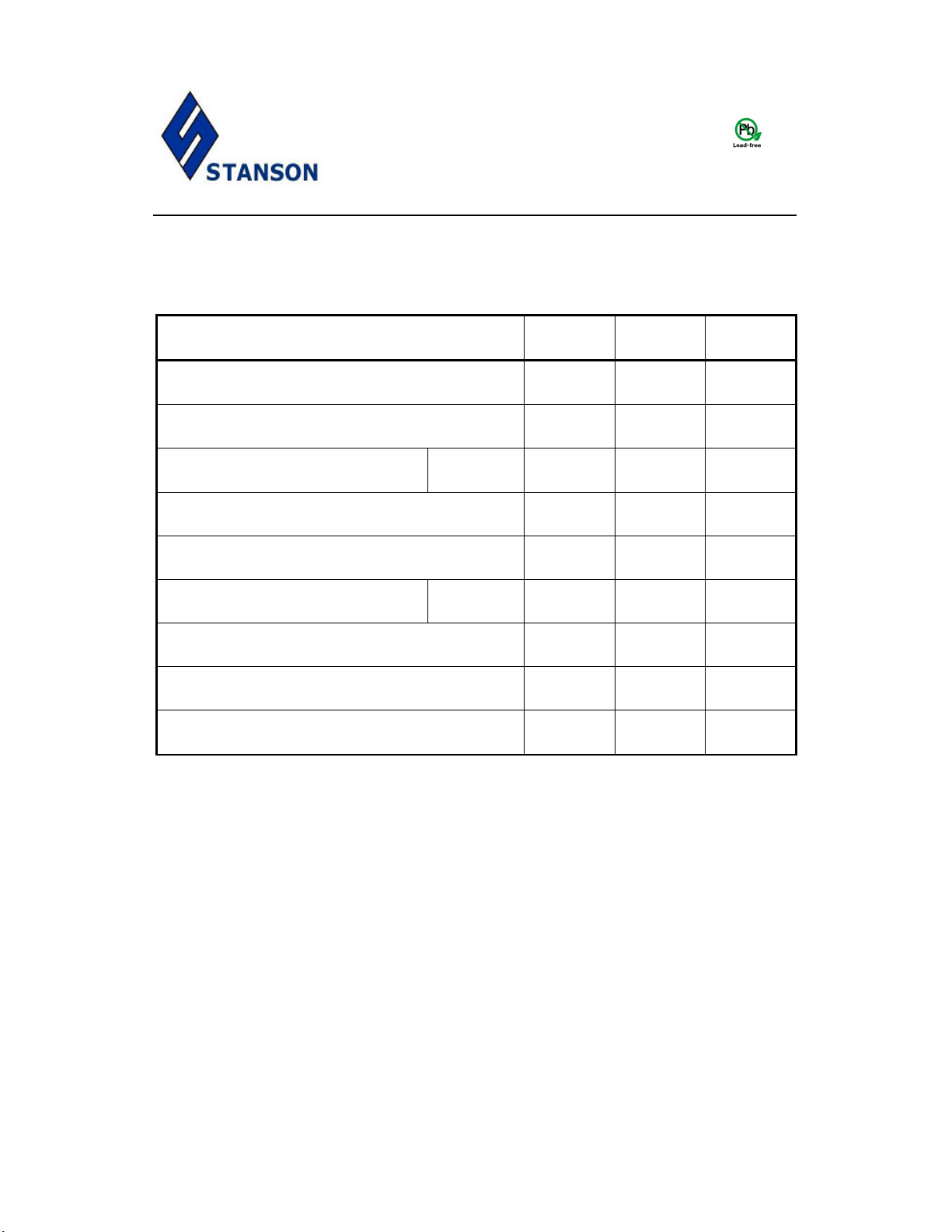
ABSOULTE MAXIMUM RATINGS (Ta = 25℃ Unless otherwise noted )
ST7400
N Channel Enhancement Mode MOSFET
Parameter Symbol Typical Unit
2.8A
Drain-Source Voltage V
Gate-Source Voltage V
Continuous Drain CurrentTJ=150℃)
Pulsed Drain Current IDM 10 A
Continuous Source Current (Diode Conduction) IS 1.25 A
Power Dissipation
Operation Junction Temperature TJ 150
Storage Temperature Range T
Thermal Resistance-Junction to Ambient
TA=25℃
TA=70℃
TA=25℃
TA=70℃
30 V
DSS
±
GSS
ID
PD
-55/150
STG
θ
R
JA
12
2.8
2.3
0.33
0.21
100
W
℃
℃
℃
STANSON TECHNOLOGY
120 Bentley Square, Mountain View, Ca 94040 USA
http://www.stansontech.com
V
A
/W
ST7400 2005. V1
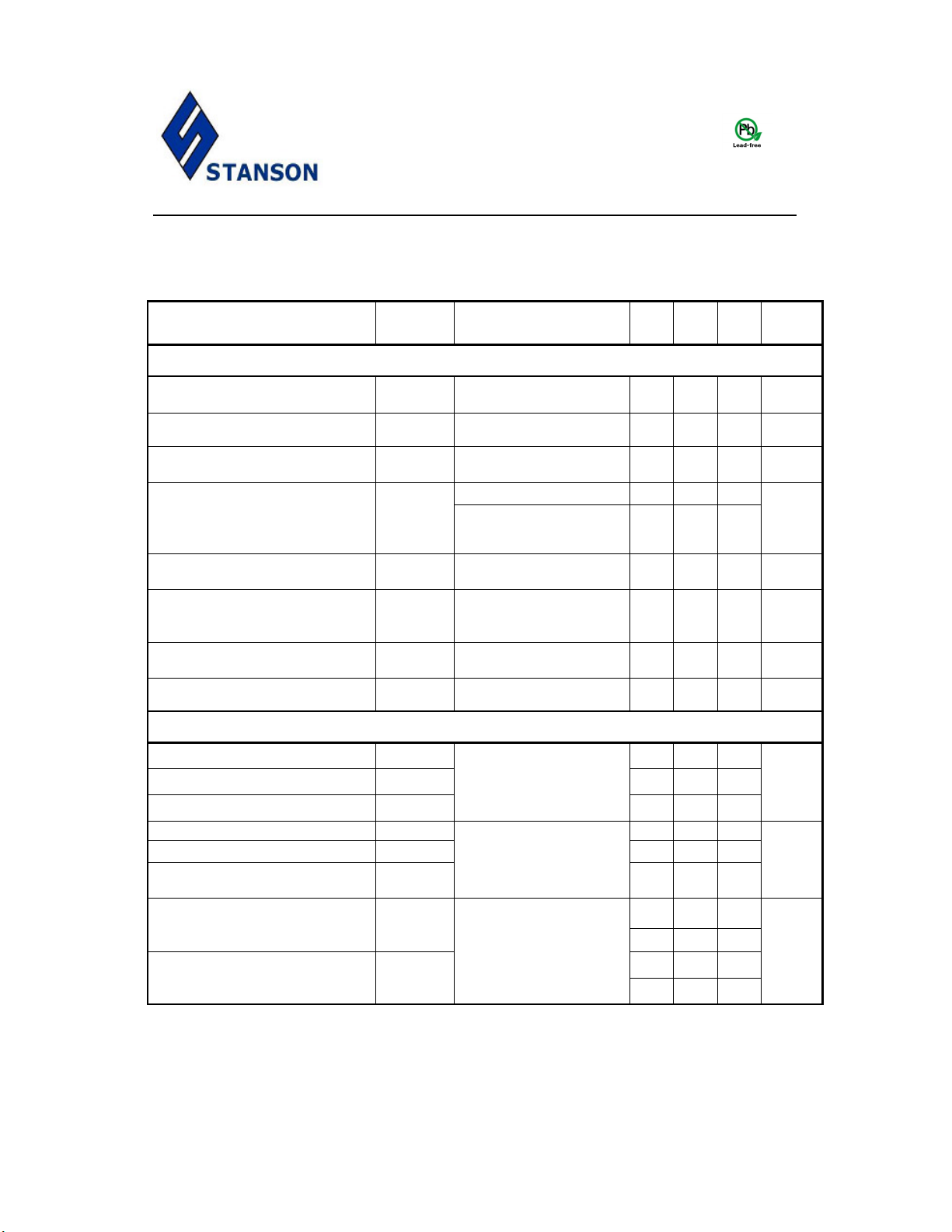
ST7400
N Channel Enhancement Mode MOSFET
ELECTRICAL CHARACTERISTICS ( Ta = 25℃ Unless otherwise noted )
2.8A
Parameter Symbol
Condition Min Typ Max Unit
Static
Drain-Source Breakdown
Voltage
Gate Threshold Voltage V
Gate Leakage Current I
V
(BR)DSS
GS(th)
GSS
VGS=0V,ID=250uA 30
VDS=VGS,ID=250uA 0.8
VDS=0V,VGS=±12V
V
1.6
±
100
V
nA
VDS=24V,VGS=0V 1
Zero Gate Voltage Drain
Current
On-State Drain Current I
Drain-source On-Resistance R
I
DSS
D(on)
DS(on)
VDS=24V,VGS=0V
≦
V
DS
-5V,VGS=-4.5V
VGS=10V,ID=2.8A
VGS=4.5V,ID=2.3A
VGS=2.5V,ID=1.5A
TJ=85℃
4.0
62
70
95
5
77
85
110
uA
A
mΩ
Forward Transconductance gfs VDS=5V,ID=4.0V 4 S
Diode Forward Voltage VSD IS=1.0A,VGS=0V 0.8 1.2
V
Dynamic
Total Gate Charge Qg 4.2
Gate-Source Charge Qgs 0.6
Gate-Drain Charge Qgd
Input Capacitance C
Output Capacitance C
Reverse Transfer
Capacitance
Turn-On Time
Turn-Off Time
380
iss
55
oss
C
rss
t
d(on)
tr
t
d(off)
tf
VDS=15V
VGS=4.5V
ID-2.0A
VDS=15V
VGS=0V
F=1MHz
VDS=15V
ID=1A
RL=15Ω
RG=3Ω
V
=10V
GEN
1.5
40
2.5
2.5
20
5
nC
pF
nS
STANSON TECHNOLOGY
120 Bentley Square, Mountain View, Ca 94040 USA
http://www.stansontech.com
ST7400 2005. V1
 Loading...