

Page 1

UM1519
User manual
ZigBee® dual IF EEPROM adapter for the STM322xG-EVAL
Introduction
This user manual describes the ZigBee® adapter for the STM322xG-EVAL needed to
manage a smartplugW network system through the STM322xG-EVAL board. The ZigBee
adapter for the STM322xG-EVAL has been developed in order to interface the STM322xGEVAL board with the ZigBee coordinator. The ZigBee coordinator is connected to the
STM322xG demonstration board through the adapter that allows SPI, I²C and UART
communication. The user can properly set jumpers JP3 and JP4 in order to choose how to
communicate between the STM32W and STM32F2xx. The I²C interface is used for the
communication of the STM32W and the dual interface EEPROM onboard. In Figure 1, it is
possible to take a quick look at the STM322xG-Eval board and a smartplug node block
diagram. The dual interface EEPROM “M24LR64r” onboard is accessible from both the
STM32W and the STM32F2xx via I²C interface and remotely by means of an RF reader.
Therefore, it is possible to read and update parameters from inside (I²C) and outside (RF)
the application. It therefore allows final application data management:
■ IDentification: read-only unique identifier
■ Traceability: trace code, date, BOM code, etc.
■ Inventory: supply chain visibility
■ Live update: application parameter update
■ Remote activation: code enabler
■ Maintenance: wireless access to events/logs
■ Diagnostics: possible real-time wireless access to parameters
Figure 1. STM322xG-EVAL board and a smartplug node block diagram
September 2012 Doc ID 022813 Rev 2 1/40
www.st.com
Page 2

Contents UM1519
Contents
1 STM3220G-EVAL demonstration board . . . . . . . . . . . . . . . . . . . . . . . . . . 5
1.1 Features . . . . . . . . . . . . . . . . . . . . . . . . . . . . . . . . . . . . . . . . . . . . . . . . . . . 6
1.2 Hardware layout and configuration . . . . . . . . . . . . . . . . . . . . . . . . . . . . . . . 6
1.3 Power supply . . . . . . . . . . . . . . . . . . . . . . . . . . . . . . . . . . . . . . . . . . . . . . . 9
1.4 Boot option . . . . . . . . . . . . . . . . . . . . . . . . . . . . . . . . . . . . . . . . . . . . . . . . 11
1.5 Clock source . . . . . . . . . . . . . . . . . . . . . . . . . . . . . . . . . . . . . . . . . . . . . . . 11
1.6 Reset source . . . . . . . . . . . . . . . . . . . . . . . . . . . . . . . . . . . . . . . . . . . . . . 12
1.7 EEPROM . . . . . . . . . . . . . . . . . . . . . . . . . . . . . . . . . . . . . . . . . . . . . . . . . 12
1.8 Ethernet . . . . . . . . . . . . . . . . . . . . . . . . . . . . . . . . . . . . . . . . . . . . . . . . . . 12
1.9 SRAM . . . . . . . . . . . . . . . . . . . . . . . . . . . . . . . . . . . . . . . . . . . . . . . . . . . . 13
1.10 Development and debug support . . . . . . . . . . . . . . . . . . . . . . . . . . . . . . . 14
1.11 Display and input devices . . . . . . . . . . . . . . . . . . . . . . . . . . . . . . . . . . . . . 14
1.12 Daughterboard extension connector CN1, 2, 3 and CN4 . . . . . . . . . . . . . 15
1.13 Ethernet RJ45 connector CN7 . . . . . . . . . . . . . . . . . . . . . . . . . . . . . . . . . 22
1.14 JTAG debugging connector CN14 . . . . . . . . . . . . . . . . . . . . . . . . . . . . . . 22
1.15 Power connector CN18 . . . . . . . . . . . . . . . . . . . . . . . . . . . . . . . . . . . . . . 23
1.16 TFT LCD connector CN19 . . . . . . . . . . . . . . . . . . . . . . . . . . . . . . . . . . . . 23
2 ZigBee module SPZB32W1x2.1 . . . . . . . . . . . . . . . . . . . . . . . . . . . . . . . 24
3 Hardware requirements . . . . . . . . . . . . . . . . . . . . . . . . . . . . . . . . . . . . . 24
4 Board configuration . . . . . . . . . . . . . . . . . . . . . . . . . . . . . . . . . . . . . . . . 25
4.1 STM322xG-EVAL demonstration board setup . . . . . . . . . . . . . . . . . . . . . 25
4.2 STM322xG-EVAL and ZigBee adapter with M24LR64-r memory . . . . . . 25
5 Schematics . . . . . . . . . . . . . . . . . . . . . . . . . . . . . . . . . . . . . . . . . . . . . . . 27
6 References . . . . . . . . . . . . . . . . . . . . . . . . . . . . . . . . . . . . . . . . . . . . . . . . 38
7 Revision history . . . . . . . . . . . . . . . . . . . . . . . . . . . . . . . . . . . . . . . . . . . 39
2/40 Doc ID 022813 Rev 2
Page 3

UM1519 List of tables
List of tables
Table 1. Power related jumpers and solder bridges . . . . . . . . . . . . . . . . . . . . . . . . . . . . . . . . . . . . . 10
Table 2. Boot related switch . . . . . . . . . . . . . . . . . . . . . . . . . . . . . . . . . . . . . . . . . . . . . . . . . . . . . . . 11
Table 3. EEPROM related jumper and solder bridge . . . . . . . . . . . . . . . . . . . . . . . . . . . . . . . . . . . . 12
Table 4. Ethernet related jumpers and solder bridges . . . . . . . . . . . . . . . . . . . . . . . . . . . . . . . . . . . 12
Table 5. SRAM related jumpers . . . . . . . . . . . . . . . . . . . . . . . . . . . . . . . . . . . . . . . . . . . . . . . . . . . . 13
Table 6. LCD modules . . . . . . . . . . . . . . . . . . . . . . . . . . . . . . . . . . . . . . . . . . . . . . . . . . . . . . . . . . . 14
Table 7. Daughterboard extension connector CN1 . . . . . . . . . . . . . . . . . . . . . . . . . . . . . . . . . . . . . 15
Table 8. Daughterboard extension connector CN2 . . . . . . . . . . . . . . . . . . . . . . . . . . . . . . . . . . . . . 17
Table 9. Daughterboard extension connector CN3 . . . . . . . . . . . . . . . . . . . . . . . . . . . . . . . . . . . . . 18
Table 10. Daughterboard extension connector CN4 . . . . . . . . . . . . . . . . . . . . . . . . . . . . . . . . . . . . . 20
Table 11. Ethernet RJ45 connector CN7 . . . . . . . . . . . . . . . . . . . . . . . . . . . . . . . . . . . . . . . . . . . . . . 22
Table 12. JTAG debugging connector CN14 . . . . . . . . . . . . . . . . . . . . . . . . . . . . . . . . . . . . . . . . . . . 23
Table 13. ZigBee adapter pinout description . . . . . . . . . . . . . . . . . . . . . . . . . . . . . . . . . . . . . . . . . . . 25
Table 14. Document revision history . . . . . . . . . . . . . . . . . . . . . . . . . . . . . . . . . . . . . . . . . . . . . . . . . 39
Doc ID 022813 Rev 2 3/40
Page 4

List of figures UM1519
List of figures
Figure 1. STM322xG-EVAL board and a smartplug node block diagram . . . . . . . . . . . . . . . . . . . . . . 1
Figure 2. STM3220G-EVAL board . . . . . . . . . . . . . . . . . . . . . . . . . . . . . . . . . . . . . . . . . . . . . . . . . . . . 5
Figure 3. STM3220G-EVAL board hardware block diagram . . . . . . . . . . . . . . . . . . . . . . . . . . . . . . . . 7
Figure 4. STM3220G-EVAL demonstration board layout . . . . . . . . . . . . . . . . . . . . . . . . . . . . . . . . . . 8
Figure 5. ZigBee adapter layout description . . . . . . . . . . . . . . . . . . . . . . . . . . . . . . . . . . . . . . . . . . . . 9
Figure 6. Ethernet RJ45 connector CN7 . . . . . . . . . . . . . . . . . . . . . . . . . . . . . . . . . . . . . . . . . . . . . . 22
Figure 7. JTAG debugging connector CN14 . . . . . . . . . . . . . . . . . . . . . . . . . . . . . . . . . . . . . . . . . . . 22
Figure 8. Power supply connector CN18 . . . . . . . . . . . . . . . . . . . . . . . . . . . . . . . . . . . . . . . . . . . . . . 23
Figure 9. ZigBee and dual interface EEPROM adapter for STM322xG-EVAL . . . . . . . . . . . . . . . . . 27
Figure 10. STM3220-21-45-46G-EVAL . . . . . . . . . . . . . . . . . . . . . . . . . . . . . . . . . . . . . . . . . . . . . . . . 28
Figure 11. STM3220-21-45-46G-EVALMCU . . . . . . . . . . . . . . . . . . . . . . . . . . . . . . . . . . . . . . . . . . . . 29
Figure 12. STM3220-21-45-46G-EVALEthernet . . . . . . . . . . . . . . . . . . . . . . . . . . . . . . . . . . . . . . . . . 30
Figure 13. STM3220-21-45-46G-EVALLCD . . . . . . . . . . . . . . . . . . . . . . . . . . . . . . . . . . . . . . . . . . . . 31
Figure 14. LCD module with both SPI and 16-bit interface . . . . . . . . . . . . . . . . . . . . . . . . . . . . . . . . . 32
Figure 15. STM3220-21-45-46G-EVAL I/O peripherals . . . . . . . . . . . . . . . . . . . . . . . . . . . . . . . . . . . . 33
Figure 16. STM3220-21-45-46G-EVAL I/O_Expander . . . . . . . . . . . . . . . . . . . . . . . . . . . . . . . . . . . . 34
Figure 17. STM3220-21-45-46G-EVAL JTAG and trace . . . . . . . . . . . . . . . . . . . . . . . . . . . . . . . . . . . 35
Figure 18. STM3220-21-45-46G-EVALPower . . . . . . . . . . . . . . . . . . . . . . . . . . . . . . . . . . . . . . . . . . . 36
Figure 19. STM3220-21-45-46G-EVALExtension connector . . . . . . . . . . . . . . . . . . . . . . . . . . . . . . . . 37
4/40 Doc ID 022813 Rev 2
Page 5

UM1519 STM3220G-EVAL demonstration board
1 STM3220G-EVAL demonstration board
Figure 2. STM3220G-EVAL board
The STM3220G-EVAL demonstration board is a complete demonstration and development
platform for the STM32 F-2 series and includes an embedded STM32F207IGH6 highperformance ARM
The full range of hardware features on the board is provided to help the user evaluate all
peripherals (USB OTG HS, USB OTG FS, Ethernet, motor control, CAN, MicroSD card,
smartcard, USART, audio DAC, RS-232, IrDA, SRAM, MEMS, EEPROM… etc.) and
develop their own applications. Extension headers make it possible to easily connect a
daughterboard or wrapping board for specific applications.
The in-circuit ST-LINK tool can be easily used for JTAG and SWD interface debugging and
programming.
®
Cortex-M3 32-bit microcontroller with a cryptographic acceleration cell.
Doc ID 022813 Rev 2 5/40
Page 6

STM3220G-EVAL demonstration board UM1519
1.1 Features
● STM32F207IGH6 microcontroller
● 16 Mbit SRAM
● 1 Gbyte or more MicroSD card
● Boot from user Flash, system memory or SRAM
● Both ISO/IEC 14443 type A and B smartcards supported
2
● I
C compatible serial interface 8-Kbyte EEPROM, MEMS and I/O expander
● IEEE 802.3-2002 compliant Ethernet connector
● Two CAN 2.0 A/B channels on the same DB connector
● RS-232 communication
● IrDA transceiver
● USB OTG (HS and FS) with Micro-AB connector
● Inductor motor control connector
● I2S audio DAC, stereo audio jack for headset
● 3.2" 240x320 TFT color LCD with touchscreen
● 4 color LEDs
● Camera module and extension connector for ST camera plug-in
● Joystick with 4-direction control and selector
● Reset, wake-up, tamper and user button
● RTC with backup battery
● Extension connector for daughterboard or wrapping board
● JTAG, SW and trace debug support
● Embedded ST-LINK/V2
● Five 5 V power supply options: power jack, USB FS connector, USB HS connector,
ST-LINK/V2 or daughterboard
● MCU consumption measurement circuit.
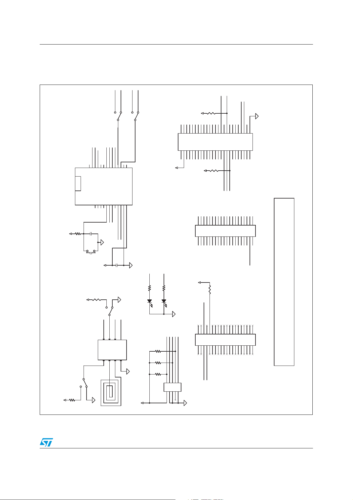
1.2 Hardware layout and configuration
The STM3220G-EVAL demonstration board is designed around the STM32F207IGH6
microcontroller with a cryptographic acceleration cell in the UFBGA176 package. The
hardware block diagram, Figure 2, illustrates the connection between the STM32F207IGH6
and peripherals (camera module, LCD, SRAM, EEPROM, MEMS, USART, IrDA, USB OTG
HS, USB OTG FS, Ethernet, audio, CAN bus, smartcard, MicroSD card and motor control)
and Figure 3 helps the user locate these features on the actual demonstration board.
6/40 Doc ID 022813 Rev 2
Page 7

UM1519 STM3220G-EVAL demonstration board
!-V
-2XXXXX6
34-&)'(
23
TRANSCEIVER
)R$!
TRANSCEIVER
3MARTCARD
INTERFACE
6REGULATOR
4&4,#$
-ICRO3$
CARD
!UDIO$!#
-#CONTROL
CONNECTOR
,%$S+EY
*4!'
-%-3
0OTENTIOMETER
3MARTCARD
CONNECTOR
)NTEGRATED2*
CONNECTOR
23
$"CONNECTOR
!$#
)3
'0)/
-))2-))
53!24
)#
%XTENSION
CONNECTORFOR
'0)/S
0(9
53!24
#!.
#!.
TRANSCEIVER
#!.
$"CONNECTOR
-#
3$)/
4RACE
$EBUG
/4'&3
53"-ICRO!"
CONNECTOR
%%02/-
)/EXPANDOR
*OYSTICK
4OUCHSCREEN
53"POWER
SWITCH
#!.
6REGULATOR
6REGULATOR
6REGULATOR
$#-)
#AMERA
MODULE
/4'(3
53"-ICRO!"
CONNECTOR
53"POWER
SWITCH
53"(3
0(9
$!#
&3-#
32!-
34,).+6
#AMERAEXTENSION
CONNECTOR
-ICROPHONE
!MPLIFIER
!UDIO*ACK
!$#
Figure 3. STM3220G-EVAL board hardware block diagram
Doc ID 022813 Rev 2 7/40
Page 8
STM3220G-EVAL demonstration board UM1519
!-V
#.
-OTORCONTROL
#.
-ICRO3$CARD
#.
4RACE
#.
*4!'
5
)R$!
#.
53" /4'&3
#.
53"/4'(3
#.
34,).+6
#.
#OLOR,#$
#.
#AMERAMODULE
#.
#AMERAEXTENSION
CONNECTOR
5
*OYSTICK
"
5SERKEY
"
4AMPER
#.
3MARTC ARD
"
7AKEUP
"
2ESET
26
0OTENTIOMETER
#.
6POW ERJAC K
#.
!UDIOJACK
#.
53!2 4
#.
#!.
5
34-&) '(
#.
2*
CONNECTOR
#.# .
%XTENSION
Figure 4. STM3220G-EVAL demonstration board layout
8/40 Doc ID 022813 Rev 2
Page 9

UM1519 STM3220G-EVAL demonstration board
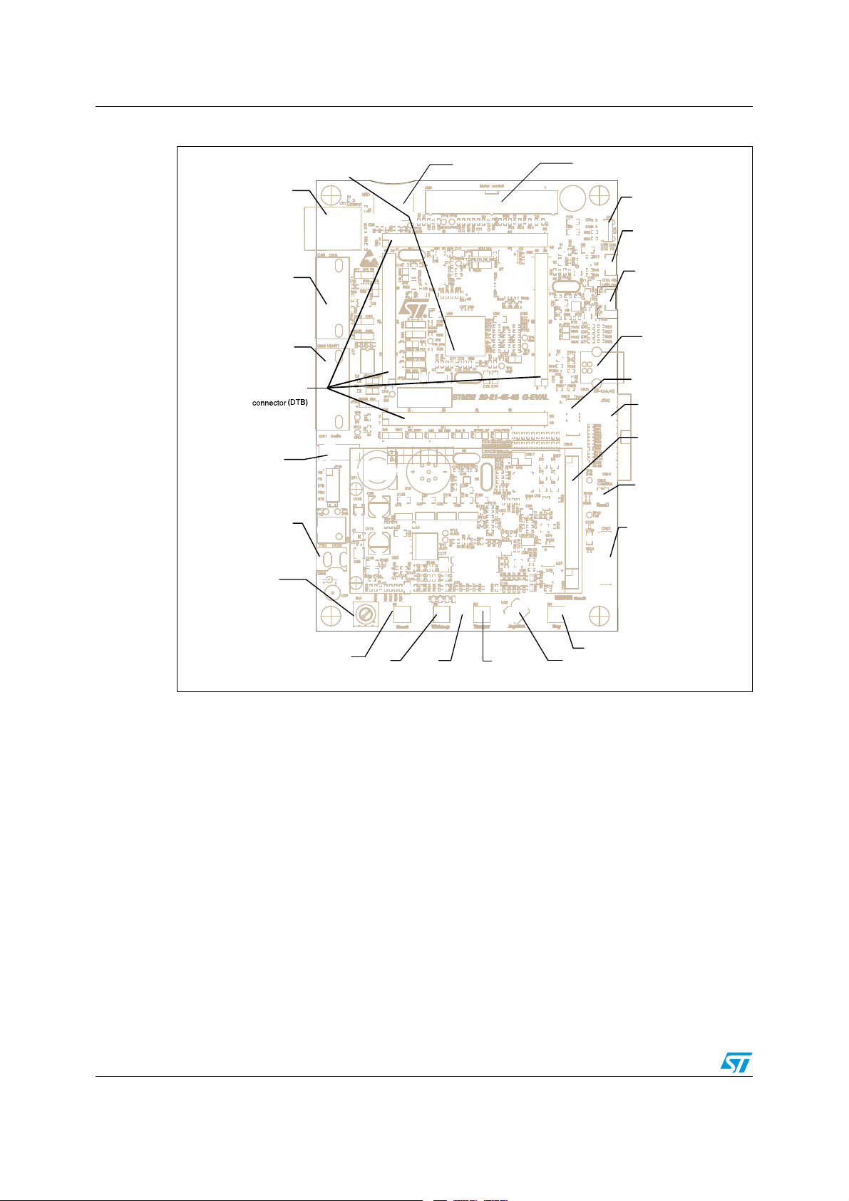
Figure 5. ZigBee adapter layout description
1.3 Power supply
The STM322xG-EVAL demonstration board is designed to be powered by 5 V DC power
supply and to be protected by PolyZen from a wrong power plug-in event. It is possible to
configure the demonstration board to use any of the following five sources for the power
supply:
● 5 V DC power adapter connected to JP18, the power jack on the board
● 5 V DC power with 500 mA limitation from CN8, the USB OTG FS Micro-AB connector
● 5 V DC power with 500 mA limitation from CN9, the USB OTG HS Micro-AB connector
● 5 V DC power with 500 mA limitation from CN21, the ST-LINK/V2 USB connector
● 5 V DC power from both CN1 and CN3, the extension connector for the daughterboard
(DTB for daughterboard on silkscreen).
The power supply is configured by setting the related jumpers JP4, JP32, JP18 and JP19,
as described in Ta bl e 1 .
Doc ID 022813 Rev 2 9/40
Page 10

STM3220G-EVAL demonstration board UM1519
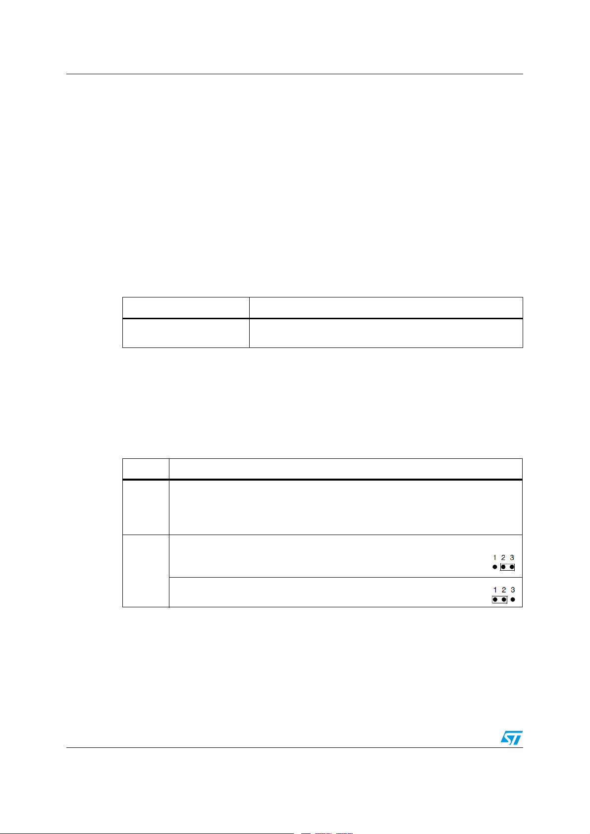
Table 1. Power related jumpers and solder bridges
Jumper Description
JP4
JP32
Jumper reserved for future use (RFU). It should be left open.
Default setting: not fitted
MCU_VDD is connected to 3.3 V power when JP32 is closed and MCU current
consumption measurement can be done manually by multi-meter when JP32 is
open.
Default setting: fitted
JP18 is used to select one of the four possible power supply resources.
To select the ST-LINK/V2 USB connector (CN21) power supply, set JP18 as shown:
(default setting)
For power supply jack (CN18) to the STM322xG-EVAL, JP18 is set as shown to the
right: (default setting)
To select daughterboard connector (CN1 and CN3) power
supply, set JP18 as shown:
JP18
To select USB OTG FS (CN8) power supply, set JP18 as shown:
To select USB OTG HS (CN9) power supply, set JP18 as shown:
To select power supply jack (CN18) power supply to both STM322xG-EVAL
and daughterboard connected on CN1 and CN3, set JP18 as shown
(daughterboard must not have its own power supply connected)
10/40 Doc ID 022813 Rev 2
Page 11

UM1519 STM3220G-EVAL demonstration board
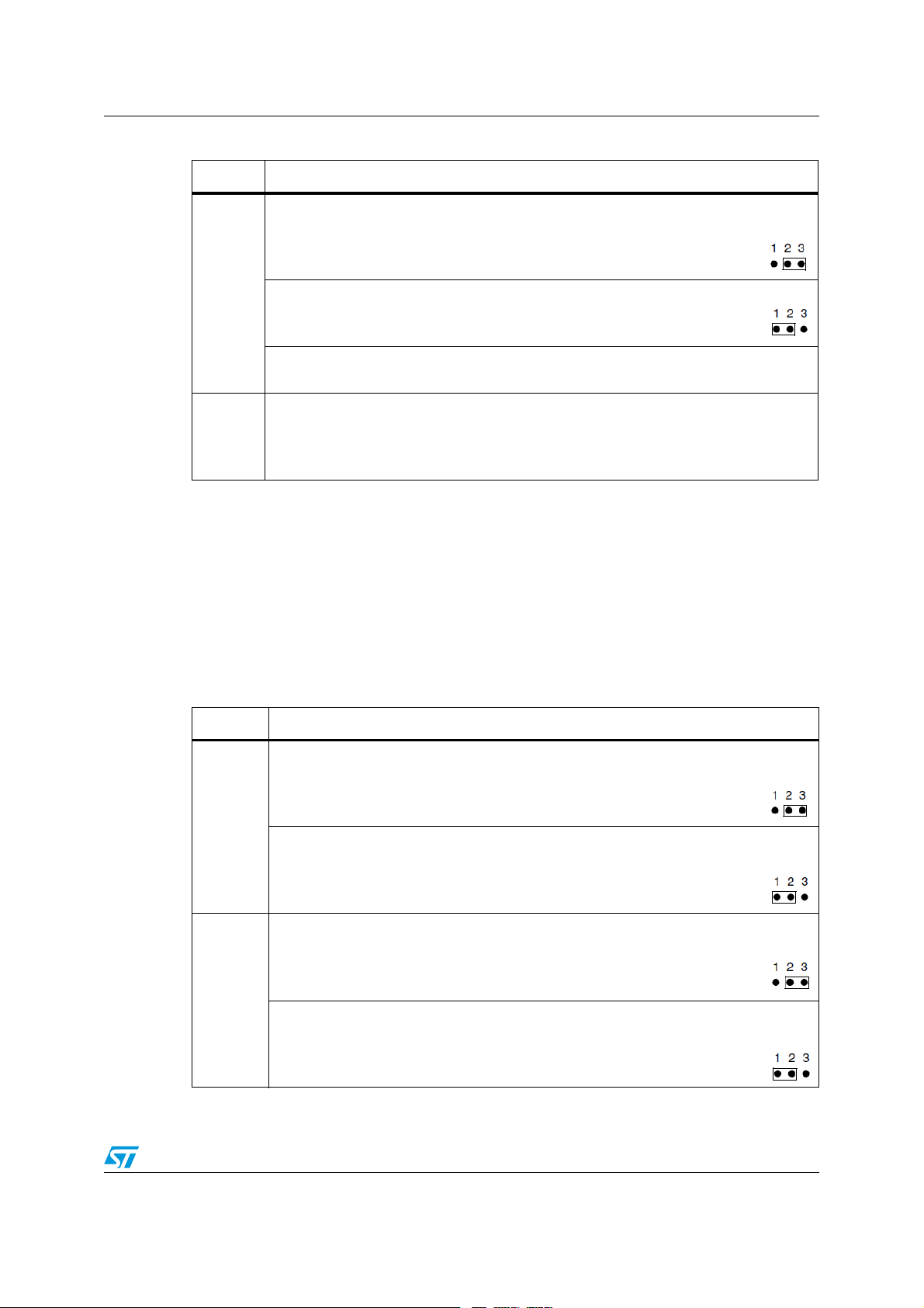
Table 1. Power related jumpers and solder bridges (continued)
Jumper Description
To connect Vbat to the battery, set JP19 as shown:
JP19
To connect Vbat to 3.3 V power, set JP19 as shown:
(default setting)
Note: The LED LD9 is lit when the STM322xG-EVAL demonstration board is correctly powered by
the 5 V.
1.4 Boot option
The STM322xG-EVAL demonstration board is able to boot from:
● Embedded user flash
● System memory with boot loader for ISP
● Embedded SRAM for debugging.
The boot option is configured by setting switch SW1 (BOOT1) and SW2 (BOOT0). The
BOOT0 can be configured also via RS232 connector CN16.
Table 2. Boot related switch
BOOT BOOT1 Boot source
0 Don’t care STM322xG-EVAL boots from user Flash (default setting)
1 1 STM322xG-EVAL boots from embedded SRAM
1 0 STM322xG-EVAL boots from system memory
1.5 Clock source
Four clock sources are available on the STM322xG-EVAL demonstration board for the
STM32F207IFT6 and RTC embedded.
● X1, 25 MHz crystal for Ethernet PHY with socket. It can be removed when clock is
provided by the MCO pin of the MCU
● X2, 26 MHz crystal for USB OTG HS PHY
● X3, 32 kHz crystal for embedded RTC
● X4, 25 MHz crystal with socket for the STM32F207IGH6 microcontroller (it can be
removed from socket when internal RC clock is used).
Doc ID 022813 Rev 2 11/40
Page 12
STM3220G-EVAL demonstration board UM1519
1.6 Reset source
The reset signal of the STM322xG-EVAL demonstration board is low active and the reset
sources include:
● Reset button B1
● Debugging tools from JTAG connector CN14 and trace connector CN13
● Daughterboard from CN3
● RS232 connector CN16 for ISP
● ST-LINK/V2.
1.7 EEPROM
A 64 Kbit EEPROM is connected to the I2C1 bus of the STM32F207IGH6.
Table 3. EEPROM related jumper and solder bridge
Jumper Description
1.8 Ethernet
The STM322xG-EVAL demonstration board supports 10M/100M Ethernet communication
by a PHY DP83848CVV (U5) and integrated RJ45 connector (CN7). Both MII and RMII
interfaces can be selected by setting jumpers JP5, JP6 and JP8 as listed below:
Table 4. Ethernet related jumpers and solder bridges
Jumper Description
JP8
JP6
JP24
JP8 is used to select MII or RMII interface mode.
To enable MII, JP8 is not fitted.
To enable RMII interface mode, JP8 is fitted.
Default setting: not fitted
To enable MII interface mode, set JP6 as shown (default setting):
To enable RMII interface mode, set JP6 as shown:
The EEPROM is in write protection mode when JP24 is fitted.
Default setting: not fitted
12/40 Doc ID 022813 Rev 2
Page 13
UM1519 STM3220G-EVAL demonstration board
Table 4. Ethernet related jumpers and solder bridges (continued)
Jumper Description
To provide 25 MHz clock for MII or 50 MHz clock for RMII by
MCO at PA8, set JP5 as shown (default setting):
JP5
SB1
To provide 25 MHz clock by external crystal X1 (for MII interface
mode only) set JP5 as shown:
When clock is provided by external oscillator U3, JP5 must not be fitted
(default setting).
SB1 is used to select clock source only for RMII mode.
To connect the clock from MCO to RMII_REF_CLK, close SB1.
The resistor R212 must be removed in this case.
Default setting: open
Note: A test point (TP2) is available on the board for the PTP_PPS feature test.
The Ethernet PHYU5 can be powered down by regulating PB14.
1.9 SRAM
The 16 Mbit SRAM is connected to the FSMC bus of the STM32F207IGH6 which shares the
same I/Os with CAN1 bus. JP3 and JP10 must not be fitted for SRAM and LCD application.
Table 5. SRAM related jumpers
Jumper Description
JP1
JP2
Connect PE4 to SRAM as A20 by setting JP1 as shown (default
setting):
Connect PE4 to trace connector CN13 as TRACE_D1 by setting
JP1 as shown:
Connect PE3 to SRAM as A19 by setting JP2 as shown (default
setting):
Connect PE3 to trace connector CN13 as TRACE_D0 by setting
JP2 as shown:
Doc ID 022813 Rev 2 13/40
Page 14

STM3220G-EVAL demonstration board UM1519
1.10 Development and debug support
The version 2 of the ST-LINK, called ST-LINK/V2, is embedded on the board. This tool
allows onboard program loading and debugging of the STM32F using the JTAG or SWD
interface.
Third-party debug tools are also supported by the JTAG (CN14) or trace (CN13) connectors.
To communicate with the embedded ST-LINK/V2, a specific driver needs to be installed on
the PC. To download and install this driver, refer to the software and development tools page
for the STM32F family available on www.st.com (the install shield is called STLINK_V2_USBdriver.exe).
The embedded ST-LINK/V2 connects to the PC via a standard USB cable from connector
CN21. The bicolor LED LD10 (COM) indicates the status of the communication as follows:
● Slow blinking red/off: at power-on before USB initialization
● Fast blinking red/off: after the first correct communication between PC and ST-LINK/V2
(enumeration)
● Red LED on: when initialization between PC and ST-LINK/V2 is successfully finished
● Green LED on: after successful target communication initialization
● Blinking red/green: during communication with target
● Green on: communication finished and OK
● Orange on: communication failure.
Note: It is possible to power the board via CN21 (embedded ST-LINK/V2 USB connector) even if
an external tool is connected to CN13 (trace) or CN14 (external JTAG and SWD).
1.11 Display and input devices
The 3.2" TFT color LCD connected to the FSMC bus and 4 general purpose color LEDs
(LED 1, 2, 3, 4) are available as display devices. A touchscreen connected to an I/O
expander (U24), 4-direction joystick with selection key, general purpose button (B4), wakeup
button (B2) and tamper detection button (B3) are available as input devices.
Table 6. LCD modules
3.2” TFT LCD with touchscreen (CN16)
Pin on CN16 Pin name Pin connection
1 CS FSMC_NE3 (PG10)
2 RS FSMC_A0
3 WR/SCL FSMC_NWE
4 RD FSMC_NOE
5 RESET RESET#
6PD1FSMC_D0
7PD2FSMC_D1
8PD3FSMC_D2
9PD4FSMC_D3
14/40 Doc ID 022813 Rev 2
Page 15
UM1519 STM3220G-EVAL demonstration board
Table 6. LCD modules (continued)
3.2” TFT LCD with touchscreen (CN16)
Pin on CN16 Pin name Pin connection
10 PD5 FSMC_D4
11 PD6 FSMC_D5
12 PD7 FSMC_D6
13 PD8 FSMC_D7
14 PD10 FSMC_D8
15 PD11 FSMC_D9
16 PD12 FSMC_D10
17 PD13 FSMC_D11
1.12 Daughterboard extension connector CN1, 2, 3 and CN4
Four male headers CN1, 2, 3 and CN4 can be used to connect the daughterboard or
standard wrapping board to the STM322xG-EVAL demonstration board. A total number of
140 GPIOs are available on the board.
Each pin on CN1, 2, 3 and 4 can be used by a daughterboard after disconnecting it from the
corresponding function block on the STM322xG-EVAL demonstration board.
The adapter is connected to the extended connectors CN2 and CN4 on the STM322xGEVAL (for more detailed information, please refer to Ta bl e 8 to Ta bl e 1 0 ), it allows the
connection of a ZigBee smartplug coordinator and the I2C/RF dual interface EEPROM
M24LR64-r.
Table 7. Daughterboard extension connector CN1
Pin Description Alternative function
1GND - -
3 PE3 Trace_D0 and FSMC_A19 Keep JP2 on 2<->3
5 PE5 Trace_D2
7 PI8 LCD_HSYNC -
9 PC14 OSC32_IN Remove R84, SB4 closed
11 PC15 OSC32_OUT Remove R85, SB5 closed
13 PI10 MII_RX_ER Remove RS3
15 PF0 FSMC_A0 -
17 PF2 FSMC_A2 -
19 GND - -
How to disconnect with function
block on STM322xG-EVAL board
21 PF5 FSMC_A5 -
23 PF7 SmartCard_RST -
Doc ID 022813 Rev 2 15/40
Page 16

STM3220G-EVAL demonstration board UM1519
Table 7. Daughterboard extension connector CN1 (continued)
Pin Description Alternative function
25 PF9 Potentiometer Remove R151
27 PH0 OSC_IN SB6 open
29 PC0 ULPI_STP -
31 PC1 MII_MDC SB11 open
33 PC3 MII_TX_CLK Remove R51
35 PA0 WakeUP Remove R139
37 PA2 MII_MDIO -
39 GND - -
41 PH4 ULPI_NXT Remove R61
43 NC - -
45 NC - -
47 EMU_3V3 - -
49 EMU_5V - -
2 PE2 Trace_CLK -
4 PE4 Trace_D1 & FSMC_A20 Keep JP1 on 2<->3
6 PE6 Trace_D3 -
8 PC13 Anti-Tamper Remove R143
How to disconnect with function
block on STM322xG-EVAL board
10 GND - -
12 PI9 LED3 Remove R141
14 PI11 ULPI_DIR Remove R62
16 PF1 FSMC_A1 -
18 PF3 FSMC_A3 -
20 PF4 FSMC_A4 -
22 PF6 SmartCard_OFF Remove R126
24 PF8 LCD_CS
26 PF10 Audio_IN Remove R196
28 PH1 OSC_OUT Remove R86, SB7 closed
30 GND - -
32 PC2 MII_TXD2 & MC SB12 open
34 VREF+ - -
36 PA1 MII_RX_CLK JP6 open
38 PH2 MII_CRS Remove RS3
40 PH3 MII_COL Remove RS3
42 PH5 OTG_FS_PowerSwitchOn Remove R18
16/40 Doc ID 022813 Rev 2
Page 17

UM1519 STM3220G-EVAL demonstration board
Table 7. Daughterboard extension connector CN1 (continued)
Pin Description Alternative function
44 NC - -
46 NC - -
48 APP_3V3 - -
50 GND - -
How to disconnect with function
block on STM322xG-EVAL board
Table 8. Daughterboard extension connector CN2
Pin Description Alternative function
1GND - -
3 PA3 ULPI_D0 -
5 PA5 ULPI_CLK Remove R69
7 PA7 MII_RX_DV Remove RS2, JP8 open
9 PC5 MII_RXD1 Remove R58
11 PB0 ULPI_D1 -
13 PB2 BOOT1 -
15 PF12 FSMC_A6 -
How to disconnect with function
block on STM322xG-EVAL board
17 PF14 FSMC_A8 -
19 GND - -
21 PG1 FSMC_A11 -
23 PE8 FSMC_D5 -
25 PE10 FSMC_D7 -
27 PE12 FSMC_D9 -
29 PE14 FSMC_D11 -
31 PE15 FSMC_D12 -
33 PB11 ULPI_D4 -
35 PH7 MII_RXD3 Remove RS3
37 PH9 DCMI_D0 Remove camera module from CN15
39 GND - -
2 APP_VCC - -
4 PA4 Audio_DAC_OUT Remove R115
6 PA6 DCMI_PIXCK Remove camera module from CN15
8 PC4 MII_RXD0 Remove RS2
10 GND - -
12 PB1 ULPI_D2 -
Doc ID 022813 Rev 2 17/40
Page 18

STM3220G-EVAL demonstration board UM1519
Table 8. Daughterboard extension connector CN2 (continued)
Pin Description Alternative function
14 PF11 OTG_FS_Overcurrent Remove R15
16 PF13 FSMC_A7 -
18 PF15 FSMC_A9 -
20 PG0 FSMC_A10 -
22 PE7 FSMC_D4 -
24 PE9 FSMC_D6 -
26 PE11 FSMC_D8 -
28 PE13 FSMC_D10 -
30 GND - -
32 PB10 ULPI_D3 -
34 PH6 MII_RXD2 Remove RS5
36 PH8 DCMI_HSYNC & MC
38 PH10 DCMI_D1 &MC
40 PH11 DCMI_D2 &MC
How to disconnect with function
block on STM322xG-EVAL board
Remove camera module from CN15.
Disconnect motor control board from
CN5
Remove camera module from CN15.
Disconnect motor control board from
CN5
Remove camera module from CN15.
Disconnect motor control board from
CN5
Table 9. Daughterboard extension connector CN3
Pin Description Alternative function
1GND - -
3PI1 I2S_CK -
5 PH15 SmartCard_3/5V & MC
7 PH13 MicroSDCard_defect & MC
9 PC13 Anti-Tamper Remove R143
11 RESET# Reset button -
13 PA11 OTG_FS_DM Remove R17
15 PA9 VBUS_FS
17 PC9 MicroSDCard_D1 & I2S_CKIN Keep JP16 on open
18/40 Doc ID 022813 Rev 2
How to disconnect with function
block on STM322xG-EVAL board
Disconnect motor control board from
CN5
Remove MicroSD card from CN6.
Disconnect motor control board from
CN5
Remove USB cable from CN8.
Remove R18
Page 19

UM1519 STM3220G-EVAL demonstration board
Table 9. Daughterboard extension connector CN3 (continued)
Pin Description Alternative function
19 EMU_5V - -
21 PC6
23 PG7 SmartCard_CLK -
25 PG5 FSMC_A15 -
27 PG3 FSMC_A13 -
29 PD15 FSMC_D1 -
31 PD14 FSMC_D0 -
33 PD12 FSMC_A17 SB15 open
35 PD10 FSMC_D15 -
37 PD8 FSMC_D13 -
39 GND - -
41 PB13
43 PH12 DCMI_D3 & MC
I2S_MCK &
SmartCard_IO
ULPI_D6 &
CAN2_TX
How to disconnect with function
block on STM322xG-EVAL board
JP21 open
-
Remove camera module from CN15.
Disconnect motor control board from
CN5
45 NC - -
47 EMU_3V3 - -
49 EMU_5V - -
2 PI2 IO_Expander_INT Remove R136
4 PI0 I2S_CMD -
Remove camera module from CN15.
6 PH14 DCMI_D4 & MC
8 PA13 TMS/SWDIO -
10 GND - -
12 PA12 OTG_FS_DP Remove R19
14 PA10 OTG_FS_ID Remove R21
16 PA8 MCO JP5 open
18 PC8 MicroSDCard_D0 & MC
20 PC7 LED4 Remove R140
22 PG8 LED2 Remove R154
24 PG6 LED1 Remove R155
Disconnect motor control board from
CN5
Remove MicroSD card from CN6.
Disconnect motor control board from
CN5
Doc ID 022813 Rev 2 19/40
Page 20

STM3220G-EVAL demonstration board UM1519
Table 9. Daughterboard extension connector CN3 (continued)
Pin Description Alternative function
26 PG4 FSMC_A14 -
28 PG2 FSMC_A12 -
30 GND - -
32 PD13 FSMC/MC
34 PD11 FSMC_A16 -
36 PD9 FSMC_D14 -
38 PB15 OneNAND_INT Remove R53
40 PB14 MII_INT Remove R41
42 PB12 ULPI_D5 -
44 NC - -
46 NC - -
48 APP_3V3 - -
50 GND - -
How to disconnect with function
block on STM322xG-EVAL board
SB14 open.
Disconnect motor control board from
CN5.
Table 10. Daughterboard extension connector CN4
Pin Description Alternative function
1GND - -
3 PI6 DCMI_D6 & MC
5 PI4 DCMI_D5 & MC
7 PE0 FSMC_BL0 -
9 PB8 MII_TXD3 & MC
11 BOOT0 BOOT0 -
13 PB6 I2C1_SCK Remove R103
15 PB4 TRST -
17 PG15 User button Remove R150
19 GND - -
How to disconnect with function
block on STM322xG-EVAL board
Remove camera module from CN15.
Disconnect motor control board from
Remove camera module from CN15.
SB16 open
Remove RS5
SB10 open
Disconnect motor control board from
CN5
CN5
20/40 Doc ID 022813 Rev 2
Page 21

UM1519 STM3220G-EVAL demonstration board
Table 10. Daughterboard extension connector CN4 (continued)
Pin Description Alternative function
21 PG12
23 PG10 FSMC_NE3
25 PD7 FSMC_NE1 Remove R52
27 PD5 FSMC_NWE -
29 PD3 FSMC_CLK -
31 PD2 MicroSDCard_CMD -
33 PD0 FSMC_D2 & CAN1_RX JP10 open
35 PC11
37 PA15 TDI -
39 GND - -
2 PI7 DCMI_D7 & MC
4 PI5 DCMI_VSYNC & MC
Smartcard_CMDVCC &
CLD_VSYNC
MicroSDCard_D3 &
RS232/IrDA_RX
How to disconnect with function
block on STM322xG-EVAL board
Remove R128
Remove LCD board MB785 from
CN19
JP22 open
Remove MicroSD card from CN6
Remove camera module from CN15.
Disconnect motor control board from
CN5
Remove camera module from CN15.
Disconnect motor control board from
CN5
6 PE1 FSMC_BL1 -
8 PB9 I2C1_SDA Remove R111
10 GND - -
12 PB7 FSMC_NL -
14 PB5 ULPI_D7 & CAN2_RX JP10 open
16 PB3 TDO/SWO -
18 PG14 MII_TXD1 Remove RS6
20 PG13 MII_TXD0 Remove RS6
22 PG11 MII_TX_EN Remove RS6
24 PG9 FSMC_NE2 Remove R47
26 PD6 FSMC_NWAIT Remove R54
28 PD4 FSMC_NOE -
30 GND - -
32 PD1 FSMC_D3 &CAN1_TX JP3 open
34 PC12 MicroSDCard_CLK Remove MicroSD card from CN6
36 PC10
MicroSDCard_D2 &
RS232/IrDA_TX
Remove MicroSD card from CN6
Doc ID 022813 Rev 2 21/40
Page 22

STM3220G-EVAL demonstration board UM1519
!-V
&RONTVIEW
!-V
6IEWEDFROMABOVE0#"
Table 10. Daughterboard extension connector CN4 (continued)
Pin Description Alternative function
38 PA14 TCK/SWCLK -
40 PI3 I2S_DIN -
1.13 Ethernet RJ45 connector CN7
Figure 6. Ethernet RJ45 connector CN7
Table 11. Ethernet RJ45 connector CN7
Pin number Description Pin number Description
How to disconnect with function
block on STM322xG-EVAL board
1 TxData+ 2 TxData-
3 RxData+ 4 Shield
5 Shield 6 RxData-
7 Shield 8 Shield
1.14 JTAG debugging connector CN14
Figure 7. JTAG debugging connector CN14
22/40 Doc ID 022813 Rev 2
Page 23
UM1519 STM3220G-EVAL demonstration board
!-V
Table 12. JTAG debugging connector CN14
Pin number Description Pin number Description
1 3.3 V power 2 3.3 V power
3 PB4 4 GND
5PA156GND
7PA138GND
9PA1410GND
11 RTCK 12 GND
13 PB3 14 GND
15 RESET# 16 GND
17 DBGRQ 18 GND
19 DBGACK 20 GND
1.15 Power connector CN18
The STM322xG-EVAL demonstration board can be powered from a DC 5 V power supply
via the external power supply jack (CN18) shown in Figure 7. The central pin of CN18 must
be positive.
Figure 8. Power supply connector CN18
1.16 TFT LCD connector CN19
One 34-pin male header CN19 is available on the board for connecting the LCD module
board MB785. Please refer to Section 1.11 for details.
Doc ID 022813 Rev 2 23/40
Page 24

ZigBee module SPZB32W1x2.1 UM1519
2 ZigBee module SPZB32W1x2.1
The SPZB32W is a low power consumption ZigBee module optimized for embedded
applications. It enables OEMs to easily add wireless capability to electronic devices. The
module is based on the SN260 ZigBee network processor which integrates a 2.4 GHz, IEEE
802.15.4-compliant transceiver as well as IEEE 802.15.4 PHY and MAC. The module is
controlled by means of a standard serial interface (SPI) allowing connection to a variety of
host microcontrollers.
3 Hardware requirements
● ZigBee adapter board
● ZigBee module SPZB32W
● VDC / 2 A isolated power supply is recommended
● One JTAG programmer/debugger dongle (J-Link from SEGGER or IAR Systems™ is
recommended). It is unnecessary if no modifications to the firmware code have been
performed.
24/40 Doc ID 022813 Rev 2
Page 25

UM1519 Board configuration
4 Board configuration
4.1 STM322xG-EVAL demonstration board setup
Set up the STM322xG-EVAL board as follows:
● Keep jumper JP16, JP21 and JP22 not fitted
● Set JP5 in 1-2 position, and JP6 in 2-3 position
● Disconnect motor control board from CN5
● Remove MicroSD card from CN6
● Remove R115 and R140.
Set up the ZigBee-Dual IF EEprom adapter as follows:
● Place the adapter on the STM322xG-EVAL board so that it is well fixed on the
connectors CN2, CN3 and CN4.
● Set JP3 and JP4 in 1-2 position in order to set the communication between the
STM32W and STM32F2xx via UART or in 2-3 position to communicate via SPI.
● In order to address the dual interface EEPROM (M24LR64r) via I
be properly set. The I
2
C address of the EEPROM is composed as “1010 xxxx”. It
represents the device select code and consists of a 4-bit device type identifier, and a 3bit chip enable “Address” (E2, E1, E0) plus 1-bit for read/write operation. To address
the memory array, the 4-bit device type identifier is 1010b (0xA).
So, the second group of the device select code is the customizable part of the I
address of the memory. In detail, it is made up as follows:
– E2 is the sector protection bit. To access the user area memory it must be set to 0,
while to access the system area it is set to 1
– E1 and E0 are used to customize the I
2
C address
– The 8th bit is the read/write bit (RW). This bit is set to 1 for read and 0 for write
operations
– Setting JP1 and JP2 in position 1-2 results in having 0xA6 as the I
the EEPROM.
2
C, JP1 and JP2 must
2
C
2
C address for
4.2 STM322xG-EVAL and ZigBee adapter with M24LR64-r memory
The connections between the MCU and the ZigBee module + EEPROM dual interface are
shown in Tab l e 1 3.
Table 13. ZigBee adapter pinout description
STM32
pin name
- APP_3V3 CN3 - Pin 48 VCC_3V3
- GND CN3 - Pin 1 GND
PA4 Audio_DAC_OUT (remove R115) CN2 - Pin 4 ZIG_SS (SPI3)
STM322xG-EVAL I/O assignment
Doc ID 022813 Rev 2 25/40
Extension
connector pin. no
ZigBee adapter I/O
assignment
Page 26
Board configuration UM1519
Table 13. ZigBee adapter pinout description (continued)
STM32
pin name
PC10
PC11
PC12
PA8 MCO (JP5 open) CN3 - Pin 16 I2C3_SCK
PC9
PD2 MicroSDCard_CMD CN4 - Pin 31 ZIG_HOST_INT
PC8
PH13
PH15
PC6
STM322xG-EVAL I/O assignment
MicroSDCard_D2 & RS232-IrDA_TX
(remove MicroSD card from CN6)
MicroSDCard_D3 & RS232-
IrDA_RX (JP22 open, remove
MicroSD card from CN6)
MicroSDCard_CLK (remove
MicroSD card from CN6)
MicroSDCard_D1 & I2S_CKIN (keep
JP16 on open)
MicroSDCard_D0 & MC (remove
MicroSD card from CN6, disconnect
motor control board from CN5)
MicroSDCard_defect & MC (remove
MicroSD card from CN6, disconnect
motor control board from CN5)
SmartCard_3/5V & MC (disconnect
motor control board from CN5)
I2S_MCK & SmartCard_IO (JP21
open)
Extension
connector pin. no
CN4 - Pin 36 ZIG_SCLK (SPI3)
CN4 - Pin 35 ZIG_MISO (SPI3)
CN4 - Pin 34 ZIG_MOSI (SPI3)
CN3 - Pin 17 I2C3_SDA
CN3 - Pin 18 ZIG_RSTB
CN3 - Pin 7 ZIG_WAKE
CN3 - Pin 5 VCC-GPIO (for M24LR64-r)
CN3 - Pin 21 USART6_TX
ZigBee adapter I/O
assignment
PC7 LED4 (remove R140) CN3 - Pin 20 USART6_RX
26/40 Doc ID 022813 Rev 2
Page 27
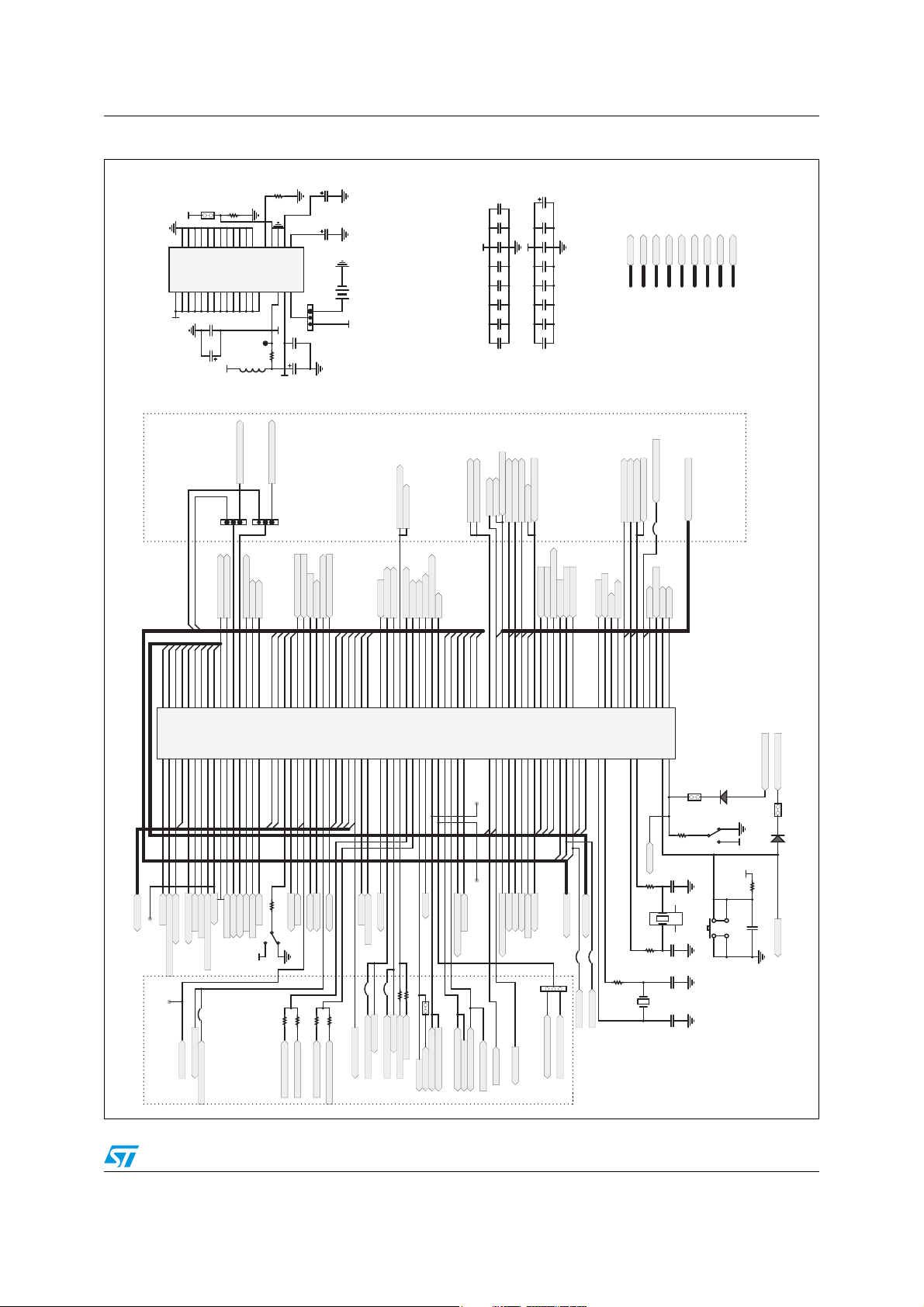
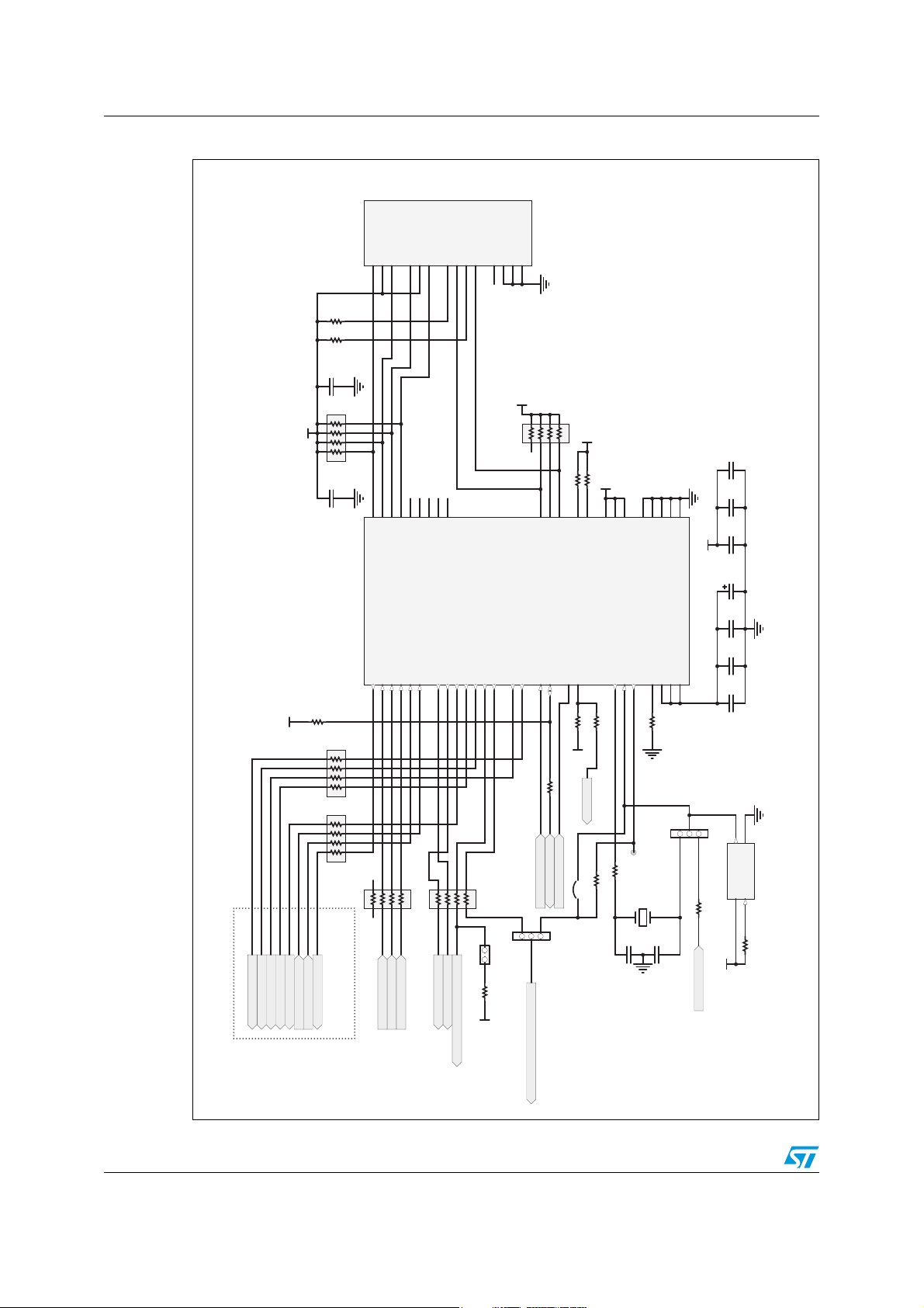
UM1519 Schematics
AM12005v1
ZIGBEE/SPZB32W
PA4
PH13
PC8
Prior to using this adapter, open JP5, JP16, JP21 and JP22,
remove MicroSD card, remove resistors R115 and R140,
disconnect MotorControl board from STM322xG-Eval Board
PH15
PA8
PC9
PC6
PC7
PC11
PC12
PC10
PD2
SC2_SDA
SC2_SCL
GND
nRESET
ZIG_SS
I2C_SDA
VCC-GPIO
ZIG_WAKE
SC1-UART_RXD/SC1-MOSI
JT-TCK
JT-TDO
JT-TDI
JT-TMS
JT-TMS
JT-TDI
JT-TDO
JT-TCK
nRESET
PA6
PA7
ZIG_WAKE
UART_TXD
UART_RXD
PA7
PA6
nRESET
ZIG_MISO
ZIG_HOST_INT
ZIG_MOSI
ZIG_SCLK
E1
GND
I2C_SDA
I2C_SCK
GND
VCC-GPIO
E0
ZIG_SCLK
ZIG_SS
UART_TXD
ZIG_MOSI
UART_RXD
ZIG_MISO
I2C_SCK
I2C_SDA
I2C_SCK
SC1-UART_TXD/SC1-MISO
VCC_3V3
VCC_3V3
VCC_3V3
VCC_3V3
VCC_3V3
VCC_3V3
VCC_3V3
VCC_3V3
VCC_3V3
CN2
Header 20x2 (Female-Bottom)
CN2
Header 20x2 (Female-Bottom)
12
34
5678910
111213
141516
17181920
2122
23
24
2526
2728
293031323334
35
3637383940
J1
Mini-JTAG Conn (10 Pins)
J1
Mini-JTAG Conn (10 Pins)
1 2
3 4
5
678
9 10
CN4
Header 20x2 (Female-Bottom)
CN4
Header 20x2 (Female-Bottom)
1
2
34567
8
91011
12131415161718
1920
21222324
2526
2728
2930
313233
343536
373839
40
R8
470R8470
C1
100nC1100n
1
2
R6
4.7kR64.7k
R12
4.7k
R12
4.7k
D1
LEDD1LED
SW1
RESET
SW1
RESET
R9
470R9470
Antenna
U2
SPW32_MODULE
Antenna
U2
SPW32_MODULE
PA2
10
GND
11
VDD
12
PC1
13
PB0
14
PB115PB2
16
JTCK
17
PC218PC319PC4
20
PC0
21
PB7
22
PA7
25
PC5
26
PA4
3
PA3
4
nRESET
5
PB3
6
PB4
7
PB5
1
PA0
8
PB6
23
PA1
9
PA6
24
PA5
2
R4
10kR410k
JP4
Jumper
JP4
Jumper
2
3
1
R7
4.7kR74.7k
CN3
Header 25x2 (Female-Bottom)
CN3
Header 25x2 (Female-Bottom)
12
3456
7
8
910
11121314
1516
17
18
1920
2122
2324
2526
2728
2930
31
32
3334
3536
3738
3940
4142
4344
4546
4748
4950
R1
4.7kR14.7k
D2
LEDD2LED
JP1
Jumper
JP1
Jumper
2
3
1
JP3
Jumper
JP3
Jumper
2
3
1
R5
4.7kR54.7k
U1
M24LR64U1M24LR64
E0
1
AC0
2
AC1
3
E1
7
SDA
5
SCL
6
VCC
8
VSS
4
R2
4.7kR24.7k
R3
4.7kR34.7k
R11
4.7k
R11
4.7k
C2
100nC2100n
1
2
JP2
Jumper
JP2
Jumper
2
3
1
5 Schematics
Figure 9. ZigBee and dual interface EEPROM adapter for STM322xG-EVAL
Doc ID 022813 Rev 2 27/40
Page 28

Schematics UM1519
AM12006v1
Figure 10. STM3220-21-45-46G-EVAL
28/40 Doc ID 022813 Rev 2
Page 29
UM1519 Schematics
AM12007v1
PA[0..15]
PA[0..15]
PB[0..15]
PB[0..15]
PC[0..15]
PC[0..15]
PD[0..15]
PD[0..15]
PE[0..15]
PE[0..15]
1
4 3
2
B1
RESET
R137
do not t
+3V3
C123
100nF
C73
20pF
C72
20pF
X4
25MHz (with socket)
R86
390
R89
10K
+3V3
2
31
SW2
09.03290.01
RESET#
R88 10K
+3V3
2
3
1
SW1
09.03290.01
41
3
2
X3
MC306
-G-06Q-32.768
(m
anufacturer JF
VNY)
C71
6.8pF
C70
6.8pF
R85
0
R84
0
TP2
PTP_ PPS
Bootloader_BOOT0
Bootloader_RESET
DCMI _PIXCK
DCMI _VSYN
C
DCMI _D[0..7]
DCMI _HSYN C
MCO
ULPI _D[0..7]
ULPI _CL K
ULPI _DIR
ULPI _NXT
ULPI _ST P
RS232/IrDA_TX
RS232/IrDA_RX
OTG_FS_PowerSwitchOn
OTG_FS_OverCurrent
OTG_FS_DM
OTG_FS_D P
OTG_FS_I
D
I2S_WS
I2S_SD
I2S_SCK
I2S_MCK
Audio_DAC_OU
T
CAN1_TX
CAN1_RX
CAN2_T
X
CAN2_RX
MII_TXD0MII_TX_E NMII_TX_CLK
MII_RXD
0
MII_RX_E R
MII_RX_DV/RMII_CRSD
V
MII_RX_CLK/RMII_RE F _CLK
MII_CO
L
MII_CRS
MII_MDC
MII_MDIO
MII_TXD 1
MII_TXD
2
MII_TXD
3
MII_RXD
1
MII_RXD 2
MII_RXD 3
MII_INT
LED4
LED3
LED1
LED2
Potentiometer
Anti_Tam per
WAK E UP
User_Button
I2C1_SCL
I2C1_SDA
IO_Expandor_I
NT
TDI
TRACE_D
3
TRACE_D2
TRACE_D1
TRACE_D0
TRACE_CK
TRS
T
TMS/SWDIO
TCK /SWCLK
TDO/SW
O
D[0..15]
A[0..20]
FSMC_NE3
MicroSDCard_CLK
MicroSDCard_CMD
MicroSDCard_D0
MicroSDCard_D1
MicroSDCard_D2
MicroSDCard_D3
MicroSDCard_Detect
MC_EmergencySTO
P
MC_CurrentA
MC_CurrentB
MC_CurrentC
MC_PFCs ync1
MC_PFCs ync2
MC_W
L
MC_VH
MC_VL
MC_UH
MC_UL
MC_WH
MC_N
TC
MC_Dissipati
veBrake
MC_PFCpwm
MC_EnA
MC_EnB
MC_HeatsinkTem perature
MC_BusVoltage
MC_EnI ndex
SmartCard_3/5V
SmartCard_IO
SmartCard_RST
SmartCard_CL
K
SmartCard_OFF
SmartCard_CMDVCC
FSMC_NE1
FSMC_NE2
FSMC_NWE
FSMC_NO E
FSMC_BL N0
FSMC_BL N1
FSMC_NWAIT
FSMC_CLK
FSMC_NL
OneNAND_INT
PE0
PE1
PE2
PE3
PE4PE5
PE6
PE7
PE8
PE9
PE10
PE11
PE12
PE13
PE14
PE15
PI0
PI1
PI2
PI3
PI4
PI5
PI6
PI7
PI8
PI9
PI 1 0
PI11
PC0
PC1
PC2
PC3
PC4
PC5
PC6
PC7
PC8
PC9
PC1 0
PC11
PC1 2
PC1 3
PC1 4
PC1 5
PF0
PF1
PF2
PF3
PF4
PF5
PF6
PF7
PF8
PF9
PF1 0
PF11
PF12
PF13
PF14
PF15
A0A1A2A3A4
A5
PA0
PA1
PA2
PA3
PA4
PA5
PA6
PA7
PA8
PA1 0
PA 11
PA 1 2
PA 1 3
PA 1 4
PA 1 5
PH0
PH1
PH2
PH3
PH4
PH5
PH6
PH7
PH8
PH9
PH10
PH11
PH12
PH13
PH14
PH15
ULPI _D0
ULPI _D1
ULPI _D2
PB0
PB1
PB2
PB3
PB4
PB5
PB6
PB7
PB8
PB9
PB1 0
PB11
PB1 2
PB1 3
PB1 4
PB1 5
A6
A7
A8
A9
PG0
PG1
PG2
PG3
PG4
PG5
PG6
PG7
PG8
PG9
PG1 0
PG11
PG1 2
PG1 3
PG1 4
PG1 5
A10
A11
ULPI _D3
DCMI _D0
DCMI _D1
DCMI _D2
DCMI _D3
PD0
PD1
PD2
PD3
PD4
PD5
PD6
PD7
PD8
PD9
PD10
PD11
PD12
PD13
PD14
PD15
D13
D14
D15
D4D5D6D7D8
D9
D10
D11
D12
A16
A17
D0
D1
A12
A13
A14
A15
DCMI _D4
D2
D3
DCMI _D5
DCMI _D6
DCMI _D7
DCMI _D[0..7]
A[0..20]
D[0..15]
ULPI _D[0..7]
VBUS_FS
PF[0..15]
PF[0..15]
PG[0..15]
PG[0..15]
PH[0..15]
PH[0..15]
PI[0..11]
PI[0..11]
JP21
BT1
CR1220 holder
L3
BEAD
C74
1uF
C69
100nF
R87
47
VDDA
VDD_MCU
VREF+
C68
100nF
TP5
VREF
1
2
3
JP19
+3V3
VDD_MCU
C60
100nF
VDD_MCU
C50
2.2uF
C33
2.2uF
C48
100nF
C37
100nF
C35
100nF
C54
100nF
C67
100nF
C34
100nF
C57
100nF
VDD_MCU
C56
100nF
C36
100nF
C61
100nF
C66
100nF
C53
100nF
C49
100nF
C65
100nF
IOs MultiplexedIOs Multiplexed
ULPI _D4
ULPI _D5
ULPI _D6
ULPI _D7
R71
10K
C75
1uF
BOOT0
BOOT0
D1
BAT60JFILM
JP29
D2
BAT60JFILM
TP1 4
MCO1
TP1 6
CPU CK
TP1 5
MCO2
A18
A19
A20
Audio_IN
JP34
SB10
SB11
SB12
SB14
SB15
SB16
R34 0
R204
[N/A]
R58 0
R205
[N/A]
123
JP1
123
JP2
PE2A2PE3A1PE4B1PE5B2PE6
B3
PI8
D2
PC1 3
D1
PC1 4E1PC1 5
F1
PI9
D3
PI 1 0E3PI 11
E4
PF0E2PF1H3PF2H2PF3J2PF4
J3
PF5
K3
PF6K2PF7K1PF8L3PF9
L2
PF1 0
L1
PH0
G1
PH1
H1
NRST
J1
PC0
M2
PC1
M3
PC2
M4
PC3
M5
PA0
N3
PA1
N2
PA2
P2
PH2
F4
PH3
G4
PH4
H4
PH5
J4
PA3R2PA4
N4
PA5P4PA6
P3
PA7
R3
PC4N5PC5
P5
PB0R5PB1R4PB2
M6
PF11R6PF1 2P6PF13N6PF1 4R7PF1 5
P7
PG0N7PG1
M7
PE7R8PE8P8PE9
P9
PE10R9PE11
P10
PE12
R10
PE13
N11
PE14
P11
PE15
R11
PB1 0
R12
PB11
R13
PH6
M11
PH7
N12
PH8
M12
PH9
M13
PH10
L13
PH11
L12
PH12
K12
PB1 2
P12
PB1 3
P13
PB1 4
R14
PB1 5
R15
PD8
P15
PD9
P14
PD10
N15
PD11
N14
PD12
N13
PD13
M15
PD14
M14
PD15
L14
PG2
L15
PG3
K15
PG4
K14
PG5
K13
PG6
J15
PG7
J14
PG8
H14
PC6
H15
PC7
G15
PC8
G14
PC9
F14
PA8
F15
PA9
E15
PA1 0
D15
PA 11
C15
PA1 2
B15
PA1 3
A15
PH13
E12
PH14
E13
PH15
D13
PI0
E14
PI1
D14
PI2
C14
PI3
C13
PA1 4
A14
PA 1 5
A13
PC1 0
B14
PC11
B13
PC1 2
A12
PD0
B12
PD1
C12
PD2
D12
PD3
D11
PD4
D10
PD5
C11
PD6
B11
PD7
A11
PG9
C10
PG1 0
B10
PG11B9PG1 2
B8
PG1 3A8PG1 4A7PG1 5
B7
PB3
A10
PB4A9PB5A6PB6B6PB7
B5
BOOT0
D6
PB8
A5
PB9
B4
PE0A4PE1
A3
PI4D4PI5C4PI6C3PI7
C2
U16A
STM32
F207IGH6
VBAT
C1
VSS
F2
VDD
F3
VSS
G2
VDD
G3
VREF-
N1
VSSA
M1
VREF+P1VDDA
R1
BYPASS_RE G
L4
VDD
K4
VSS
M8
VDD
N8
VSS
M9
VDD
N9
VCAP
M10
VDD
N10
VS
S
H12
VDD
J12
VSS_SA
D5
VDD
J13
VSS
G12
VDD
H13
VCAP
F13
VSS
F12
VDD
G13
VSS
D9
VDD
C9
VSS
D8
VDD
C8
VSS
D7
VDD
C7
RFU
C6
VDD_SA
C5
U 1 6 B
STM32F207IFT6
LCD_HSYN
C
LCD_VSYNC
LCD_C
S
R81
10K
JP4
+3V3
1
2
3
JP16
I2S_CKIN
R51 0
R66 [N/A]
C58
4.7uF
STM32F217IGH6
STM32F457IGH6
STM32F467IGH6
Optional
- R F U m e a n s R e s e r v e d f o r Fu t u r e U s e .
- As an option, RFU could be tied to VDD or VSS for forward
compatibility with future STM32F products. However, t he user may leave
R F U pin connected to VDD, or VSS,
or NC for STM32F
ev
is
ulcxe xx2
use.
- J P4 should be tted for future backward compatibilit y with sTM32
F 2 x x .
Figure 11. STM3220-21-45-46G-EVALMCU
Doc ID 022813 Rev 2 29/40
Page 30
Schematics UM1519
MII _TXD0
MII _TX_EN
MII _TX_CLK
MII _RXD0
MII _RX_ER
MII _RX_DV/RMII_CRSD
V
MII _RX_CLK/RMII _RE
F_CL
K
MII _COL
MII _CRS
MII _MDC
MII _MDIO
X1
25MHz
(with socket)
C14
22pF
C15
22pF
123
JP5
MCO
EN
1
GND
2
OUT
3
VCC
4
U3
SM7745HEV-50.0M (do not t)
+3V3
R26
10K
RESET#
R24
0
JP8
R40
2K2
+3V3
+3V3
R25
4.87K
R30 2K2
+3V3
R33 2K2
C21
0.1uF
C17
0.1uF
C19
0.1uF
C13
10uF
R42
2K2
MII _TXD
1
MII _TXD
2
MII _TXD
3
MII _RXD1
MII _RXD
2
MII _RXD3
TX_CLK
1
TX_E
N
2
TXD_03TXD_
1
4
TXD_
2
5
TXD_3/SNI_MODE
6
PWR_DOWN/INT
7
NC8NC9NC
10
NC
11
NC
12
RD -
13
RD+
14
AGND
15
TD-
16
TD+
17
PFBI N 1
18
AGND
19
NC
20
NC
21
AVDD33
22
PFBOU T
23
RB
IAS
24
25MHz_OUT
25
LED_ACT/COL/AN_EN
26
LED_SPEED/AN1
27
LED_LIN K/AN0
28
RESET_N
29
MDIO30MDC
31
IOVDD33
32
X233X1
34
IOGND
35
DGND
36
PFBI N 2
37
RX_CLK
38
RX_DV/MII _MODE
39
CRS/CRS_DV/L
ED_CF
G
40
RX_ER/MDIX_E N
41
COL / PHYAD0
42
RXD_0/P HYAD143RXD_1/
PHYAD2
44
RXD_2/
PHYAD3
45
RXD_3/P HYAD4
46
IOGND
47
IOVDD33
48
U5
DP83848CVV
+3V3
C16
0.1uF
C27
0.1uF
C20
0.1uF
+3V3
R43
1.5K
1
2
3
JP6
TP1
25MHz
TD+
1
TCT
4
TD-
2
RD+3RCT
5
RD -
6
NC
7
CHS GND
8
LED(green)_A
9
LED(green)_
K
10
LED(Yellow)_A
12
LED(Yellow)_K
11
Shield
13
Shield
14
CN7
J0011D21B
R22
240
R1
240
+3V3
C7
0.1uF
C6
0.1uF
+3V3
MII _INT
R41 0
R44 0 Second
source: SI-60116- F
RS5
51
RS3
51
RS6
51
+3V3
Unused in RMII mode
RS1
2K2
RS4
51
RS2
51
PI1 0
PC1
PC2
PC3
PA 1
PA 2
PH2
PH3
PA 7
PC4
PC5
PG11
PH6
PH7
PG13
PG14
PB1 4
PB8
PA 8
SB1
R208
51
R212
150
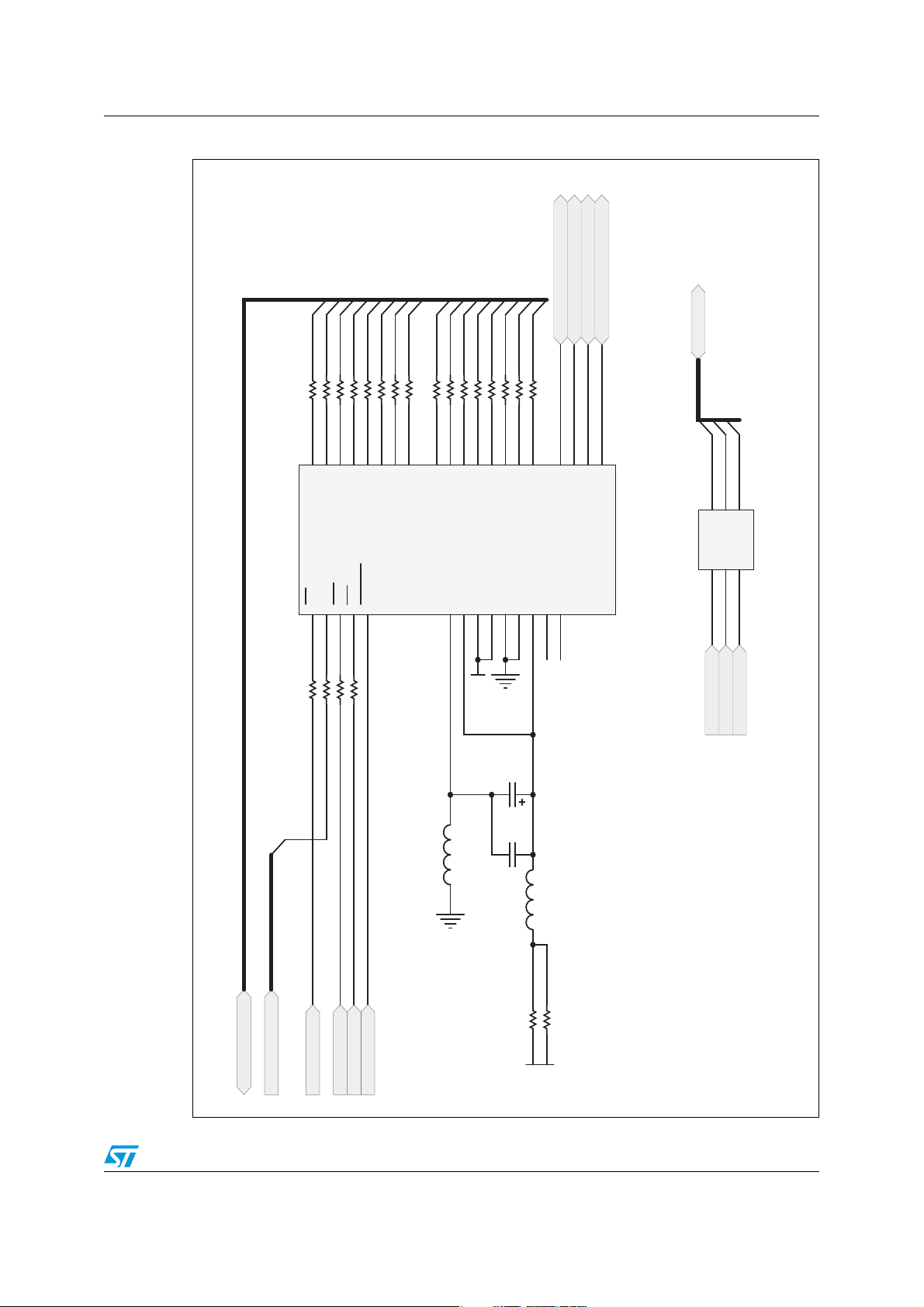
AM12008v1
Figure 12. STM3220-21-45-46G-EVALEthernet
30/40 Doc ID 022813 Rev 2
Page 31
UM1519 Schematics
TouchScreen_X+
TouchScreen_X-
TouchScreen_Y+
TouchScreen_Y-
CS
1
RS
2
WR/SCL
3
RD
4
RESET
5
VDD24VCI25GND26GND27BL _VDD
28
BL _Control
23
BL _GND
22
PD1
6
PD2
7
PD3
8
PD4
9
PD5
10
PD611PD712PD8
13
PD 10
14
PD 11
15
PD 12
16
PD 13
17
PD 1418PD 1519PD 1620PD 17
21
SDO
29
SDI
30
XL
31
XR
32
YD
33
YU
34
CN19
3.2" LCD_connector (MB785 with AM-240320D4TOQW-T00H(R))
+3V3
+5 V
To I/O expandor
RESET#
D[0..15]
A[0..20]
A[0..20]
D[0..15]
FSMC_NWE
FSM C_NO E
FSMC_NE3
D0
D1
D2D3D4
D5D6D7
D8
D9
D10
D11
D12
D13
D14
D15
A0
PD5
PD4
PG10
R170 150
R171 150
R172 150
R173 150
R174 150
R175 150
R176 150
R177 150
R82 150
R161 150
R163 150
R165 150
R166 150
R167 150
R168 150
R169 150
R78 150
R119 150
R162 150
R164 150
C148
10uF
L2
BEAD
C153
100nF
L1
BEAD
LCD_HSYNC
LCD_VSYN C
LCD_C S
1
2
3 4
5 6
CN22
Header 3X2H
PC[0..15]
PC 10
PC 11
PC 12
PC[0..15]
Reserved
for LCD
connector
R67 0
+3V3
R68 [N/A]
AM12009v1
Figure 13. STM3220-21-45-46G-EVALLCD
Doc ID 022813 Rev 2 31/40
Page 32

Schematics UM1519
AM12004v1
Enable
DotClk
HSYNC
VSYNC
CSRSWR
RD
#RESET
SDO
SDI
VDD
PD0
PD1
PD2
PD3
PD4
PD5
PD6
PD7
PD8
PD9
PD1 0
PD1 1
PD1 2
PD1 3
PD1 4
PD1 5
PD1 6
PD1 7
YUYDXR
XL
VSS
1
XL
2
XR
3
YD4YU
5
VSS
6
IM0/ID
7
IM18IM3
9
SDO
10
NC
11
SDI
12
D1713D1614D1515D1416D1317D1218D1119D10
20
D921D822D723D624D525D426D327D228D129D0
30
CS
31
RESET
32
RS33WR/SCL34RD
35
VSYNC36HSYNC37DOTCLK38ENABLE
39
VCC40VCC
41
VSS
42
LED_K
43
LED_A
44
VSS
45
CN2
FF0245SS1
R4
0
R1
10K
VDD
RP1
10K
RP2
10K
RP4
10K
PD0
PD2
PD4
PD6
PD8
PD9
PD10
PD11
PD12
PD1 3
PD14
PD15
PD16
PD17
Enable
DotClk
HSYNC
VSYNC
VDD
C3
1uF/50V
R3
4K7R24K7
SDI
SDO
RD
RS
Soldered for Serial interface only
Soldered for i80-system 16-bit interface
The 34-pin connector to motherboard for both
serial & 16bit interface. Compatible with
MB694 with touchscreen signals added on
Pin 31-34.
CSRSWRRD#RESET
VDD
BLGND
BLVDD
BL_Control
PD1
PD2
PD3
PD4
PD5
PD6
PD7
PD8
PD1 0
PD1 1
PD1 2
PD1 3
PD1 4
PD1 5
PD1 6
PD1 7
SDO
SDI
A
K
Z1
STPS1L40M
C1
4.7uF/50V
L1
4.7uH(1A)
R7
10
BLGND
BLVDD
R6
100K
C2
2.2uF
R5
0
R8
do not fit
BLVDD
BL_Control
BLGND
BLGND
BLGND
AM-240320D4TOQW-T00H(R)
Vi
1
Rset
2
GND
3
FB
4
NC
5
Vo
6
EN
7
SW
8
PGN D
9
U1
STLD40DPMR
CS1RS2WR/SCL3RD4RESET
5
VDD24VCI25GND26GND27BL_VDD
28
BL_Control
23
BL_GND
22
PD16PD27PD38PD49PD510PD611PD712PD8
13
PD1 014PD1 115PD1 216PD1 317PD1 418PD1 519PD1 620PD1 7
21
SDO29SDI
30
XL
31
XR
32
YD33YU
34
CN1
3.2LCD_connector
YU
YD
XR
XL
LCD board connector to motherboard
RP3
10K
RP6
10K
RP5
10K
PD1
PD3
PD5
PD7
Figure 14. LCD module with both SPI and 16-bit interface
32/40 Doc ID 022813 Rev 2
Page 33

AM12010v1
R 1 4 7
10K
R 1 4 6
10K
R 1 4 5
10K
R 1 4 4
10K
R 1 4 9
10K
+2V8
C119 100nF
C12 8 10 0 n F
C12 0 10 0 n F
C12 9 10 0 n F
C12 1 10 0 n F
R159
100
COMMON
5
Selection
2
DWON
3
LEFT
1
RIGHT
4
UP
6
U32
MT008-A
JOY_SEL
JOY_DOWN
JOY_LEF T
JOY_RIGHT
JOY_UP
To IO expandor
EEP ROM_SCL
EEP ROM_SDA
E0
1
E1
2
E2
3
VSS4SDA
5
SCL
6
WC
7
8
U18
M24C64-RMN6T P
+3V3
R102
10K
JP2 4
C81
100nF
PB9
PB6
R153
220K
1
4
3
2
B2
WK U P
C124
do not t
+3V3
R138
100
R148
4K7
1
4
3
2
B4
USER
C130
100nF
+3V3
R160
100
R142
4K7
1
4 3
2
B3
Tamper
C118
100nF
+3V3
R156
100
R139
330
R150
0
R143
0
Anti_Tamper
WAKEUP
User_Button
PC1 3
PA0
PG1 5
3
1
2 RV1
3386P-103H[10%]
R151
0
+3V3
Potentiometer
C122
10nF
R152
1K
PF9
1 2
LD3
Red
1 2
LD2
Orange
1 2
LD4
Blue
1 2
LD1
Green
R155
510
R154
680
R141
680
R140
680
LED4
LED3
LED1
LED2
PG6
PG8
PI9
PC7
MEMS_SCL
MEMS_SDA
MEMS_I NT1
MEMS_I NT2
VDD_IO
1
GND
2
Reserved
3
GND
4
GND
5
VDD
6
CS
7
INT1
8
INT2
9
GND
10
Reserved
11
SDO
12
SDA
13
SCL
14
U20
LIS302D L
+2V8
R107
10 K
+2V8
C89
100nF
To IO expandor
PB9
PB6
VCC
UM1519 Schematics
Figure 15. STM3220-21-45-46G-EVAL I/O peripherals
Doc ID 022813 Rev 2 33/40
Page 34

Schematics UM1519
AM12011v1
Y-
1
INT
2
A0/Data Out
3
SCLK
4
SDAT
5
VCC
6
Data in
7
IN0
8
IN1
9
GND
10
IN2
11
IN3
12
X+
13
Vio
14
Y+
15
X-
16
U24
STMP E811QTR
Y-
1
INT
2
A0/Data Out
3
SCLK
4
SDAT
5
VCC
6
Data in
7
IN0
8
IN 1
9
GND
10
IN2
11
IN3
12
X+
13
Vio
14
Y+
15
X-
16
U29
STMPE811QTR
R135
10K
+2V8
I2C device address:0x82
I2C dev ice address:0x88
+2V8
+2V8
R116
100K
R132
100K
IO_Expandor_SCK
IO_Expandor_SDA
IO_Expandor_INT
TouchScreen_X+
TouchScreen_XTouchScreen_Y+
TouchScreen_Y-
EXP _IO2
EXP _IO3
EXP _IO4
EXP _IO5
EXP _IO6
EXP _IO7
EXP _IO8
EXP _IO 9
EXP _IO10
EXP _IO11
EXP _IO12
EXP _IO1
R121
10K
R136 0
+2V8
R117
10K
R131
10K
+2V8
C99
100nF
C115
100nF
PB 9
PB 6
PI2
Figure 16. STM3220-21-45-46G-EVAL I/O_Expander
34/40 Doc ID 022813 Rev 2
Page 35

UM1519 Schematics
AM12012v1
1
2345678910
11121314151617
18
19
20
R97
[N/A]
[N/A]
R101
[N/A]
R95
[N/A]
R9 8
do not t
1
2
3
4
567
8
9
10
11
12
13
14
15
16
17
18
19
20
+3V3
+3V3
R105 10 K
R106 10 K
R99
10K
R92
[N/A]
R 1040
R 100 do not t
R 9
do not t
TRACE_D 3
TRACE_D 2
TRACE_D 1
TRACE_D 0
TRACE_CK
PE 6
PE 5
PE 4
PE 3
PE 2
TDI
RESET#
TRST
TMS/SWDIO
TC
K /SWCL K
TD O/ S W O
D8
Z5V1
RS7
22
Z5V1
D4
Z5V1
Z5V1
D6
Z5V1
D7
Z5V1
0
R96
+3V3
PA13
R91
PB3
PA15
PA14
PB4
+3V3
D3
D5
Figure 17. STM3220-21-45-46G-EVAL JTAG and trace
Doc ID 022813 Rev 2 35/40
Page 36

AM12013v1
Vin
3
GND
1
Vout
2
U22
LD1086D2M33TR
C113
220uF
C83
10uF
C82
100nF
+5V
3V3
+3V3
Vin3Vout
2
1
U21
LD1117S25T R
+5V
C91
10uF
+2V 5
TP 6
2V 5
C96
220uF
Vin3Vou t
2
1
U30
LD1117S18T R
C116
10uF
+1V8
1V8
+3V3 VDD_ MCU
JP32
SV
1
SG
2
CV
3
CG 1
4
CG 2
5
CG 3
6
U25
BNX002-01
C106
10uF
E5 V
1
3
2
CN18
DC- 10 B
Z1
SMAJ5.0A-T R
C112
100nF
1
2
3
U28
ZEN056V130A24LS
TP 8
5V
+5V
R93
1K
1
2
LD9
red
TP 1 3
Ground
D5V
E5V
VBUS_FS
VBUS_H S
Vin3Vout
2
1
U26
LD1117STR
+5V
C110
10u F
+2V8
TP 9
2V 8
R114
120
C100
10uF
R120
150
1 2
3 4
5 6
7 8
9 10
JP18
Header 5X2
U5V_ST_LIN K
Schematics UM1519
Figure 18. STM3220-21-45-46G-EVALPower
36/40 Doc ID 022813 Rev 2
Page 37

UM1519 Schematics
AM12014v1
RESET#
RESET#
12
34
56
789
10
1112
1314
1516
17
18
1920
21222324
25
26
27
28
29
30
3132
3334
3536
37
38
3940
21N22564
-
40S10B
1 2
3 4
5 6
7 8
9 10
11 12
13 14
15 16
17 18
19 20
21 22
23 24
25 26
27
28
29 30
31
32
33 34
35 36
37 38
39 40
41
42
43 44
45 46
47 48
49 50
CN1
21N22564 -50S10B
12
3
4
5
6
7
8
910
1112
1314
1516
1718
1920
2122
2324
2526
2728
29
303132
3334
3536
3738
3940
21N22564-40S10B
1
2
3 4
5 6
7 8
9 10
11
12
13 14
15
16
17 18
19 20
21 22
23 24
25 26
27 28
29 30
31 32
33 34
35 36
37
38
39 40
41
42
43 44
45
46
47 48
49
50
CN3
21N22564- 50S10B
1AP0AP
PA 2
P A 3P A 4
P A 5P A 6
P A 7
P A8
P A1 0P A1 1
PA 1 2
P A1 3
P A14 P A15
P B 0
P B 1
P B 2
PB3 P B 4
PB5 P B 6
PB7
P B 8
P B 9
P B10
P B11
PB1 2P B1 3
PB1 4
P B1 5
PC0
2CP1CP
PC3
P C 4
P C 5
PC 6
P C 7
P C 8P C 9
P C10 P C11
P C12
PC13
EXT _ PC1 4
EXT _ PC1 5
PD0
P D1 P D 2
P D3
P D4 P D 5
P D6 P D 7
P D8
P D9P D1 0
P D1 1P D1 2
P D1 3P D1 4
P D1 5
P E 0
P E 1
P E 2
4EP3EP
6EP5EP
P E 7
P E 8P E 9
P E10P E11
P E12P E 13
P E14
P E15
1FP0FP
3FP2FP
PF4
PF6
PF8
01FP9FP
P F1 1
P F1 2
P F1 3
P F1 4P F15
PG 0
P G1
P G 2P G 3
P G 4P G 5
P G 6P G 7
P G 8
P G9 P G10
P G11 P G12
P G13
P G14 P G 1 5
EXT _ P H 0 EX T _ P H 1
P H2
P H3
5HP4HP
P H6
P H 7
P H8
P H 9P H10
P H11
P H1 2
P H1 3
P H1 4P H1 5
P I0PI1
P I2
PI3
P I 4
6I P5IP
P I7
PI8
P I9
11IP01IP
VREF+
EMU_3V3
EMU_5 V
APP_3V3
APP_VCC
P C13
R E S E T #
EMU_5V
EMU_3V3
EMU_5 V
APP_3V3
BOOT
0
(Left)
(Bottom) (Top)
PA[0..15]
PA[0..15]
PB[0..15]
PB[0..15]
PC[0..15]
PC[0..15]
PD[0..15]
PD[0..15]
PE[0..15]
PE[0..15]
PF[0..15]
PF[ 0 .. 1 5 ]
PG[0..15]
PG[0..15]
PH[0..15]
PH[0..15]
PI[0..11]
PI[ 0. .1 1 ]
APP_3V3
APP_VCC
EMU_5V
D5V
+3V3
SB6
SB7
SB4
SB5
PH0
PH1
PC 14
PC 15
EXT_P H0
EXT_P H1
EXT_
P C14
EXT_
P C15
Close to
crystal
on
PCB
BOOT0
BOOT0
VBUS_FS
PF5
PF7
CN4
CN2
(Right)
Figure 19. STM3220-21-45-46G-EVALExtension connector
Doc ID 022813 Rev 2 37/40
Page 38

References UM1519
6 References
1. AN4139, application note
2. STEVAL-IHP004V1 schematics diagram
3. M24LR64-r - datasheet
4. SPZB32W1A2.1 Module - datasheet
38/40 Doc ID 022813 Rev 2
Page 39

UM1519 Revision history
7 Revision history
Table 14. Document revision history
Date Revision Changes
09-Jul-2012 1 Initial release.
27-Sep-2012 2 Modified: Figure 3
Doc ID 022813 Rev 2 39/40
Page 40

UM1519
Please Read Carefully:
Information in this document is provided solely in connection with ST products. STMicroelectronics NV and its subsidiaries (“ST”) reserve the
right to make changes, corrections, modifications or improvements, to this document, and the products and services described herein at any
time, without notice.
All ST products are sold pursuant to ST’s terms and conditions of sale.
Purchasers are solely responsible for the choice, selection and use of the ST products and services described herein, and ST assumes no
liability whatsoever relating to the choice, selection or use of the ST products and services described herein.
No license, express or implied, by estoppel or otherwise, to any intellectual property rights is granted under this document. If any part of this
document refers to any third party products or services it shall not be deemed a license grant by ST for the use of such third party products
or services, or any intellectual property contained therein or considered as a warranty covering the use in any manner whatsoever of such
third party products or services or any intellectual property contained therein.
UNLESS OTHERWISE SET FORTH IN ST’S TERMS AND CONDITIONS OF SALE ST DISCLAIMS ANY EXPRESS OR IMPLIED
WARRANTY WITH RESPECT TO THE USE AND/OR SALE OF ST PRODUCTS INCLUDING WITHOUT LIMITATION IMPLIED
WARRANTIES OF MERCHANTABILITY, FITNESS FOR A PARTICULAR PURPOSE (AND THEIR EQUIVALENTS UNDER THE LAWS
OF ANY JURISDICTION), OR INFRINGEMENT OF ANY PATENT, COPYRIGHT OR OTHER INTELLECTUAL PROPERTY RIGHT.
UNLESS EXPRESSLY APPROVED IN WRITING BY TWO AUTHORIZED ST REPRESENTATIVES, ST PRODUCTS ARE NOT
RECOMMENDED, AUTHORIZED OR WARRANTED FOR USE IN MILITARY, AIR CRAFT, SPACE, LIFE SAVING, OR LIFE SUSTAINING
APPLICATIONS, NOR IN PRODUCTS OR SYSTEMS WHERE FAILURE OR MALFUNCTION MAY RESULT IN PERSONAL INJURY,
DEATH, OR SEVERE PROPERTY OR ENVIRONMENTAL DAMAGE. ST PRODUCTS WHICH ARE NOT SPECIFIED AS "AUTOMOTIVE
GRADE" MAY ONLY BE USED IN AUTOMOTIVE APPLICATIONS AT USER’S OWN RISK.
Resale of ST products with provisions different from the statements and/or technical features set forth in this document shall immediately void
any warranty granted by ST for the ST product or service described herein and shall not create or extend in any manner whatsoever, any
liability of ST.
ST and the ST logo are trademarks or registered trademarks of ST in various countries.
Information in this document supersedes and replaces all information previously supplied.
The ST logo is a registered trademark of STMicroelectronics. All other names are the property of their respective owners.
© 2012 STMicroelectronics - All rights reserved
STMicroelectronics group of companies
Australia - Belgium - Brazil - Canada - China - Czech Republic - Finland - France - Germany - Hong Kong - India - Israel - Italy - Japan -
Malaysia - Malta - Morocco - Philippines - Singapore - Spain - Sweden - Switzerland - United Kingdom - United States of America
www.st.com
40/40 Doc ID 022813 Rev 2
 Loading...