

查询Z01xxxN供应商
FEATURES
I
V
I
=1A
T(RMS)
=400V to 800V
DRM
≤ 3mAto ≤ 25mA
GT
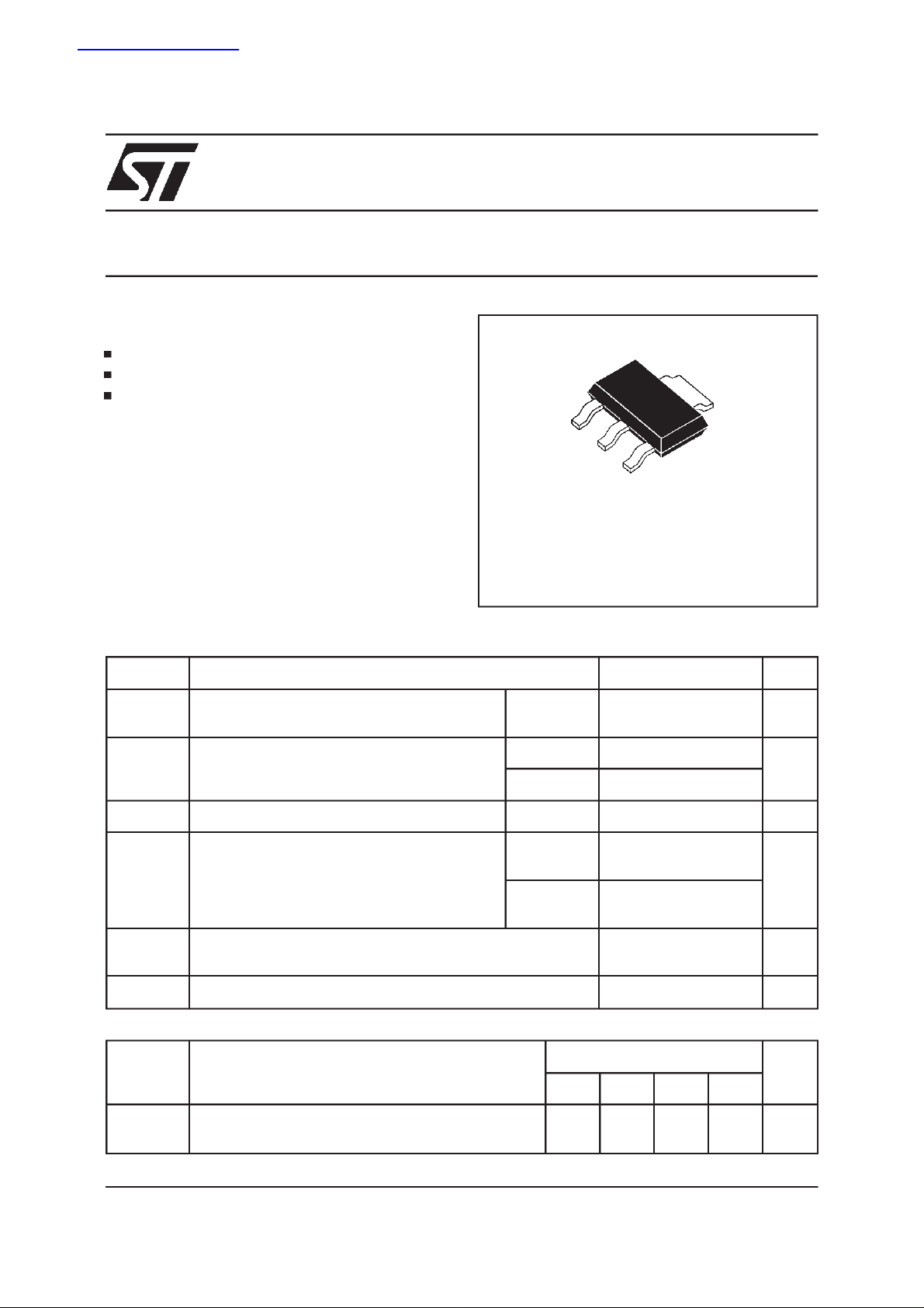
DESCRIPTION
The Z01xxxN series of triacs uses a high
performance TOP GLASS PNPN technology.
These parts are intended for general purpose
high volume applications using surface mount
technology.
ABSOLUTE RATINGS
(limitingvalues)
Z01xxxN
SENSITIVEGATE TRIACS
A2
A1
A2
G
SOT223
(Plastic)
Symbol Parameter Value Unit
I
T(RMS)
RMSon-statecurrent
Ttab=90 °C1 A
(360°conductionangle)
I
TSM
Nonrepetitivesurge peak on-statecurrent
(T
initial= 25°C)
j
tp = 8.3 ms 8.5 A
tp = 10 ms 8
2
tI
I
dI/dt Criticalrateof riseofon-statecurrent
2
t Valuefor fusing tp = 10 ms 0.35 A2s
=50mA diG/dt= 0.1 A/µs.
I
G
Repetitive
F = 50 Hz
Non
10 A/µs
50
Repetitive
T
stg
T
j
Storageand operating junctiontemperature range
-40, + 150
-40, + 125
°
C
Tl Maximumlead temperatureforsolderingduring 10s 260 °C
Voltage
Symbol Parameter
Unit
DMSN
V
DRM
V
RRM
Repetitivepeak off-statevoltage
T
= 125°C
j
400 600 700 800 V
May 1998 Ed: 1A
1/6
Z01xxxN
THERMALRESISTANCES
Symbol Parameter Value Unit
Rth(j-a) Junctionto ambient 60
Rth(j-t) Junctionto leadsfor D.C 30 °C/W
Rth(j-t)
GATECHARACTERISTICS
P
= 0.1W PGM= 2 W (tp = 20 µs) IGM= 1 A (tp =20 µs)
G (AV)
Junctionto leadsfor A.C 360°conductionangle (F=50Hz)
(maximumvalues)
25
ELECTRICAL CHARACTERISTICS
Symbol TestConditions
Quadrant
Sensitivity
03 07 09 10
I
GT
VD=12V (DC) RL=140Ω Tj= 25°C I-II-III MAX 3 5 10 25 mA
IV MAX 5 7 10 25
V
GT
V
GD
tgt V
VD=12V (DC) RL=140Ω
VD=V
DRMRL
D=VDRMIG
I
=1.4A
T
dI
/dt = 0.5A/µs
G
Ω
=3.3k
=40mA
Tj=25°C I-II-III-IV MAX 1.5 V
Tj=125°C I-II-III-IV MIN 0.2 V
Tj=25°C I-II-III-IV TYP 2 µs
°
C/W
°
C/W
Unit
I
*I
H
I
L
*ITM= 1.4A tp=380µs Tj=25°C MAX 1.8 V
V
TM
I
DRM
I
RRM
dV/dt* VD=67%V
(dV/dt)c*
= 50 mA Gateopen Tj=25°C MAX7 101025 mA
T
IG=1.2 I
VD=V
VR=V
GT
DRM
RRM
Gateopen Tj=110°C MIN 10 20 50 100 V/µs
DRM
(dI/dt)c= 0.44A/ms
* For either polarityof electrodeA
ORDERINGINFORMATION
Z0107MN
TRIACTOP GLASS
Tj=25°C I-III-IV TYP 7 10 10 25 mA
II TYP 14 20 20 50
Tj=25°C MAX 10 µA
Tj=110°C MAX 200
Tj=110°C MIN 2 5 V/µs
voltagewith referenceto electrodeA
2
TYP 1 1
1
PACKAGE:
N = SOT223
2/6
CURRENT
SENSITIVITY
VOLTAGE

Z01xxxN
Fig.1 :
Maximum power dissipation versus RMS
on-statecurrent.
P(W)
1.6
1.4
1.2
1.0
0.8
0.6
0.4
0.2
0.0
0.0 0.1 0.2 0.3 0.4 0.5 0.6 0.7 0.8 0.9 1.0
Fig.3 :
RMS on-state current versus tab tempera-
180
=30
O
=60
o
=90
o
=120
o
= 180
o
o
I(A)
T(RMS)
ture.
I (A)
T(RMS)
1.2
Fig.2:
Correlationbetweenmaximumpowerdissipation and maximum allowable temperature
(Tamband Ttab).
o
P(W)
Ttab ( C)
1.6
1.4
1.2
1.0
o
Rth(j-a) C/W
o
Rth(j-t) C/W
0.8
0.6
0.4
0.2
0.0
0 20406080100120140
Fig.4 :
o
Tamb ( C)
Relative variation of thermal impedance
-90
-95
-100
-105
-110
-115
-120
-125
junctionto ambient versus pulseduration.
Zth(j-a)/Rth(j-a)
1.00
1.0
0.8
=180
o
0.6
0.4
0.2
0
0 102030405060708090100110120130
o
Ttab( C)
Fig.5: Relativevariationof gatetriggercurrentand
holdingcurrentversusjunction temperature.
Igt[Tj]
Igt[Tj=25 C]
2.6
2.4
2.2
2.0
1.8
1.6
1.4
Ih
1.2
1.0
0.8
0.6
0.4
-40 -20 0 20 40 60 80 100 120 140
o
Igt
Tj( C)
Ih[Tj]
Ih[Tj=25 C]
o
o
0.10
Standard foot print , e(Cu) =35
0.01
1E-3 1E-2 1E-1 1 E+0 1E+1 1E+2 5E+2
m
tp(s)
Fig.6 : Non repetitive surge peak on-state current
versusnumberof cycles.
I (A)
TSM
8
6
4
2
Number of cycles
0
1101001000
Tj initial = 25 C
o
3/6

Z01xxxN
Fig.7:
for a sinusoidal pulsewith width : tp ≤ 10ms, and
correspondingvalueofI
100
Nonrepetitivesurge peakon-state current
2
t.
I (A). I2t(A2s)
TSM
Tj initial = 25 C
I
TSM
o
Fig.8:
I (A)
TM
10
On-statecharacteristics(maximumvalues).
Tj initial
o
25 C
10
1
Tj max
1
I2t
tp(ms)
0.1
110
0.1
00.511.522.533.544.55
Tj max
Vto =1.10 V
Rt =0.420
V (V)
TM
4/6

PACKAGEMECHANICAL DATA
SOT223(Plastic)
A
A1
H
E
B1
e1
D
B
e
t
V
S
Z01xxxN
DIMENSIONS
REF.
V1
A1
V2
A 1.50 1.70 0.059 0.067
A1 0.02 0.10 0.001 0.004
C
B 2.95 3.15 0.090 0.124
B1 0.65 0.85 0.026 0.033
O
C 0.25 0.35 0.010 0.014
D 6.30 6.70 0.248 0.264
e 2.3 0.091
e1 4.6 0.181
E 3.30 3.70 0.130 0.146
H 6.70 7.30 0.264 0.287
O 0.63 0.65 0.67 0.025 0.026 0.026
S 0.85 1.05 0.033 0.041
t 1.10 1.30 0.043 0.051
V10°max
V1 10°min 16°max
V2 10°min 16°max
Millimeters Inches
Min. Typ. Max. Min. Typ. Max.
Weight: 0.11 g
FOOTPRINT
5/6

Z01xxxN
MARKING
Z0103DN Z3D
Z0103MN Z3M
Z0103SN Z3S
Z0103NN Z3N
Z0107DN Z7D
Z0107MN Z7M
Z0107SN Z7S
Z0107NN Z7N
Z0109DN Z9D
Z0109MN Z9M
Z0109SN Z9S
Z0109NN Z9N
Z0110DN Z0D
Z0110MN Z0M
Z0110SN Z0S
Z0110NN Z0N
Type Marking
Informationfurnished is believed tobeaccurate and reliable. However, STMicroelectronicsassumes no responsibility for theconsequences of
use of such information nor for any infringementof patents or otherrights ofthird parties which may resultfrom its use. No license isgranted by
implication or otherwise under any patent or patent rights of STMicroelectronics. Specificationsmentioned in this publication are subject to
change without notice. This publicationsupersedes and replaces all information previously supplied.
STMicroelectronics products are not authorized for use as critical components in life support devices or systems withoutexpress written approval of STMicroelectronics.
1998 STMicroelectronics - Printed inItaly - All rights reserved.
STMicroelectronics GROUP OF COMPANIES
Australia- Brazil -Canada - China- France-Germany- Italy-Japan -Korea- Malaysia -Malta- Mexico- Morocco- The
Netherlands -Singapore - Spain-Sweden- Switzerland- Taiwan -Thailand - United Kingdom- U.S.A.
6/6
 Loading...