

Page 1
UM2641
User manual
Getting started with the X-NUCLEO-S2915A1 Sub-1 GHz 915 MHz RF expansion
board based on S2-LP radio for STM32 Nucleo
Introduction
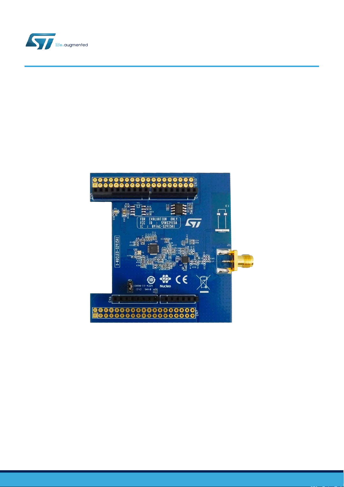
The X-NUCLEO-S2915A1 expansion board is based on the S2-LP radio and operates in the 915 MHz ISM frequency band.
The expansion board is compatible with ST morpho and Arduino UNO R3 connectors.
The X-NUCLEO-S2915A1 interfaces with the STM32 Nucleo microcontroller via SPI connections and GPIO pins. Y
change some of the GPIOs by mounting or removing the resistors.
Figure 1. X-NUCLEO-S2915A1 expansion board
ou can
UM2641 - Rev 1 - November 2019
For further information contact your local STMicroelectronics sales of
fice.
www.st.com
Page 2
1 Acronyms and abbreviations
Table 1. List of acronyms
Acronym Description
AMR Automatic meter reading
EEPROM Electrically erasable programmable read only memory
GHz Giga Hertz
GUI Graphical user interface
LED Light emitting diode
MCU Microcontroller unit
P2P Point-to-point communication
RF Radio frequency communication
SPI Serial peripheral interface
USB Universal serial bus
wM-Bus Wireless metering bus
WSN Wireless sensors network
UM2641
Acronyms and abbreviations
UM2641 - Rev 1
page 2/20
Page 3

2 Getting started
2.1 Overview
The X-NUCLEO-S2915A1 main features are:
Based on S2-LP radio
•
• S2-LP narrow band ultra-low power sub-1 GHz transceiver tuned for 860-940 MHz frequency band
• Programmable RF output power up to +27 dBm
• Modulation schemes: 2-FSK, 2-GFSK, 4-FSK, 4-GFSK, OOK and ASK
• Air data rate from 0.1 to 500 kbps
• Ultra-low power consumption: 7 mA RX and 10 mA TX at +10 dBm
• IEEE 802.15.4g hardware packet support with whitening, FEC, CRC and dual SYNC word detection
• RX and TX 128 byte FIFO buffers
• Support to wireless M-Bus
• Excellent performance of receiver sensitivity (up to -130 dBm)
• Automatic acknowledgement, retransmission and timeout protocol engine
• Compatible with STM32 Nucleo boards
• Compatible with Arduino UNO R3 connectors
• Sigfox compatible
• Sample firmware for P2P communication
• 6LoWPAN compatible thanks to STM32Cube
• FCC ID: S9NS2915A
• IC ID: 8976C-S2915A1
• RoHS and WEEE compliant
UM2641
Getting started
2.2 Typical applications
The X-NUCLEO-S2915A1 expansion board can be used for the evaluation of the S2-LP device in multiple
applications:
•
wM-Bus application
• Point-to-point communication protocol
• 6LoWPAN applications
• SigFox communication
You can develop other applications for evaluating the devices, such as:
• Automatic meter reading
• Home and building automation
• WSN
• Industrial monitoring and control
• Wireless fire and security alarm systems
UM2641 - Rev 1
page 3/20
Page 4
2.3 Hardware and software requirements
UM2641
Hardware and software requirements
To use STM32 Nucleo development boards with the X-NUCLEO-S2915A1
as shown below.
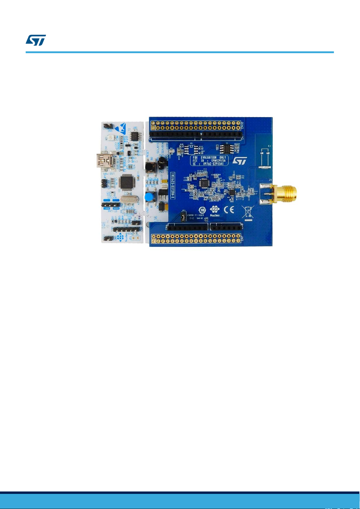
Figure 2. X-NUCLEO-S2915A1 expansion board connected to an STM32 Nucleo development board
expansion board, connect the boards
The interconnection between the STM32 Nucleo and the X-NUCLEO-S2915A1 has been designed to allow using
any STM32 Nucleo board, although complete testing has been performed using NUCLEO-L053R8, NUCLEO-
F401RE and NUCLEO-L152RE boards hosting the ultra-low power STM32.
The following software and hardware specifications are required:
• a PC/laptop with Microsoft Windows (7 and above) to install the software package (X-CUBE-SUBG1)
• a type A USB to mini-B USB cable to connect the STM32 Nucleo board to the PC/laptop
• 128 MB of RAM
• Approximately 40 MB of hard disk space for the firmware
• Approximately 15 MB of hard disk space for the wM-Bus GUI
The use of the wM-Bus concentrator with the GUI requires additional boards to be connected to the PC. The GUI
can be used to check the wM-Bus communication protocol.
2.4 Board setup
Step 1. Check that the jumper on JP1 connector is connected to provide the required voltage to the board
devices.
Step 2. Connect the X-NUCLEO-S2915A1 to the STM32 Nucleo
Step 3. Power the Nucleo development board using the Mini-B USB cable.
Step 4. Program the firmware in the STM32 on the Nucleo development board using the firmware sample
provided.
Step 5. Reset the MCU board using the reset button on the Nucleo development board.
The evaluation kit is ready-to-use.
board.
UM2641 - Rev 1
page 4/20
Page 5
Hardware description and configuration
3 Hardware description and configuration
3.1 Interconnection details
The X-NUCLEO-S2915A1 expansion board and the NUCLEO-F401RE or NUCLEO-L152RE board connection
details are listed in the table below
Table 2. X-NUCLEO-S2915A1 and NUCLEO-L152RE connection details (left connector)
NC IOREF RESET 3V3
CN6 Power CN8 Analog
1 2 3 4 5 6 7 8 1 2 3 4 5 6
3V3 GND GND GPIO0 CSN GPIO1 GPIO2
5
.
Signal name
V
GND GND VIN A0 A1 A2 A3 A4 A5
Connector name
Pin number
NUCLEO-L152RE MCU port
PA0 PA1 PA4 PB0 PC1 PC0
X-NUCLEO-S2915A1 expansion board signals
GPIO0
UM2641
(1)
GPIO3
Optional connection.
1.
Table 3. X-NUCLEO-S2915A1 and NUCLEO-L152RE connection details (right connector)
Signal name
D15 D14 AREF GND D13 D12 D11 D10 D9 D8 D7 D6 D5 D4 D3 D2 D1 D0
Connector name
CN5 Digital CN9 Digital
Pin number
10 9 8 7 6 5 4 3 2 1 8 7 6 5 4 3 2 1
NUCLEO-L152RE MCU port
PB8 PB9 PA5 PA6 PA7 PB6 PC7 PA9 PA8 PB10 PB4 PB5 PB3 PA10 PA2 PA3
X-NUCLEO-S2915A1 expansion board signals
SCL SDA GND
Optional connection.
1.
SPI_C
(1)
LK
SPI_MISOSPI_M
OSI
SPI_C
(1)
SN
nS
(1)
SDN
SDN
(1)
nS
SPI_
CLK
3.2 SPI and GPIO connection options
The SPI and GPIO connection options between the STM32 Nucleo and S2-LP can be used to enable different
configurations in case a signal conflict occurs when using other expansion boards.
UM2641 - Rev 1
Table 4. S2-LP interface with STM32 Nucleo board
S2-LP signal Default STM32 port Optional STM32 port
CSn PA1
PB6
T
o use the optional connection, mount R9, unmount R13
page 5/20
Page 6
Current measurement
S2-LP signal Default STM32 port Optional STM32 port
CLK PB3
nS PB4
SDN PA8
PA5
T
o use the optional connection, mount R6, unmount R11
PA9
T
o use the optional connection, mount R7, unmount R19
PB10
T
o use the optional connection, mount R18, unmount R10
To use the optional connections, modify the firmware on the basis of the STM32 resources used.
T
able 5. SKY66420 power amplifier settings
SKY66420 SW1 SW2
LNA ON (default)
LNA OFF
100 pF capacitor between pin1 and pin2 (pin1 and
pin3 open)
100 pF capacitor between pin1 and pin3 (pin1 and
pin2 open)
100 pF capacitor between pin1 and pin3 (pin1 and
pin2 open)
100 pF capacitor between pin1 and pin2 (pin1 and
pin3 open)
UM2641
Table 6. SKY66420 interface with STM32 Nucleo board
SKY66420 signal Default STM32 port Optional STM32 port
GPIO0 PA0
GPIO1 PA4 N.A.
GPIO2 PB0 N.A.
T
o use optional connection mount R25, unmount R12
3.3 Current measurement
To monitor the X-NUCLEO-S2915A1 expansion board power consumption, use jumper J1: connect an ammeter
probe between the connector pins 1 and 2 for measurements.
3.4 X-NUCLEO-S2915A1 component placement details
The figure below shows the component placement on the X-NUCLEO-S2915A1 expansion board.
PC1
UM2641 - Rev 1
page 6/20
Page 7

Figure 3. X-NUCLEO-S2915A1 on-board device placement
1
2
3
4
1.
Arduino UNO R3 left connector
2. Arduino UNO R3 right connector
3. S2-LP
4. SKY66420
UM2641
X-NUCLEO-S2915A1 component placement details
UM2641 - Rev 1
page 7/20
Page 8

X-NUCLEO-S2915A1 on-board device description
4 X-NUCLEO-S2915A1 on-board device description
4.1 S2-LP radio
UM2641
The X-NUCLEO-S2915A1 expansion board is based on the S2-LP standalone RF transceiver
915 MHz ISM frequency band and wireless M-Bus.
S2-LP narrow band ultra-low power sub-1 GHz transceiver is tuned for 430-470 MHz and 860 - 940 MHz,
frequency bands and programmable RF output power up to +16 dBm.
Order code S2-LPQTR
Package QFN24 4x4x1
Operating voltage 1.8 to 3.6 V
4.2 SPI EEPROM
The M95640-R is a 64 Kbit serial SPI bus EEPROM with high-speed clock interface. The device can be used to
store the configuration parameters related to S2-LP RF device application or settings.
Features Description
Order code M95640-RMC6TG
Package MLP8
Operating voltage 1.8 to 5.5 V
. It operates in the
Table 7. S2-LP details
Features Description
UM2641 - Rev 1
page 8/20
Page 9

24
C32
C_220n_04 02
15
VDDRXDIG
GND
4
C16
NP
R1
R_100k_040 2
C50
C_1p5_040 2
CSN
OUT
GPIO2
+3V3
22
C37 2p4F
GPIO0
VRRF
L10
L_5n6H_04 02
L8
L_15nH_04 02
C11
C_220n_04 02
C34
C_3p3F_040 2
SW1
1
9
2
NC
GND
NC
5
U4
SKY66420
7
L2
L_10U_060 3
VCC0
15
SW2
NC
C30
C_220n_04 02
C47
C_100p_04 02
C23 1.5pF
VDDVCOTX
3
10
C48
C_1p2_040 2
C37 2p4F
10
C8
C_100p_04 02
2
C18
NM
C24
C_100p_04 02
nS
C50
C_1p5_040 2
8
C55 33pF
VDD
RX
R44
2.2K
C61
NP
C5
C_220n_04 02
SDN
25
3
VDDSMPS
GND
U5
STSAFE-A100
18
L24
4n7H
L26
7n5H
C31
2p2F
R1
R_100k_040 2
C9
C_100n_04 02
L27
2n7H
C36
C_220n_04 02
C17
100pF
R3
R_100k_040 2
C56 1nF
C44
C_2p7F_040 2
C9
C_100n_04 02
SDA
L7
L_4n7H_04 02
VDD
1. 4 V t o 1. 8 V max
C
C61
NP
7
6
7
ANT
13
4
SW2
9
L3
L_39nH_04 02
CPS
5
TX_ALT
L13
L_18nH_04 02
2
C46
C_100p_04 02
C12
C_1u_0402
L9
L_6n8H_04 02
1
C6
C_100p_04 02
C38
NP
C51
C_100p_04 02
GND
16
R3
R_100k_040 2
14
SDA
R45 2.2K
C58 120pF
C41
C_100p_04 02
C55 33pF
LNA ON: SW1 soldered a 100 pF cap between 1 - 2
SW2 soldered a 100 pF cap between 1 - 3
LNA OFF: SW1 soldered a 100 pF cap between 1 - 3
SW2 soldered a 100 pF cap between 1 - 2
C60
NP
R2
R_100k_040
GPIO3
C40
12pF
GPIO0
GPIO3
C10
C_220n_04 02
C43
C_1p5F_040 2
E1
AM11DG-ST01
L12
L_18nH_04 02
VDDRXDIG
C1
C_4.7U_040 2
nS
VDDANASYNTH
1
SMPS1
TX
U4
SKY66420
8
RX_FLT
C57
4u7F
8
R2
R_100k_040
C3
C_100p_04 02
TX
NC
C52
100nF
L28
6n8H
TX
L14
4.7nH
U1
M95640
GND
C35
C_5p6F_040 2
SDI
R45 2.2K
C25
C_470p_04 02
C59 10nF
C54
10pF
Y1
CRYSTAL_NX161 2SA
SDO
19
VCC
C1
C_4.7U_040 2
C16
NP
C24
C_100p_04 02
C32
C_220n_04 02
C42
NP
C36
C_220n_04 02
13
IN
RXN
VSS
VDDVCOTX
+3V3
L3
L_39nH_04 02
C25
C_470p_04 02
C59 10nF
C62
C_100p_04 02
L14
4.7nH
C4
C_100p_04 02
nHOLD
1
VRSYNTH
PA_OUT
XOUT
12
C57
4u7F
R20
R_10ohm_04 02
4
VSMPS2
L24
4n7H
L11
L_27nH_04 02
C6
C_100p_04 02
RESET
C7
C_220nF_04 02
C23 1.5pF
U1
M95640
C53
10uF/0805
16
SCLK
C33
NP
C42
NP
17
SDO
C13
C_100p_04 02
C41
C_100p_04 02
L26
7n5H
L9
L_6n8H_04 02
GPIO1
C31
2p2F
L2
L_10U_060 3
SDI
2
C35
C_5p6F_040 2
GPIO1
L10
L_5n6H_04 02
21
C10
C_220n_04 02
C62
C_100p_04 02
VRSYNTH
IN
VDDANASYNTH
1
8
R20
R_10ohm_04 02
VCC
C11
C_220n_04 02
C22
C_220n_04 02
L25
4n7H
VRSYNTH
VDDSMPS
+3V3
C49
C_1p5_040 2
L7
L_4n7H_04 02
C44
C_2p7F_040 2
C56 1nF
VDD
E1
AM11DG-ST01
7
C52
100nF
C48
C_1p2_040 2
11
1
C34
C_3p3F_040 2
C12
C_1u_0402
C7
C_220nF_04 02
L29
120ohm
L30
0n8H
C51
C_100p_04 02
C30
C_220n_04 02
C33
NP
C5
C_220n_04 02
CTX
R44
2.2K
23
VRDIG
CSN
2
12
C58 120pF
C22
C_220n_04 02
U2
S2LP
C54
10pF
L27
2n7H
+3V3
RXP
VDD
4
VSMPS2
D
20
L13
L_18nH_04 02
VDDVCOTX
C17
100pF
C39
C_12pF_040 2
nW
J1
SMA ANTENNA
3
SW1
VREFVCO
C18
NM
C8
C_100p_04 02
14
SMPS2
RX
3
L8
L_15nH_04 02
CSD
C40
12pF
TX
1
VCC1
C13
C_100p_04 02
C2
C_220n_04 02
SCL
VDDRXDIG
L29
120ohm
Q
2
SDO
SCLK
C2
C_220n_04 02
R43
2.2K
C60
NP
C46
C_100p_04 02
GPIO2
6
SCLK
VDDANASYNTH
4
SDI
17
L12
L_18nH_04 02
C43
C_1p5F_040 2
L30
0n8H
U5
STSAFE-A100
OUT
L25
4n7H
5
C47
C_100p_04 02
VDD
SDN
U2
S2LP
C39
C_12pF_040 2
C53
10uF/0805
C38
NP
SCL
C3
C_100p_04 02
C4
C_100p_04 02
6
VDDSMPS
L28
6n8H
3
XIN
TX_IN
5
11
3
C49
C_1p5_040 2
RX
Y1
CRYSTAL_NX161 2SA
J1
SMA ANTENNA
L11
L_27nH_04 02
+3V3
R43
2.2K
3
LNA_IN
2
6
UM2641 - Rev 1
5 Schematic diagrams
Figure 4. X-NUCLEO-S2915A1 circuit schematic
page 9/20
Schematic diagrams
UM2641
Page 10

1
CN9
CSN
D6
7
CN5
SDA
GPIO3
PC7
+5V
1
3V3
4
A0
1
PWM/D10
4
IOREF
D7
8
SCL
SDN
AREF
9
SDA
nS
R14
NM
+3V3
3
PWM/D9
3
R7
8
PA3
R13
R9
SCL
10
0
CSN
R16
NM
8 pass-through:
male on bottom
and female on top
0
6
GND
2
R18
7
GND
PA2
JUMPER
nS
0
A4
5
SDI
1
0
5V
5
2
SCK/D13
7
GND
MOSI/PWM/D11
5
SDO
0
PC7
RESET
R12
R15
6
D5
6
NC
1
D11
Pass-through:
male on bottom
and female on top
ARDUINO UNO R3 SX connector
CN8
NM
JP1
MISO/D12
6
D8
D4
5
RESET
2
R23
A5
0
D2
3
VDD
A3
4
RXD/D0
2
SCLK
R10
NM
GPIO1
330
GPIO0
A2
3
TXD/D1
SCLK
SDN
NM
0
VIN
GPIO0
R6
LED
GPIO2
AVDD
D3
4
0
IOREF
0
R11
R19
8
VIN
CN6
A1
2
0
ARDUINO UNO R3 DX connector
R4
R5
R17
Pass-through:
male on bottom
and female on top
R18
NM
6 pass-through:
male on bottom
and female on top
PC11
PD2
E5V
IOREF
RESET
+3V3
+5V
VIN
PA0
PA1
PA4
PB0
PC1
PC0
PC9
PB8
PB9
AVDD
PA5
PA6
PA7
PB6
PC7
PA9
PA8
PB10
PB4
PB5
PB3
PA10
PA2
PA3 NC/PF4
NC/PF5
PC4
AGND
PB13
PB14
PB15
PB1
PB2
PC10
PC12
PB11/NC
VDD
BOOT0
PB12
NC/PF6
NC/PF7
PA11PA13
PA14
PA12
PA15
PD8
PB7
PC14
PC6
PC8
PC2
PC3
CN10
1
13
15
17
19
21
23
25
27
29
31
33
35
37
10
12
14
16
18
20
22
24
26
28
30
32
34
36
38
CN7
13
15
17
19
21
23
25
31
33
PH0/PF0/PD0
29
35
PH1/PF1/PD1
10
12
14
16
18
20
22
24
26
28
30
32
34
36
38
ST morpho SX connector
Pass-through:
female on
bottom
and male on top
ST morpho DX connector
3
5
7
9
11
2
4
6
8
2
4
6
8
1
3
5
7
9
11
27
37
PC13
VDD
PC15
VLCD/VBAT
PC5
U5V
Pass-through:
female on bottom
and male on top
UM2641 - Rev 1
Figure 5. X-NUCLEO-S2915A1 circuit schematic - Arduino connectors
Figure 6. X-NUCLEO-S2915A1 circuit schematic - ST morpho connectors
page 10/20
Schematic diagrams
UM2641
Page 11

UM2641
Bill of materials
6 Bill of materials
Table 8. X-NUCLEO-S2915A1 bill of materials
Item Qty Ref. Part/Value Description Manufacturer Order code
1 1 CN5
2 2 CN6, CN9
3 2 CN7, CN10 2.54 mm pitch
4 1 CN8
C2, C5, C10,
5 9
6 12
7 2 C9, C52
8 1 C12
9 6
10 7
11 1 C25
12 1 C31
13 1 C34
14 1 C35
15 1 C37 2.4 pF 25 V SMD-0402 Capacitors AVX MP023J2R4BBSGTR\500
16 2 C39, C40
17 1 C48
18 1 C44
19 4
20 1 C53
21 1 C54
22 1 C55
1, C22, C30,
C1
C32, C36, C7
C3, C4, C6, C8,
C13, C24, C41,
C46, C47, C51,
C62, C17
C16, C33, C38,
C42, C60, C61
R6, R7, R9,
R17, R18, C18,
R25
C23, C43, C49,
C50
CON10 550 VAC 2.54
mm pitch
CON8 550 VAC 2.54
mm pitch
CON6 550 V
220 nF 16 V -20%,
+80% SMD-0402
100 pF 25 V ±5%
SMD-0402
100 nF 16 V ±5%
SMD-0402
1 µF 25 V ±5%
SMD-0402
SMD-0402
SMD-0402
470 pF 50 V ±10%
SMD-0402
2.2 pF 25 V ±5 %
SMD-0402
3.3 pF 16 V ±5%
SMD-0402
5.6 pF 16 V ±5%
SMD-0402
12 pF 16 V ±10%
SMD-0402
1.2 pF 16 V ±0.5%
SMD-0402
2.7 pF 16 V ±25%
SMD-0402
1.5 pF 10 V ±5%
SMD-0402
10 µF 16 V ±10%
SMD-0805
10 pF 50 V ±5%
SMD-0402
33 pF 5 0V ±5%
SMD-0402
AC
Connector SAMTEC SSQ-110-03-F-S
Connectors SAMTEC SSQ-108-03-F-S
Header 19x2 (not
mounted)
Connector SAMTEC SSQ-106-03-F-S
Capacitors Yageo CC0402ZRY5V7BB224
VBAT bypass
capacitors
Decoupling
capacitors
Capacitor Taiyo Yuden TMK105BJ105MV-F
Capacitors (not
mounted)
Resistors (not
mounted)
VREFVCO filter Taiyo Yuden UMK105B7471KV
Capacitors Wurth Electronics 8.85012E+11
Capacitors Taiyo Yuden EVK105CH3R3JW-F
Capacitors AVX 0402YA5R6JAT2A
Capacitors Vishay VJ0402A120KXJCW1BC
Capacitors KEMET C0402C129D4GACTU
Capacitors KEMET C0402C279C4GACTU
Capacitors Wurth Electronics 885012005002
Capacitors
Capacitors Yageo 311-1014-1-ND
Capacitors Murata GCM1555C1H330JA16D
KEMET C0402C101J3GACTU
Murata GRM155R71C104KA88D
Samsung ElectroMechanics
CL21A106KOQNNNG
UM2641 - Rev 1
page 11/20
Page 12

Bill of materials
Item Qty Ref. Part/Value Description Manufacturer Order code
23 1 C56
24 2 C57, C1
25 1 C58
26 1 C59
27 1 D1 20 mA SMD-0603 Red LED OSRAM LS Q976-NR-1
28 1 E1 AM11DG-ST01
29 1 JP1
30 1 J1 SMA antenna LPRS ANT-900M
31 1 L2
32 4
33 1 L3
34 2 L9, L28
35 1 L8
36 1 L10
37 1 L11
38 2 L12, L13
39 1 L26
40 1 L27
41 1 L29
42 1 L30
43 3 R1, R3, R2
44 10
45 1 R20
46 1 R23
47 3 R43, R44, R45
L7, L14, L24,
L25
R4, R5, R10,
R1
1, R12, R13,
R14, R15, R16,
R19
1 nF 50 V ±10%
SMD-0402
4.7 µF 10 V ±10%
SMD-0402
120 pF 50 V ±2%
SMD-0402
10 nF 16 V ±10%
SMD-0402
WALCON.100/VH/T
M2OE/W
10 µH 10 mA ±20%
603
4.7 nH 700 mA ±0.3%
0402
39 nH 300 mA ±5%
SMD_0402
6.8 nH 250 mA ±5%
SMD-0402
15 nH 300 mA ±5%
SMD-0402
5.6 nH 600 mA ±0.3
SMD-0402
27 nH 300 mA ±5%
SMD-0402
18 nH 400 mA ±5%
SMD-0402
7.5 nH 500 mA ±5%
SMD-0402
2.7 nH 900 mA ±3%
SMD-0402
120 Ohm 300 mA
SMD-0402
0.8 nH 1 A ±10%
SMD-0402
100 k 1/16 W ±1%
SMD-0402
1/16 W ±1% SMD-0402 Resistor Tyco Electronics CRG0402ZR
10 Ohm 1/16 W ±1%
SMD-0402
330 1/10 W ±5%
SMD-0402
2.2 K 1/16 W 0.01
SMD-0402
.325/10/ MOD
Capacitors Murata GCM155R71H102KA37D
Capacitors Murata ZRB15XR61A475KE01D
Capacitors Murata GRM1555C1H121GA01D
Capacitors Taiyo Yuden EMK105B7103KV-F
SMD antenna (not
mounted)
Jumper Any Any
Inductor TDK Corporation MLF1608E100M
Inductor Murata LQG15HS4N7S02D
Inductor
Inductor Murata LQG15HS15NJ02
Inductor Murata LQG15HS5N6S02D
Inductor Taiyo Yuden HK100527NJ-T
Inductor Murata LQG15HS18NJ02D
Inductor Murata LQG15HN7N5J02D
Inductor Murata LQG15WZ2N7S02D
Ferrite bead Taiyo Yuden 587-1836-1-ND
Inductor TDK Corporation MLG1005S0N8BTD25
Resistor Tyco Electronics CRG0402F100K
Resistor Yageo RC0402FR-0710RL
Resistor Panasonic ERJ-2GEJ331X
Resistor Yageo RC0402FR-072K2L
Mitsubishi AM11DG-ST01B
Murata LQG15HS39NJ02D
Johanson
T
echnology Inc.
L-07C6N8JV6T
UM2641
UM2641 - Rev 1
page 12/20
Page 13

Bill of materials
Item Qty Ref. Part/Value Description Manufacturer Order code
48 2 SW1, SW2
49 1 U1 M95640 8-SOIC
50 1 U2 S2LP QFN-24L
51 1 U4 SKY66420
52 1 U5 STSAFE-A100 SO8N
53 1 Y1 CRYSTAL_NX1612SA Crystal NDK 644-1297-1-ND
SW KEY-SPDT (100
pF) 25 V ±5%
SMD-0402
VBAT bypass
capacitors (SW1 :
1-3 NM SW2 : 1-2
NM)
64 Kbit SPI bus
EEPROM with
high-speed clock
Ultra-low power,
high performance,
sub-1GHz
transceiver
860 to 930 MHz RF
front-end module
Authentication and
brand protection
secure solution
(not mounted)
Kemet C0402C101J3GACTU
ST M95640-RMN6
ST S2-LPQTR
Skyworks SKY66420-11
ST STSAFE-A100
UM2641
UM2641 - Rev 1
page 13/20
Page 14

Formal notices required by the U.S. Federal Communications Commission ("FCC")
7 Formal notices required by the U.S. Federal Communications
Commission ("FCC")
FCC NOTICE: This device complies with part 15 of the FCC Rules. Operation is subject to the following two
conditions: (1) This device may cause harmful interference, and (2) this device must accept any interference
received, including interference that may cause undesired operation.
Changes or modifications not expressly approved by the manufacturer could void the user
the equipment.
Additional warnings for FCC
This equipment has been tested and found to comply with the limits for a Class B digital device, pursuant to part
15 of the FCC Rules. These limits are designed to provide reasonable protection against harmful interference in a
residential installation. This equipment generates, uses and can radiate radio frequency energy and, if not
installed and used in accordance with the instructions, may cause harmful interference to radio communications.
However, there is no guarantee that interference will not occur in a particular installation. If this equipment does
cause harmful interference to radio or television reception, which can be determined by turning the equipment off
and on, the user is encouraged to try to correct the interference's by one or more of the following measures:
• Reorient or relocate the receiving antenna.
• Increase the separation between the equipment and the receiver.
• Connect the equipment into an outlet on a circuit different from that to which the receiver is connected.
• Consult the dealer or an experienced radio/TV technician for help.
’s authority to operate
UM2641
UM2641 - Rev 1
page 14/20
Page 15

Formal product notice required by the Industry Canada ("IC")
8 Formal product notice required by the Industry Canada ("IC")
Innovation, Science and Economic Development Canada Compliance - This device complies with Innovation,
Science and Economic Development RSS standards. Operation is subject to the following two conditions: (1) this
device may not cause harmful interference, and (2) this device must accept any interference received, including
interference that may cause undesired operation. Changes or modifications not expressly approved by the
manufacturer could void the user
Conformité à Innovation, Sciences et Développement Économique Canada - Cet appareil est conforme aux
normes RSS d'Innovation, Science et Développement économique. L'utilisation est soumise aux deux conditions
suivantes: (1) cet appareil ne doit pas causer d'interférences nuisibles, et (2) cet appareil doit accepter de
recevoir tous les types d’interférence, y comprises les interférences susceptibles d'entraîner un fonctionnement
indésirable. Les changements ou les modifications non expressément approuvés par le fabricant pourraient
annuler le permis d'utiliser l'équipement.
’s authority to operate the equipment.
UM2641
UM2641 - Rev 1
page 15/20
Page 16

Revision history
able 9. Document revision history
T
Date Revision Changes
18-Nov-2019 1 Initial release.
UM2641
UM2641 - Rev 1
page 16/20
Page 17

UM2641
Contents
Contents
1 Acronyms and abbreviations ......................................................2
2 Getting started ....................................................................3
2.1 Overview .....................................................................3
2.2 T
2.3 Hardware and software requirements..............................................3
2.4 Board setup ...................................................................4
ypical applications.............................................................3
3 Hardware description and configuration ...........................................5
3.1 Interconnection details ..........................................................5
3.2 SPI and GPIO connection options ................................................5
3.3 Current measurement...........................................................6
3.4 X-NUCLEO-S2915A1 component placement details .................................6
4 X-NUCLEO-S2915A1 on-board device description ..................................8
4.1 S2-LP radio ...................................................................8
4.2 SPI EEPROM .................................................................8
5 Schematic diagrams ...............................................................9
6 Bill of materials ...................................................................11
7 Formal notices required by the U.S. Federal Communications Commission ("FCC") .
...................................................................................14
8 Formal product notice required by the Industry Canada ("IC") .....................15
Revision history .......................................................................16
UM2641 - Rev 1
page 17/20
Page 18

UM2641
List of tables
List of tables
able 1. List of acronyms ....................................................................2
T
Table 2. X-NUCLEO-S2915A1 and NUCLEO-L152RE connection details (left connector) ........................ 5
Table 3. X-NUCLEO-S2915A1 and NUCLEO-L152RE connection details (right connector) .......................5
Table 4. S2-LP interface with STM32 Nucleo board ..................................................5
Table 5. SKY66420 power amplifier settings .......................................................6
Table 6. SKY66420 interface with STM32 Nucleo board ...............................................6
Table 7. S2-LP details.......................................................................8
Table 8. X-NUCLEO-S2915A1 bill of materials..................................................... 11
Table 9. Document revision history............................................................. 16
UM2641 - Rev 1
page 18/20
Page 19

UM2641
List of figures
List of figures
Figure 1. X-NUCLEO-S2915A1 expansion board ...................................................1
Figure 2. X-NUCLEO-S2915A1 expansion board connected to an STM32 Nucleo development board ..............4
Figure 3. X-NUCLEO-S2915A1 on-board device placement............................................7
Figure 4. X-NUCLEO-S2915A1 circuit schematic ...................................................9
Figure 5. X-NUCLEO-S2915A1 circuit schematic - Arduino connectors ...................................10
Figure 6. X-NUCLEO-S2915A1 circuit schematic - ST morpho connectors.................................10
UM2641 - Rev 1
page 19/20
Page 20

UM2641
IMPORTANT NOTICE – PLEASE READ CAREFULLY
STMicroelectronics NV and its subsidiaries (“ST”) reserve the right to make changes, corrections, enhancements, modifications, and improvements to ST
products and/or to this document at any time without notice. Purchasers should obtain the latest relevant information on ST products before placing orders. ST
products are sold pursuant to ST’
Purchasers are solely responsible for the choice, selection, and use of ST products and ST assumes no liability for application assistance or the design of
Purchasers’ products.
No license, express or implied, to any intellectual property right is granted by ST herein.
Resale of ST products with provisions different from the information set forth herein shall void any warranty granted by ST for such product.
ST and the ST logo are trademarks of ST. For additional information about ST trademarks, please refer to www
names are the property of their respective owners.
Information in this document supersedes and replaces information previously supplied in any prior versions of this document.
s terms and conditions of sale in place at the time of order acknowledgement.
.st.com/trademarks. All other product or service
© 2019 STMicroelectronics – All rights reserved
UM2641 - Rev 1
page 20/20
 Loading...