

Page 1

June 2017
DocID030568 Rev 1
1/17
www.st.com
UM2209
User manual
Getting Started with X-NUCLEO-OUT01A1 industrial digital
output expansion board for STM32 Nucleo
Introduction
The X-NUCLEO-OUT01A1 industrial digital output expansion board for STM32 Nucleo is based on the
ISO8200BQ galvanic isolated octal high-side smart power solid state-relay.
It provides an affordable and easy-to-use development platform for implementing galvanic insulation in
industrial power switch driver applications.
The board can be plugged onto an STM32 Nucleo development board (NUCLEO-F103RB, NUCLEOF302R8 or NUCLEO-F401RE) via its Arduino® UNO R3 connectors.
Other boards can also be stacked to further expand functionality: industrial PLC functionality with 8
inputs and 16 outputs can be added with the X-NUCLEO-PLC01A1 expansion board, and the XNUCLEO-IDW01M1 expansion board adds wireless communication functionality for remote PLC
management, which is enhanced by the ST-PLC Android™ or iOS™ app.
This board is designed to comply with applicable industrial EMC standards.
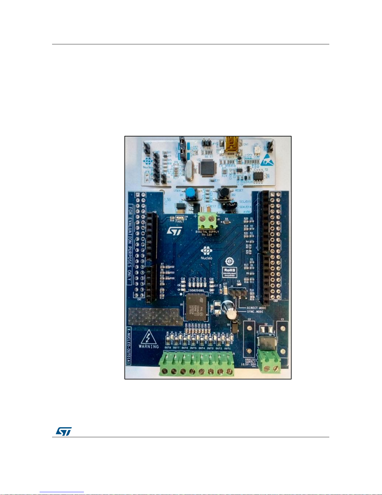
Figure 1: X-NUCLEO-OUT01A1 expansion board
Page 2

Contents
UM2209
2/17
DocID030568 Rev 1
Contents
1 Getting started ................................................................................. 5
1.1 Hardware requirements ..................................................................... 5
1.2 System requirements ........................................................................ 6
2 X-NUCLEO-OUT01A1 expansion board overview ......................... 7
2.1 Digital section .................................................................................... 7
2.2 Power section .................................................................................... 8
2.3 Direct access and synchronised access ........................................... 9
2.4 Powering and initializing the board .................................................. 10
3 Schematic diagrams ...................................................................... 11
4 Bill of materials .............................................................................. 13
5 References ..................................................................................... 15
6 Revision history ............................................................................ 16
Page 3

UM2209
List of tables
DocID030568 Rev 1
3/17
List of tables
Table 1: ISO8200BQ access modes .......................................................................................................... 9
Table 2: Bill of materials............................................................................................................................ 13
Table 3: Document revision history .......................................................................................................... 16
Page 4

List of figures
UM2209
4/17
DocID030568 Rev 1
List of figures
Figure 1: X-NUCLEO-OUT01A1 expansion board ..................................................................................... 1
Figure 2: X-NUCLEO-OUT01A1 plugged on an STM32 Nucleo board ...................................................... 5
Figure 3: STM32 Nucleo development board plus X-NUCLEO-OUT01A1 expansion board layout and
connection ................................................................................................................................................... 7
Figure 4: X-NUCLEO-OUT01A1 expansion board digital interface components ....................................... 8
Figure 5: X-NUCLEO-OUT01A1 expansion board power section components ......................................... 9
Figure 6: Schematic diagram (1 of 2) ....................................................................................................... 11
Figure 7: Schematic diagram (2 of 2) ....................................................................................................... 12
Page 5
UM2209
Getting started
DocID030568 Rev 1
5/17
1 Getting started
1.1 Hardware requirements
The X-NUCLEO-OUT01A1 is designed to be used with the following STM32 Nucleo boards
(visit www.st.com for further information):
NUCLEO-F103RB
NUCLEO-F302R8
NUCLEO-F401RE
Figure 2: X-NUCLEO-OUT01A1 plugged on an STM32 Nucleo board
The X-NUCLEO-OUT01A1 is plugged onto the matching Arduino® UNO R3 connector pins
on the STM32 Nucleo board.
Page 6

Getting started
UM2209
6/17
DocID030568 Rev 1
1.2 System requirements
To complete the system, you need:
a Windows® (version 7 or above) PC
a USB type A to mini-B USB cable to connect the STM32 Nucleo to the PC
the X-CUBE-OUT1 board firmware and software package installed on the user PC
Page 7

UM2209
X-NUCLEO-OUT01A1 expansion board overview
DocID030568 Rev 1
7/17
2 X-NUCLEO-OUT01A1 expansion board overview
The X-NUCLEO-OUT01A1 is equipped with the ISO8200BQ intelligent power switch (IPS),
featuring galvanic insulation for safe digital microcontroller interface and overcurrent and
over temperature protection for safe output load control.
Figure 3: STM32 Nucleo development board plus X-NUCLEO-OUT01A1 expansion board
layout and connection
The X-NUCLEO-OUT01A1 expansion board features:
Industrial programmable logic controller (PLC ) functionality for STM32 Nucleo
ISO8200BQ galvanic isolated octal high-side smart power solid state-relay:
voltage range: 10.5 V to 30 V
max. output current per channel I
OUT
= 0.7 A
status LEDs: Fault, thermal protection
Arduino® UNO R3 connector compatibility
compliance with EMC standards:
IEC61000-4-2: 8kV Contact Discharge and 15kV Air discharge
IEC61000-4-3: 4kV Discharge on output and supply line
IEC61000-4-5: 2kV Discharge on output and supply line
specifically designed for STM32 Nucleo development boards
RoHS compliance
As this is a digital output solution, each output state is managed at the
microcontroller level; indeed, the X-NUCLEO-OUT01A1 has no input stage and
no sensors can be connected to the expansion board.
2.1 Digital section
The digital section is associated with the STM32 interface and digital supply voltage to and
from the expansion board.
Page 8

X-NUCLEO-OUT01A1 expansion board overview
UM2209
8/17
DocID030568 Rev 1
Figure 4: X-NUCLEO-OUT01A1 expansion board digital interface components
The four Arduino® UNO R3 connectors:
allow expansion board ISO8200QB communication with the STM32 Nucleo board
microcontroller and access to STM32 peripheral and GPIO resources.
provide digital supply voltage between the STM32 Nucleo development board and the
X-NUCLEO-OUT01A1 expansion board, in either direction.
To provide an external digital supply:
close jumper JP5 between pins 2 and 3 on the STM32 Nucleo development board
connect a 7 V to 12 V supply at screw connector J2 on the X-NUCLEO-OUT01A1
expansion board
2.2 Power section
The power section involves the power supply voltage, load connection and Electromagnetic
compatibility (EMC) protections.
Page 9

UM2209
X-NUCLEO-OUT01A1 expansion board overview
DocID030568 Rev 1
9/17
Figure 5: X-NUCLEO-OUT01A1 expansion board power section components
For EMC:
a Transil™ diode SMC30J30CA is placed on VCC track to protect the ISO8200BQ
against surge discharge
for common mode surge testing, solder two single-layer capacitors C1 and C3 (not
included) at the predisposed locations
22 nF capacitors are included on the output lines for burst disturbance filtering
To supply the load, connect the supply voltage to the J1 2-way screw connector.
The load is connected to the 8-way output.
2.3 Direct access and synchronised access
Supplementary direct access and synchronized access routines are provided to allow
further evaluation of ISO8200BQ IC functionality.
Table 1: ISO8200BQ access modes
Access mode
Configuration
Direct access
connect the center pin of J4 to GND
Synchronous access
connect the center pin of jumper J4 to 3.3 V
Once the selection is configured, push the blue user button on the STM32 Nucleo
development board to begin evaluation.
Page 10

X-NUCLEO-OUT01A1 expansion board overview
UM2209
10/17
DocID030568 Rev 1
2.4 Powering and initializing the board
To start working with the X-NUCLEO-OUT01A1 board:
1. connect the micro-USB cable to your PC
2. download the firmware version onto the microcontroller
3. set the following jumper configurations on the STM32 Nucleo board:
Close jumpers SB62 and SB63
Open jumpers SB13 and SB14
4. connect the ISO8200BQ device supply voltage via J1 on the X-NUCLEO-OUT01A1
5. provide the digital supply voltage:
when connected to a PC: keep the micro-USB cable connected and close
jumper JP5 on the STM32 Nucleo board between pins 1 and 2.
in standalone mode: supply an external 7 V to 12 V via J2 on the X-NUCLEO-
OUT01A1 and close jumper JP5 on the STM32 Nucleo board between pins 2 and
3.
6. connect the load on the output connector
7. run the STM32 and push the blue button on STM32 Nucleo board to select the
example provided in the firmware package
Page 11

UM2209
Schematic diagrams
DocID030568 Rev 1
11/17
3 Schematic diagrams
Figure 6: Schematic diagram (1 of 2)
Vcc supply
GND_DEC
ISO_IN8
ISO_IN7
ISO_IN6
ISO_IN5
ISO_IN4
ISO_IN3
ISO_IN2
ISO_IN1
ISO_LOAD
ISO_SYNC
ISO_OUT EN
GND_DEC
Vcc supply
ISO_IN8
ISO_IN7
ISO_IN6
ISO_IN5
ISO_IN4
ISO_IN3
ISO_IN2
ISO_IN1
ISO_LOAD
ISO_SYNC
ISO_OUT EN
GND_DEC
Vcc supply
ISO_IN8
ISO_IN7
ISO_IN6
ISO_IN5
ISO_IN4
ISO_IN3
ISO_IN
ISO_IN1
ISO_LOAD
ISO_SYNC
ISO_OUT EN
3v3
3v3
R294k7
R24
8k2
C1610pF/6.3V
22nF/50V
C22
R18
47k
C1010pF/6.3V
D11
R35
47k
R25
8k2
22nF/50V
C21
U1
ISO8200BQ
GNDdd
1
NC
2
3
GND1
OUT8a4OUT8b5OUT7a6OUT7b7OUT6a8OUT6b9OUT5a10OUT5b11OUT4a12OUT4b13OUT3a14OUT3b15OUT2a16OUT2b17OUT1a18OUT1b
19
Vdd
20
OUT EN
21
SYNC
22
LOAD
23
IN124IN225IN326IN427IN528IN629IN730IN8
31
FAULT
32
36
TAB Vcc
GND2
33
34
GND3
GND4
35
R19
47k
C1110pF/6.3V
C1710pF/6.3V
R16
470R
D9
C5
100nF/50V
D8
R26
8k2
C20
22nF/50V
R304k7
47uF/10V
C27
R32
47k
D10
C1210pF/6.3V
C26
22nF/50V
C1810pF/6.3V
2.2uF/50V MLCC
C7
D7
R27
8k2
22nF/50V
C19
R21
8k2
22nF/50V
C25
C1310pF/6.3V
D4
RED LED
R33
47k
D6
R28
8k2
R22
8k2
C1410pF/6.3V
22nF/50V
C24
R31
47k
C810pF/6.3V
J5
CON8
1234567
8
D5
D12
R23
8k2
C23
22nF/50V
C1510pF/6.3V
R20
47k
R17
47k
R34
47k
C9
10pF/6.3V
220nF/10V
C28
10uF/63V
C6
+
Page 12

Schematic diagrams
UM2209
12/17
DocID030568 Rev 1
Figure 7: Schematic diagram (2 of 2)
Analog supply
10.5 V - 30 V
Arduino Connectors
Digital supply
7V - 12V
Morpho Connectors
PB10
PB4
PB5
PB3
PA2
PA3
PA0
PA1
PA4
PB0
PC1
PC0
PB8
PB9
PB6
PC7
ALTERNATE USE
ALTERNATE USE
ALTERNATE USE
ALTERNATE USE
DEFAULT
DEFAULTDEFAULT
DEFAULT
DEFAULT
DEFAULT
DEFAULT
DEFAULT
DEFAULT
DEFAULT
DEFAULT
DEFAULT
GND
3V3
Vcc supply
GND_DEC
AVDD
D4
GND
EARTH
VIN
VIN
A0
ISO_IN3
D0
A1
A2
A3
A4
ISO_SYNC
A5
ISO_IN2
ISO_OUT EN
ISO_IN6
ISO_IN4
D15
D14
D10
NRST
IOREF
5V
D8
ISO_IN1
D5
ISO_IN5
ISO_IN8
ISO_IN7
D9
D1
ISO_SYNC
ISO_OUT EN
D3
D6
ISO_IN5
ISO_IN6
D7
D2
D13
D12
D11
ISO_LOAD
NC1
D15
D14
D13
D12
D11
D10
AVDD
D9
D8
D0
D1
D2
D3
D4
D5
D6
D7
5V
NRST
NC1
IOREF
3V3
A2
A3
A4
A5
VIN
GND
A1
A0
GND_DEC
Vcc supply
ISO_IN8
ISO_IN7
ISO_IN6
ISO_IN5
ISO_IN4
ISO_IN3
ISO_IN2
ISO_IN1
ISO_LOAD
ISO_SYNC
ISO_OUT EN
EARTH
GND_DEC
Vcc supply
ISO_IN8
ISO_IN7
ISO_IN6
ISO_IN5
ISO_IN4
ISO_IN3
ISO_IN
ISO_IN1
ISO_LOAD
ISO_SYNC
ISO_OUT EN
3v3
3v3
C3
4.7nF/3kV N.M
D1
SMC30J30CA
R6100R
CN9
CON8
1
2
3
4
5
6
7
8
D2
STPS1H100A
J2
M2VITE
1
2
J4
ISO_DRIVING
1
3
2
R8100R
CN5
CON10
1
2
3
4
5
6
7
8
9
10
C2
2.2uF/50V
R13100R
R10100R
D3
BAT48JFILM
R9100R
CN8
CON6
1
2
3
4
5
6
CN10
CON38
1 2
3 4
5 6
7 8
9 10
11 12
13 14
15 16
17 18
19 20
21 22
23 24
25 26
27 28
29 30
31 32
33 34
35 36
37 38
R3100R N.M.
R5100R N.M.
R1100R
R4100R N.M.
J1
Main voltage
1
2
R15100R
C4
10pF/10V
R2100R
CN6
CON8
1
2
3
4
5
6
7
8
C1
4.7nF/3kV N.M.
R11100R N.M.
R14100R
CN7
CON38
1 2
3 4
5 6
7 8
9 10
11 12
13 14
15 16
17 18
19 20
21 22
23 24
25 26
27 28
29 30
31 32
33 34
35 36
37 38
R12100R
R7100R
Page 13

UM2209
Bill of materials
DocID030568 Rev 1
13/17
4 Bill of materials
Table 2: Bill of materials
Item
Quantity
Reference
Part/Value
Description
Manufacturer
Order code
1
8
C19,C20,C21,C22,C23,
C24,C25,C26
22nF, 50V,
+/- 10%
Ceramic
MLCC
Kemet
C0603C223
K1RACTU
2
12
C4,C8,C9,C10,C11,C1
2,C13,C14,C15,C16,C1
7,C18
10pF, 50V,
+/-5%
Ceramic
capacitor
MULTICOMP
MCMT15N1
00F100CT
3
1
C6
10uF, 63V
, +/- 10%
Low ESR
Rubycon
63YXF10M5
X11
4 1 C27
47uF, 10V,
+/- 10%
MLCC Low
ESR
Murata
GRM31CR6
1A476KE15
L
5 1 C28
220nF,
10V, +/-
10%
Kemet
C0603C224
K8RACTU
6
1
C5
100nF,
50V, +/-
10%
Murata
GCM188R71
H104KA43D
7 2 C1,C3
4.7nF, 3kV
,
Vishay / BC
Components
VY1472M63
Y5UQ63V0
8 2 C2,C7
2.2uF,
100V, +/-
10%
MLCC Low
ESR
TDK
C3225X7R2
A225K230A
B
9
1
D1
Transil
series diode
ST
SMC30J30C
A
10 1 D2
High
Voltage
Power
Schottky
Rectifier
ST
STPS1H100
A
11 1 D4
CHIPLED
OSRAM Opto
Semiconducto
rs
LR Q396
12
8
D5,D6,D7,D8,D9,D10,
D11,D12
CHIPLED
OSRAM Opto
Semiconducto
rs
LT Q39G-
Q1S2-25-1
13 1 D3
Small signal
Schottky
diodes
ST
BAT48JFILM
14 1 CN5
Samtec
SSQ-110-
03-L-S
15 2 CN6,CN9
Samtec
SSQ-108-
03-L-S
16 1 CN8
Samtec
SSQ-106-
03-L-S
17 1 J5
RS
Page 14

Bill of materials
UM2209
14/17
DocID030568 Rev 1
Item
Quantity
Reference
Part/Value
Description
Manufacturer
Order code
18 2 J1,J2
RS
19 1 J4
TE
Connectivity
87224-3
20 2 CN7,CN10
Samtec
SSQ-119-
04-L-D
21 1 R16
470R, +/-
5%
Bourns
CR0603-JW-
471GLF
22 2 R29,R30
4k7, +/-5%
Bourns
CR0603-JW-
472GLF
23
8
R21,R22,R23,R24,R25,
R26,R27,R28
8.2K, +/1%
TE
Connectivity
CRG0805F8
K2
24
11
R1,R2,R6,R7,R8,R9,R
10,R12,R13,R14,R15
100R, +/-
5%
Bornus
CR0603-JW-
101GLF
25 4 R3,R4,R5,R11
100R, +/-
5%
Bornus
CR0603-JW-
101GLF
26
9
R17,R18,R19,R20,R31,
R32,R33,R34,R35
47k, +/-5%
Bourns
CR0603-JW-
473GLF
27 1 U1
Galvanic
isolated
octal highside smart
power solid
state-relay
ST
ISO8200BQ
Page 15

UM2209
References
DocID030568 Rev 1
15/17
5 References
The following resources are all readily available on www.st.com
1. ISO8200BQ datasheet
2. X-CUBE-OUT1 user manual
3. X-NUCLEO-PLC01A1 user manual
4. X-NUCLEO-IDW01M1 user manual
5. ST-PLC databrief
6. STM32 Nucleo-64 board user manual
Page 16

Revision history
UM2209
16/17
DocID030568 Rev 1
6 Revision history
Table 3: Document revision history
Date
Version
Changes
09-Jun-2017
1
Initial release.
Page 17

UM2209
DocID030568 Rev 1
17/17
IMPORTANT NOTICE – PLEASE READ CAREFULLY
STMicroelectronics NV and its subsidiaries (“ST”) reserve the right to make changes, corrections, enhancements, modifications , and
improvements to ST products and/or to this document at any time without notice. Purchasers should obtain the latest relevant information on ST
products before placing orders. ST products are sold pursuant to ST’s terms and conditions of sale in place at the time of order
acknowledgement.
Purchasers are solely responsible for the choice, selection, and use of ST products and ST assumes no liability for application assistance or the
design of Purchasers’ products.
No license, express or implied, to any intellectual property right is granted by ST herein.
Resale of ST products with provisions different from the information set forth herein shall void any warranty granted by ST for such product.
ST and the ST logo are trademarks of ST. All other product or service names are the property of their respective owners.
Information in this document supersedes and replaces information previously supplied in any prior versions of this document.
© 2017 STMicroelectronics – All rights reserved
 Loading...