

Page 1
September 2015
DocID028304 Rev 1
1/28
www.st.com
UM1943
User manual
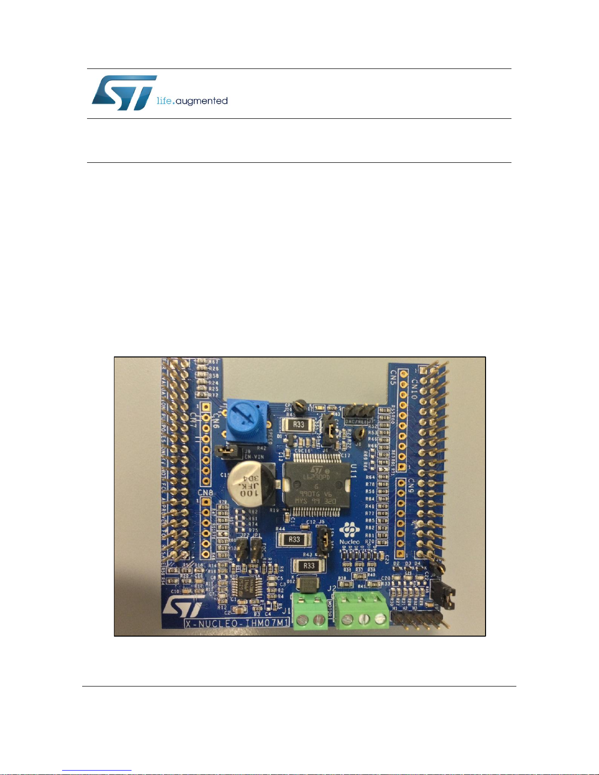
Getting started with the X-NUCLEO-IHM07M1 motor driver
expansion board based on the L6230 for STM32 Nucleo
Introduction
The X-NUCLEO-IHM07M1 is a three-phase brushless DC motor driver expansion board based on the
L6230 for STM32 Nucleo. It provides an affordable and easy-to-use solution for driving three-phase
brushless DC motors in your STM32 Nucleo project. The X-NUCLEO-IHM07M1 is compatible with the
ST morpho connector and supports the addition of other boards which can be stacked onto a single
STM32 Nucleo board. The user can also mount the Arduino UNO R3 connector. The X-NUCLEOIHM07M1 is fully configurable and ready to support different closed loop control based on sensor or
sensorless mode control, and it is compatible with three shunt or single shunt current sense measuring.
The driver used on this STM32 Nucleo expansion board is the L6230, a DMOS fully-integrated driver for
three-phase brushless PMSM motors, assembled in a PowerSO36 package, with overcurrent and
thermal protection. This user manual describes the procedure to configure the X-NUCLEO-IHM07M1
expansion board to operate with an STM32 Nucleo board.
Figure 1: X-NUCLEO-IHM07M1 three-phase brushless DC motor driver expansion board based on L6230 for
STM32 Nucleo
Page 2

Contents
UM1943
2/28
DocID028304 Rev 1
Contents
1 System introduction ......................................................................... 3
1.1 Main characteristics .......................................................................... 3
1.2 Target applications ............................................................................ 3
2 Getting started .................................................................................. 4
2.1 System architecture .......................................................................... 4
2.2 Building the system ........................................................................... 4
2.2.1 Hardware settings ............................................................................... 5
3 Board schematic ............................................................................. 10
4 Circuit description .......................................................................... 18
4.1 Power section – L6230 driver with integrated three-phase bridge ... 18
4.2 Power section – Overcurrent detection (OCP) and current sensing
measurement ............................................................................................... 19
4.3 Analog section – Hall/Encoder motor speed sensor ........................ 21
4.4 Analog section – BEMF detection circuit ......................................... 21
4.5 Analog section – Bus voltage and temperature sensing circuit ....... 21
5 BOM (bill of material) ..................................................................... 23
6 Revision history .............................................................................. 27
Page 3

UM1943
System introduction
DocID028304 Rev 1
3/28
1 System introduction
1.1 Main characteristics
The list below provides the board specification data and the main parameters for the XNUCLEO-IHM07M1 expansion board:
Three-phase driver board for BLDC/PMSM motors
Nominal operating voltage range from 8 V to 48 V DC
2.8 A output peak current (1.4 A
RMS
)
Operating frequency up to 100 kHz
Non dissipative overcurrent detection and protection
Cross-conduction protection
Thermal measuring and overheating protection
Full compatibility with ST Six Step or ST FOC control algorithms
Full support for sensor and sensorless mode
3-shunt and 1-shunt configurable jumpers for motor current sensing
Hall/Encoder motor sensor connector and circuit
Debug connector for DAC, GPIOs, etc.
Potentiometer available for speed regulation
Fully populated board conception with test points
User LED
Compatible with STM32 Nucleo boards
Equipped with ST morpho connectors
RoHS compliant
PCB type and size:
PCB material: FR-4
4-layer layout
Copper thickness: 70 μm (external layer), 35 μm (internal layer)
Total dimensions of the board: 70 mm x 66 mm
1.2 Target applications
Low voltage PMSM motor driver
Low power fans
Power tools
Industrial drives
Page 4
Getting started
UM1943
4/28
DocID028304 Rev 1
2 Getting started
2.1 System architecture
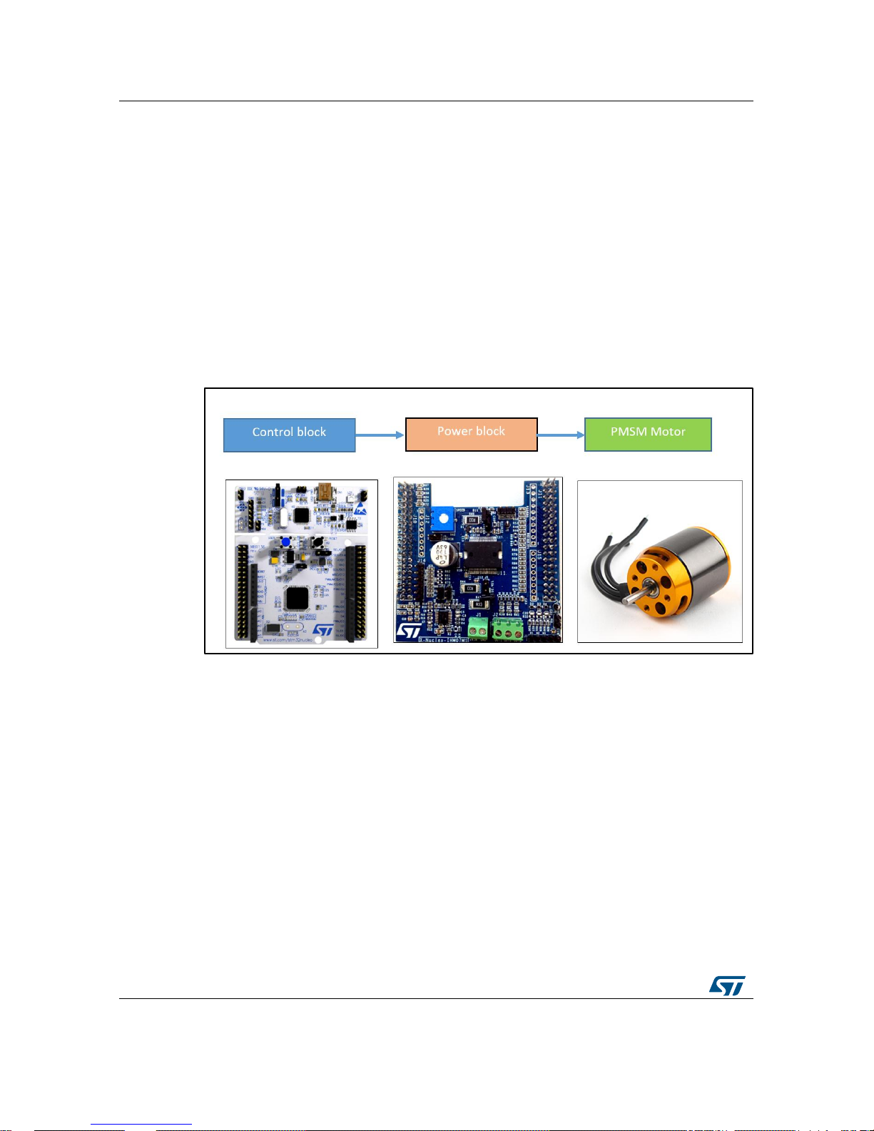
A generic motor control system can be schematized in three main blocks (see Figure 2:
"Overall system architecture"):
Control block - its main task is to accept user commands and drive a motor. The X-
NUCLEO-IHM07M1 is based on the STM32 Nucleo board, which provides all digital
signals to properly implement motor driver control.
Power block - it is based on three-phase inverter topology. The core of the power
block is the L6230 driver, which contains all the necessary active power and analog
components to perform low voltage PMSM motor control.
Motor - the X-NUCLEO-IHM07M1 is able to properly drive a low voltage BLDC/PMSM
motor.
Figure 2: Overall system architecture
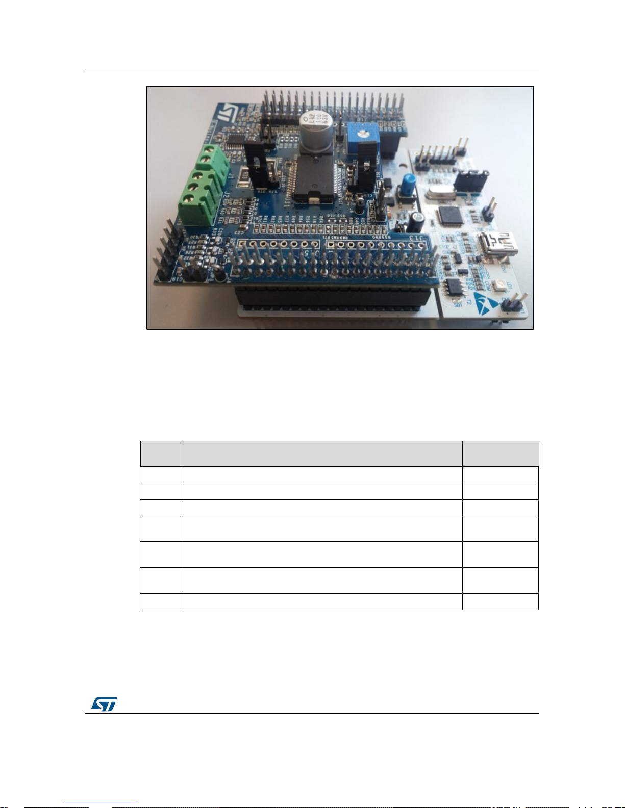
2.2 Building the system
The X-NUCLEO-IHM07M1 expansion board is a complete hardware development platform
(Power block) for the STM32 Nucleo board, for evaluating a motor control solution for a
single BLDC/PMSM motor. For normal board operation, it must be connected to an STM32
Nucleo board (Control block) through the ST morpho connector, as shown in the image
below.
Page 5
UM1943
Getting started
DocID028304 Rev 1
5/28
Figure 3: X-NUCLEO-IHM07M1 plugged on STM32 Nucleo
The interconnection between the STM32 Nucleo and the X-NUCLEO-IHM07M1 has been
designed for full-compatibility with many STM32 Nucleo boards and no solder bridge
modification is required. When stacked, the system is ready to operate with the connection
of a BLDC/PMSM motor. For proper use, please respect the hardware and software
settings. For the software details, refer to the X-CUBE-SPN7 software expansion
documents available on www.st.com.
2.2.1 Hardware settings
Table 1: Jumper settings
Jumper
Permitted configurations
Default
condition
JP1
Selection for pull-up insertion (BIAS) in current sensing circuit
OPEN
JP2
Selection for op amp gain modification in current sensing circuit
OPEN
JP3
Selection for pull-up enabling in Hall/Encoder detection circuit
CLOSED
J9
Selection to supply the STM32 Nucleo board through the X-NUCLEOIHM07M
(1)
OPEN
J5
Selection for single/three shunt configuration. Set to single shunt by
default
2-3 CLOSED
J6
Selection for single/three shunt configuration. Set to single shunt by
default
2-3 CLOSED
J7
Debug connector for DAC. Available for probe connection
OPEN
Notes:
(1)
It is recommended to REMOVE jumper J9 before power-on on J1
Page 6
Getting started
UM1943
6/28
DocID028304 Rev 1
With J9 closed, it is mandatory not to exceed 12 V DC on the J1 connector to avoid
damage to the STM32 Nucleo board.
Jumper JP5 (STM32 Nucleo board) MUST be connected between pin 2 and 3 to enable
the STM32 Nucleo external power supply.
Table 2: Screw terminal table
Screw terminal
Function
J1
Motor power supply input (8 V- 48 V DC)
J2
3-phase motor connector
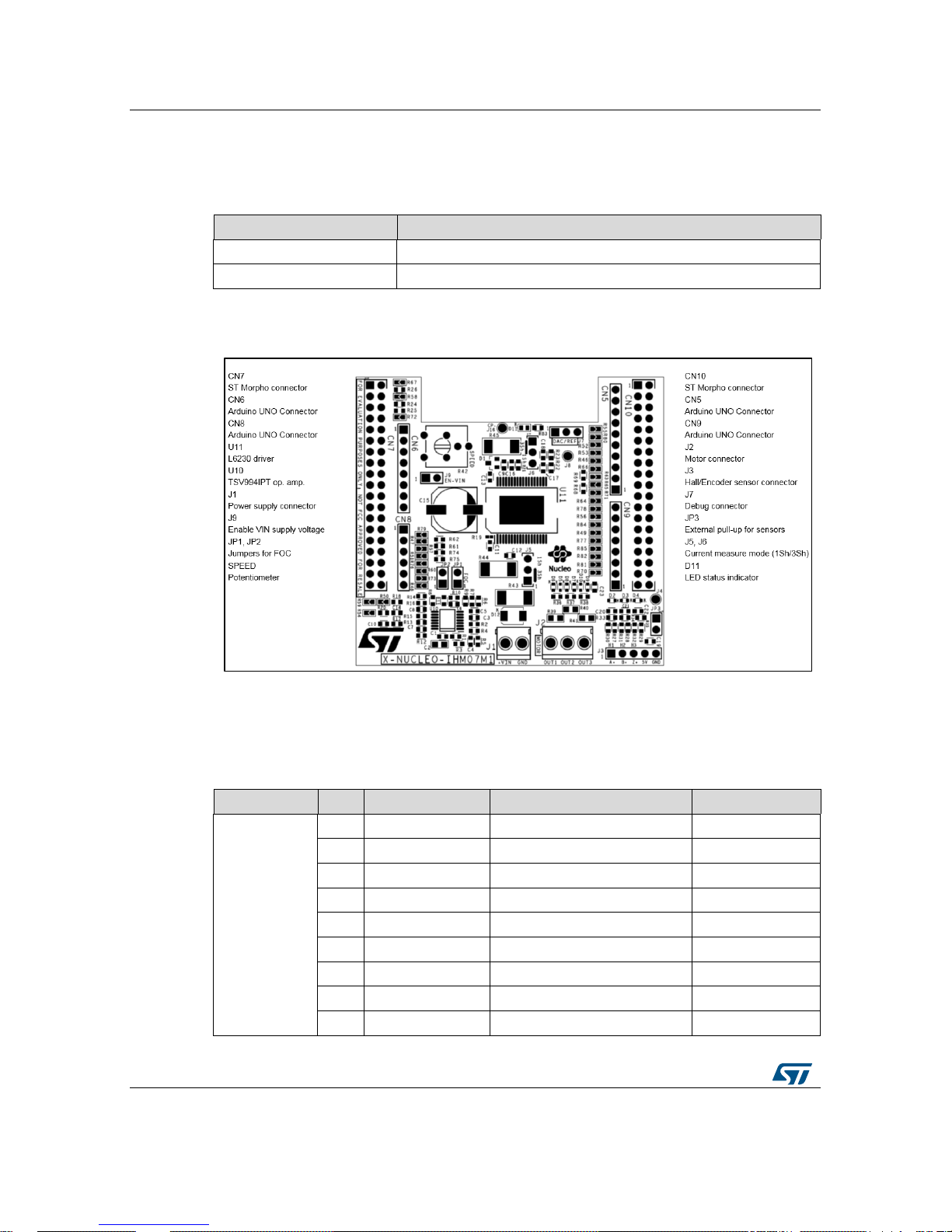
Figure 4: X-NUCLEO-IHM07M1 – top layer with silk-screen
The X-NUCLEO-IHM07M1 expansion board is equipped with the ST morpho connector,
male pin headers (CN7 and CN10) accessible on both sides of the board. They can be
used to connect the power board to the STM32 Nucleo board. All signals and power pins of
the MCU are available on the ST morpho connector. For further details, please refer to user
manual UM1724 (5.12 STMicroelectronics morpho connector) available on www.st.com.
Table 3: ST morpho connector table
Connector
Pin
Default
Signal
Solder bridge
CN7
1
PC10
Enable_CH1-L6230
R58
2
PC11
Enable_CH2-L6230
R67
3
PC12
Enable_CH3-L6230
R72
4
PD2 5 VDD 6 E5V
7
BOOT0
8
GND
9
NC/PF6
Page 7
UM1943
Getting started
DocID028304 Rev 1
7/28
Connector
Pin
Default
Signal
Solder bridge
10
NC
11
NC/PF7
12
IOREF
13
PA13
14
RESET
15
PA14
16
+3V3
17
PA15
Encoder A/Hall H1
R79
18
+5V
Encoder/Hall PS voltage
19
GND
20
GND
21
PB7
22
GND
23
PC13
Blue button
24
VIN
J9
25
PC14
26
NC
27
PC15
28
PA0
Curr_fdbk_PhA
R47
29
PH0/PF0/PD0
30
PA1
VBUS_sensing
R51
31
PH1/PF1/PD1
32
PA4
DAC_Ch
R76 N.M.
33
VLCD/VBAT
34
PB0
BEMF2_sensing
R60
35
PC2
Temperature feedback
R54
36
PC1 or PB9
(1)
Curr_fdbk_PhB
R48
37
PC3
BEMF1_sensing
R59
38
PC0 or PB8
(2)
Curr_fdbk_PhC
R50
CN10
1
PC9 2 PC8
3
PB8 4 PC6 5 PB9
6
PC5
7
AVDD
8
U5V
(3)
Page 8
Getting started
UM1943
8/28
DocID028304 Rev 1
Connector
Pin
Default
Signal
Solder bridge
9
GND
10
NC
11
PA5
(4)
GPIO/DAC/PWM
R80
12
PA12
CPOUT
R52
13
PA6
(5)
DIAG/ENABLE/BKIN1
R53
14
PA11
DIAG/ENABLE/BKIN2
R46
15
PA7
(6)
BEMF3_sensing
R63
16
PB12
17
PB6
18
PB11/NC
19
PC7
20
GND
21
PA9
VH_PWM
R64
22
PB2
LED RED
R83
23
PA8
UH_PWM
R56
24
PB1
POTENTIOMETER
R78
25
PB10
Encoder Z/Hall H3
R84
26
PB15
(7)
BEMF3_sensing
R66
27
PB4
CURRENT REF
R77
28
PB14
(8)
DIAG/ENABLE/BKIN1
R49
29
PB5
GPIO/DAC/PWM
R85
30
PB13
(9)
GPIO/DAC/PWM
R82
31
PB3
Encoder B/Hall H2
R81
32
AGND
33
PA10
WH_PWM
R70
34
PC4
35
PA2
36
NC/PF5
37
PA3
38
NC/PF4
Notes:
(1)
Please refer to Table 9: Solder bridges in user manual UM1724 for further details
(2)
Please refer to Table 9: Solder bridges in user manual UM1724 for further details
(3)
U5V is 5 V power from ST-LINK/V2-1 USB connector and it rises before +5 V
(4)
For STM32F302-Nucleo only:
- pin PA5 is on CN10/pin 30 and PB13 is on CN10/pin 11
- pin PA6 is on CN10/pin 28 and PB14 is on CN10/pin 13
- pin PA7 is on CN10/pin 26 and PB15 is on CN10/pin 13
Page 9

UM1943
Getting started
DocID028304 Rev 1
9/28
(5)
For STM32F302-Nucleo only:
- pin PA5 is on CN10/pin 30 and PB13 is on CN10/pin 11
- pin PA6 is on CN10/pin 28 and PB14 is on CN10/pin 13
- pin PA7 is on CN10/pin 26 and PB15 is on CN10/pin 13
(6)
For STM32F302-Nucleo only:
- pin PA5 is on CN10/pin 30 and PB13 is on CN10/pin 11
- pin PA6 is on CN10/pin 28 and PB14 is on CN10/pin 13
- pin PA7 is on CN10/pin 26 and PB15 is on CN10/pin 13
(7)
For STM32F302-Nucleo only:
- pin PA5 is on CN10/pin 30 and PB13 is on CN10/pin 11
- pin PA6 is on CN10/pin 28 and PB14 is on CN10/pin 13
- pin PA7 is on CN10/pin 26 and PB15 is on CN10/pin 13
(8)
For STM32F302-Nucleo only:
- pin PA5 is on CN10/pin 30 and PB13 is on CN10/pin 11
- pin PA6 is on CN10/pin 28 and PB14 is on CN10/pin 13
- pin PA7 is on CN10/pin 26 and PB15 is on CN10/pin 13
(9)
For STM32F302-Nucleo only:
- pin PA5 is on CN10/pin 30 and PB13 is on CN10/pin 11
- pin PA6 is on CN10/pin 28 and PB14 is on CN10/pin 13
- pin PA7 is on CN10/pin 26 and PB15 is on CN10/pin 13
Page 10

Board schematic
UM1943
10/28
DocID028304 Rev 1
3 Board schematic
Figure 5: X-NUCLEO-IHM07M1 schematic (1 of 8)
Vshunt_3_GND
Vshunt_2_GND
Vshunt_1_GND
Externaloperational-amplifier
Overall AV=1.53
3V3
3V3
3V3
3V3
3V3
3V3
3V3
Vshunt_1
Curr_fdbk1
Curr_fdbk2
CP+
Vshunt_2
Curr_fdbk3
Vshunt_3
C8
N.M. 100pF/6.3V
JP1
FOC
R11
2.2k
C4
N.M. 100p F/6.3V
R13
680
C1
100nF10V
R9
2.2k
-
+
U10C
TSV994IPT
10
9
8
4
11
-
+
U10D
TSV994IPT
12
13
14
4
11
R10 2.2k
C3
680pF 10V
0 3R
R15
2.2k
R1
2.2k
C7
680pF 10V
R5 2.2k
R4
2.2k
R14
0
R8
0
R2
680
R12
2.2k
C5
680pF 10V
-
+
U10B
TSV994IPT
5
6
7
4
11
-
+
U10A
TSV994IPT
3
2
1
4
11
R7
680
R16
2.2k
R6
2.2k
C6
N.M. 100pF/6.3V
JP2 FOC
C2
4.7uF 10V
GSPG03092015DI0955
Page 11

UM1943
Board schematic
DocID028304 Rev 1
11/28
Figure 6: X-NUCLEO-IHM07M1 schematic (2 of 8)
HALL/ENCODER SENSOR
5V
GND
A+/H1
B+/H2
Z+/H3
3V3 3V3
5V
A+/H1
B+/H2
Z+/H3
R30
1k8
JP3
JUMPER
C20
10pF10V
R32
1k8 R34
4K7N.M.
R31
1k8
R33
4K7N.M.
R29
10k
J3
Striplinem.1x5
1
2
3
4
5
C22
10pF10V
R28
10k
R27
10k
D4
BAT30KFILM
D3
BAT30KFILM
D2
BAT30KFILM
C19
100n
R35
4K7N.M.
J4
RING
1
C21
10pF10V
SPEED REGULATION
SPEE D
3V3
SPEE D
R42
100K
SHUNT RESISTOR
Vshunt_1_GND
Vshunt_2_GND Vshunt_3_GND
Vshunt_1 Vshunt_2 Vshunt_3
R45
0.331W
R44
0.331W
R43
0.331W
RS model 742-8420
Placed near the L6230 driver
3V3
Temperature feedba ck
R19
NTC 10K
2
1
R20
4K7
C10
10nF 10V
VBUS SENSOR
VB US_SENS
VIN+
VBUS
C14
4.7n F/10V
R18
9.31K1%
R17
169K1%
GSPG03092015DI1000
Page 12

Board schematic
UM1943
12/28
DocID028304 Rev 1
Figure 7: X-NUCLEO-IHM07M1 schematic (3 of 8)
L6230 DMOS d
river for three-phase b
rushless DC motor
POWER CONNEC
TOR
OUT1
OUT2
OUT3
SENS1
SENS2
SENS3
CPOUT
IN1
EN1
EN3
IN3
EN2
IN2
CP+
CP-
VIN+
3V3
3V3
Vshunt_2
EN3
IN3
EN2
IN2
DIAG/EN
CURRENTREF
CPOUT
CP+
IN1
EN1
R21
33K
J16
RING
1
R25
39k
R23
10K
roto
M
2
J
1
2
3
C13
100nF/100V
C17
1nF/6.3V
D1
SMBD7000
1
2
3
C18
10n-N.M.
C15
100uF, 63V
C12
10n100V
U11
L6230P D
IN19CPOUT
24
VSA
4
N.C.
3
N.C.
2
GND
1
OUT3
32
N.C.
31
VBOOT
30
EN3
29
CP-
28
VCP
7
CP+
13
N.C.
14
OUT1
15
N.C.
16
N.C.
17
GND18GND
19
N.C.
20
N.C.
21
EN1
10
SENS1
12
N.C.
23
N.C.
6
IN2
26
SENS2
8
SENS3
25
EN2
27
IN3
11
OUT2
5
DIAG/EN
22
VSB
33
N.C.
34
N.C.
35
GND
36
EP
37
C16
100n,6.3V
R22
10K
C9
220nF, 16V
C11
100nF/100V
R26
39k
D12
SMBJ48A-TR
R24
39k
J1
CON2
1
2
GSPG03092015DI1005
Page 13

UM1943
Board schematic
DocID028304 Rev 1
13/28
Figure 8: X-NUCLEO-IHM07M1 schematic (4 of 8)
3Sh
1Sh
3Sh
1Sh
BEMF
DETECTION
- SIXSTEP
SINGLE/THREE SHUNT CONFIGURATION
OUT1
OUT2
OUT3
GPIO_BEMF
GPIO_BEMF
GPIO_BEMF
BEMF1
BEMF3
3V3
3V3
3V3
3V3
GPIO_BEMF
BEMF1
BEMF2
GPIO_BEMF
GPIO_BEMF
BEMF3
Vshunt_3
SENS3
Vshunt_2
Vshunt_1
SENS1
Vshunt_2
R39
10k
J6
CON3
123
R36
2.2k
D10
BAT30KFILM
D6
BAT30KFILM
R41
10k
J5
CON3
123
D9
BAT30KFILM
D5
BAT30KFILM
D8
BAT30KFILM
R38
2.2k
C23
0.1uF/6.3V
R40
10k
D7
BAT30KFILM
R37
2.2k
GSPG03092015DI1010
Page 14

Board schematic
UM1943
14/28
DocID028304 Rev 1
Figure 9: X-NUCLEO-IHM07M1 schematic (5 of 8)
F302
PWM
PA8-UH
PA6-BKIN
PA9-VH
PA10-WH
PC12
PC11
PC10
PA11
DIAG/EN
IN1
EN1
IN2
EN2
IN3
EN3
C10_14
C10_28
C10_13
C10_23
C7_1
C10_21
C7_2
C10_33
C7_3
R58
0
R46
0
R640R70
0
R67
0
R53
0
R72
0
R56
0
R49
0
HALL/E
NCODE
R SENSOR
PA15 - Enc. A/H1
PB3 - Enc. B/H2
PB10 - Enc. Z/H3
C7_17
C10_31
C10_25
Z+/H3
A+/H1
B+/H2
R81
0
R790R84
0
DAC/REF
F302
PA5/PB13
PA4- DAC
PB4-PWM
PA5 - DAC
PB5-DAC PWM
CURR
ENT REF
C7_32
C10_27
C10_11
C10_30
C10_29
0 28R
J8
RING
1
0 08R
J7
Stripline m. 1
x3
123
0 77R
R76
0-N.M.
0 58R
Currents
F302
EmbPGA
PA0 - PhA
PC1 - PhB
PC0 - PhC
PA1 - BUSV
PC2 - Temp. Sen s.
PA1 - EmbPGA
PA7 - EmbPGA
PB0 - EmbPGA
3V3
C7_28
C7_38
C7_35
Curr_fdbk1
Curr_fdbk2
Curr_fdbk3
VBUS
Temperature feedba
ck
C7_30
C10_15
C7_34
Vshunt_1
Vshunt_2
C10_26
Vshunt_3
C7_36
C7_30
0 74R
R73 0
0 45R
R69
N.M.13K 1%
R65
0
R74
N.N. 4.99K
R68
N.N. 4.99K
R61
N.N. 4.99K
R71 0-N.M.
0 15R
0 84R
0 05R
0 75R
R62
N.M.13K 1%
R75
N.M.13K 1%
GSPG03092015DI1015
Page 15

UM1943
Board schematic
DocID028304 Rev 1
15/28
Figure 10: X-NUCLEO-IHM07M1 schematic (6 of 8)
STM32 NUCLEO PART USED
PC13 - START/STOP (B1 BUTTON)
RESET - MCU RST (B2 BUTTON)
VIN
VIN+
C7_24
J9
JUMPER VIN 3A
12
Open by default J27 on:
1) 12 VMAX on J26
2) JP5 (Nucleo pin 2, 3)
2) JP1 (Nucleo) removed
USER
PB1
PB2
C10_24
C10_22
SPEED
D11
RED
0 87R
R83
510
BEMF six STEP
F302
PC9 - GPIO
PC3 - ADC
PB0 - ADC
PA7 - ADC
PA12- TIM1 ETR
C10_12
C10_1
C7_37
C7_34
C10_15
C10_26
CPOUT
GPIO_BEMF
BEMF1
BEMF2
BEMF3
0 25R
0 66R
0 95R
0 36R
0 06R
0 55R
GSPG03092015DI1020
Page 16

Board schematic
UM1943
16/28
DocID028304 Rev 1
Figure 11: X-NUCLEO-IHM07M1 schematic (7 of 8)
ARDUINO/
ST
MORPHO
CONNECTOR
C7_1
C7_3
C7_5
C7_7
C7_13
C7_15
C7_17
C7_19
C7_21
C7_23
C7_25
C7_27
C7_29
C7_31
C7_33
C7_35
C7_37
C7_14
C6_3
C7_16
C7_18
C6_5
C7_20
C7_22
C7_24
C6_8
C7_28
C8_1
C7_38
C8_6
C7_36
C8_5
C7_34
C8_4
C7_30
C8_2
C7_32
C8_3
C7_2
C7_4
E5V C7_6
C7_8
C10_3
C5_10
C10_7
C5_8
C10_9
C5_7
C10_11
C5_6
C10_13
C5_5
C10_15
C5_4
C10_17
C5_3
C10_19
C5_2
C10_21
C5_1
C10_5
C5_9
C10_35
C9_2
C10_29
C9_5
C10_31
C9_4
C10_25
C9_7
C10_33
C9_3
C10_27
C9_6
C10_23
C9_8
C10_37
C9_1
C10_1
C10_2
C10_4
C10_6
C10_8
C10_10
C10_12
C10_14
C10_16
C10_18
C10_20
C10_22
C10_24
C10_26
C10_28
C10_30
C10_32
C10_34
C10_36
C10_38
C7_9
C7_11
C7_12
C6_1 N.C.
C6_2 +3V3
C6_6
N.C. C7_10
C6_7
C7_26
C6_4
C7_18
3V3
5V
CN6
1
234
5
678
CN5
123456789
10
CN10
123
4
5
6
789
10
11
12
131415
16
17
18
192021
22
23
24
25262728293031323334353637
38
CN7
12345
678
91011
12
13
14
151617
18
19
20
212223
24
25
26
2728293031323334353637
38
CN8
1
2
345
6
CN9
12345
6
7
8
GSPG03092015DI1410
Page 17

UM1943
Board schematic
DocID028304 Rev 1
17/28
Figure 12: X-NUCLEO-IHM07M1 schematic (8 of 8)
L6230 DMOS d
river for three-phase b
rushless DC motor
POWER CONNEC
TOR
OUT1
OUT2
OUT3
SENS1
SENS2
SENS3
CPOUT
IN1
EN1
EN3
IN3
EN2
IN2
CP+
CP-
VIN+
3V3
3V3
Vshun t_2
EN3
IN3
EN2
IN2
DIAG/EN
CURRENT REF
CPOUT
CP+
IN1
EN1
R21
33K
J16
RING
1
R25
39k
R23
10K
rotoM 2J
1
2
3
C13
100nF/100V
C17
1nF/6.3V
D1
SMBD7000
1
2
3
C18
10n-N.M.
C15
100uF,63V
C12
10n100V
U11
L6230PD
IN19CPOUT
24
VSA
4
N.C.
3
N.C.
2
GND
1
OUT3
32
N.C.
31
VBOOT
30
EN3
29
CP-
28
VCP
7
CP+
13
N.C.
14
OUT1
15
N.C.
16
N.C.
17
GND
18
GND
19
N.C.
20
N.C.
21
EN1
10
SENS1
12
N.C.
23
N.C.
6
IN2
26
SENS2
8
SENS3
25
EN2
27
IN3
11
OUT2
5
DIAG/EN
22
VSB
33
N.C.
34
N.C.
35
GND
36
EP
37
C16
100n,6.3V
R22
10K
C9
220nF,16V
C11
100nF/100V
R26
39k
D12
SMBJ48A-TR
R24
39k
J1
CON2
1
2
GSPG03092015DI1415
Page 18

Circuit description
UM1943
18/28
DocID028304 Rev 1
4 Circuit description
4.1 Power section – L6230 driver with integrated three-phase
bridge
The main section is based on the L6230. It is a DMOS fully-configurable driver for threephase brushless BLDC/PMSM motors. The supply voltage is provided through an external
connector (J1) and with (J9) jumper settings, it is possible to choose if the digital section
(STM32 Nucleo board) must be supplied by USB or by the expansion board. For these
settings, please refer to Table 1: "Jumper settings".
Figure 13: X-NUCLEO-IHM07M1 – power section
The L6230 integrates a three-phase bridge which consists of six power MOSFETs. Using
the N-channel power MOSFET for the upper transistors in the bridge requires a gate drive
voltage above the power supply voltage. The bootstrapped supply (VBOOT) is obtained
through an internal oscillator and a few external components to implement a charge pump
circuit as shown in the diagram that follows.
Page 19

UM1943
Circuit description
DocID028304 Rev 1
19/28
Figure 14: X-NUCLEO-IHM07M1 – charge pump circuit
4.2 Power section – Overcurrent detection (OCP) and current
sensing measurement
The L6230 driver implements overcurrent protection with an internal detection circuit that
does not require an external resistor. The current is compared with an embedded current
reference and the output generates a fault condition to the DIAG pin that goes to ground.
U11
L6230PD
IN1
9
CPOUT
24
VSA
4
N.C
.
3
N.C
.
2
GND
1
OUT
3
32
N.C
.
31
VBOOT
30
EN3
29
CP-
28
VCP
7
CP+
13
N.C
.
14
OUT
1
15
N.C
.
16
N.C
.
17
GND18GND
19
N.C
.
20
N.C
.
21
EN1
10
SENS1
12
N.C
.
23
N.C
.
6
IN2
26
SENS28SENS3
25
EN2
27
IN3
11
OUT
2
5
DIAG/EN
22
VSB
33
N.C
.
34
N.C
.
35
GND
36
EP
37
D12
SMBJ48A-TR
C12
10n 100V
C9
220nF, 16V
VIN+
C13
100nF/100V
C15
100uF, 63V
J16
RING
1
CP-
C11
100nF/100V
CPOUT
R21
33K
J1
CON2
1
2
CP+
CURR
ENT REF
CP+
D1
SMBD 7000
1
2
3
GSPG14092015DI1535
Page 20

Circuit description
UM1943
20/28
DocID028304 Rev 1
This pin, connected to the STM32 Nucleo board (BKIN Timer function), detects this
condition and immediately disables the driving signals.The current sensing input is
connected to the sensing resistors Rsense (refer to the diagram below) and it is possible to
choose between three-shunt or single-shunt configuration through the jumpers (J5, J6). For
this setting please refer to Table 1: "Jumper settings".
Figure 15: X-NUCLEO-IHM07M1 – current sensing circuit
U11
L6230PD
IN19CPOUT
24
VSA
4
N.C.
3
N.C.
2
GND
1
OUT3
32
N.C.
31
VBOOT
30
EN3
29
CP-
28
VCP
7
CP+
13
N.C.
14
OUT1
15
N.C.
16
N.C.
17
GND18GND
19
N.C.
20
N.C.
21
EN1
10
SENS1
12
N.C.
23
N.C.
6
IN2
26
SENS28SENS3
25
EN2
27
IN3
11
OUT2
5
DIAG/EN
22
VSB
33
N.C.
34
N.C.
35
GND
36
EP
37
OUT1
OUT2
J2Motor
1
2
3
OUT3
J5
CON3
1
2
3
J6
CON3
1
2
3
R43
0.33 1W
R44
0.33 1W
R45
0.33 1W
SENS1
SENS2
3V3
SENS3
IN3
EN3
IN2
EN2
R25
39k
R26
39k
C17
1nF/6.3V
R22
10K
Vshunt_2
EN3
IN3
EN2
IN2
DIAG/EN
Vshunt_3
SENS3
Vshunt_2
Vshunt_1
SENS1
Vshunt_2
Vshunt_1
Vshunt_2
Vshunt_3
GSPG14092015DI1540
Page 21

UM1943
Circuit description
DocID028304 Rev 1
21/28
4.3 Analog section – Hall/Encoder motor speed sensor
The X-NUCLEO-IHM07M1 expansion board implements the Hall/Encoder sensor detecting
circuit for speed measurement. The motor sensor pin, through the J3 connector and an
analog circuit, are connected to the STM32 Nucleo board in order to detect the motor spin;
a +5 V and GND are also provided for power supply of the sensors. For sensors that
require external pull-up, jumper JP3 is available (see figure below). For this setting please,
refer to Table 1: "Jumper settings".
Figure 16: X-NUCLEO-IHM07M1 – hall/encoder sensor circuit
4.4 Analog section – BEMF detection circuit
The X-NUCLEO-IHM07M1 expansion board provides two hardware solutions for motor
position measuring, one based on sensors (refer to Section 4.3: "Analog section –
Hall/Encoder motor speed sensor") and the other based on sensorless detection. In six-
step driving mode one of the three phases is left in high impedance state and comparing
the voltage of this phase with the center-tap voltage, we can detect the BEMF zerocrossing. This signal is acquired with an analog circuit embedded on the board, as shown
in the diagram below.
Figure 17: X-NUCLEO-IHM07M1 – BEMF detection circuit
4.5 Analog section – Bus voltage and temperature sensing
circuit
The X-NUCLEO-IHM07M1 expansion board provides the hardware for bus voltage sensing
and temperature measurement. This signal is acquired respectively with a resistor divider
HALL/ENCODER SENSOR
5V
GND
A+/H1
B+/H2
Z+/H3
3V3 3V3
5V
A+/H1
B+/H2
Z+/H3
R30
1k8
JP3
JUMPER
C20
10pF 10V
R32
1k8 R34
4K7 N.M.
R31
1k8
R33
4K7 N.M.
R29
10k
J3
Stripline m. 1x5
1
2
3
4
5
C22
10pF 10V
R28
10k
R27
10k
D4
BAT30K FILM
D3
BAT30K FILM
D2
BAT30K FILM
C19
100n
R35
4K7 N.M.
J4
RING
1
C21
10pF 10V
GSPG15092015DI0645
BEMF DETECTION- SIX STEP
OUT1 OUT2 OUT3
GPIO_BEMF GPIO_BEMF GPIO_BEMF
BEMF1 BEMF3
3V3 3V3 3V3
3V3
GPIO_BEMF
BEMF1 BEMF2
GPIO_BEMF GPIO_BEMF
BEMF3
R39
10k
R36
2.2k
D10
BAT30K FILM
D6
BAT30K FILM
R41
10k
D9
BAT30K FILM
D5
BAT30K FILM
D8
BAT30K FILM
R38
2.2k
C23
0.1uF/6.3V
R40
10k
D7
BAT30K FILM
R37
2.2k
GSPG15092015DI0650
Page 22

Circuit description
UM1943
22/28
DocID028304 Rev 1
and with an embedded NTC (placed closed to L6230 driver) as shown in the diagram that
follows.
Figure 18: X-NUCLEO-IHM07M1 – VBUS and temperature sensing circuit
VBUS_SENS
VIN+
VBUS
C14
4.7nF/10V
R18
9.31K1%
R17
169K1%
RS model 742-8420
Placed near the L6230 driver
3V3
Temperature feedback
R19
NTC 10K
21
R20
4K7
C10
10nF10V
GSPG15092015DI0645
Page 23

UM1943
BOM (bill of material)
DocID028304 Rev 1
23/28
5 BOM (bill of material)
Table 4: BOM (part 1)
Item
Qty
Ref
Part/ value
Volt/Watt/Amp
Type
Tol.
1 4 C1,C16, C19,C23
100nF
10V
Ceramic Multilayer
Capacitors X7R
10%
2
1
C2
4.7µF 10V
10V
Ceramic Multilayer
Capacitors X7R
20% 3 3
C3,C5,C7
680pF 10V
10V
Ceramic Multilayer
Capacitors C0G
5%
4 3 C4,C6,C8
100pF/6.3V
6.3V
Ceramic Multilayer
Capacitors X7R
10%
5
1
C9
220nF, 16V
16V
Ceramic Multilayer
Capacitors X7R
10% 6 1
C10
10nF 10V
10V
Ceramic Multilayer
Capacitors X7R
10% 7 1
C18
10nF 10V
10V
Ceramic Multilayer
Capacitors X7R
10% 8 2
C11,C13
100nF
100V
Ceramic Multilayer
Capacitors X7R
10% 9 1
C12
10n 100V
100V
Ceramic Multilayer
Capacitors X7R
10%
10
1
C14
4.7nF
10V
Ceramic Multilayer
Capacitors X7R
10%
11
1
C15
100µF
63V
Aluminium Electrolytic
Capacitor
0.2
12
1
C17
1nF
6.3V
Ceramic X7R
10%
13 3 C20,C21,C22
10pF
10V
Ceramic Multilayer
Capacitors C0G
5%
14
1
D1
SMBD 7000
200 mA
Signal Diode
15
9
D2,D3,D4,D5,D6,D7,D8,
D9,D10
BAT30KFILM
30V, 0.3A
ST SCHOTTKY
DIODE
16
1
D11
RED
LED standard - SMD
17 4 JP1,JP2, JP3,J9
JUMPER
2 WAYS STRIP
LINE-MALE 2.54mm
18
1
J1
Input connector
2 way 3.81mm PCB
terminal block
19
1
J2
Motor Connetor
3 way 3.81mm PCB
terminal block
20
1
J3
Stripline m. 1x5
5 WAYS STRIP
LINE-MALE 2.54mm
21 3 J4,J8,J16
RING
TEST POINT 1 mm
22 3 J5,J6J7
CON3
3 WAYS STRIP
LINE-MALE 2.54mm
Page 24

BOM (bill of material)
UM1943
24/28
DocID028304 Rev 1
Item
Qty
Ref
Part/ value
Volt/Watt/Amp
Type
Tol.
23 2 CN7,CN10
ST_morpho_19x2
ELEVATED SOCKET
MORPHO
CONNECTOR 38 PIN
(19x2)
24 2 CN6,CN9
CONN8
8 PIN ELEVATED
SOCKET
25
1
CN5
CONN10
10 PIN ELEVATED
SOCKET
26
1
CN8
CONN6
6 PIN ELEVATED
SOCKET
27
13
R1,R4,R5,R6,R9,R10,
R11,R12,R15,R16,R36,
R37,R38
2.2 kOhm
0.1W
SMD RESISTOR
1%
28 3 R2,R7,R13
680 Ohm
0.1W
SMD RESISTOR
29
34
R3,R8,R14,R46,R47,R48
,R49,R50,R51,R52,R53,
R54,R55,R56,R57,R58,
R59,R60,R63,R64,R65,
R66,R67,R70,R72,R73,
R77,R78,R79,R80,R81,
R82,R84,R85
0 Ohm
0.1W
SMD RESISTOR
30
1
R17
169 kOhm
0.1W
SMD RESISTOR
1%
31
1
R18
9.31 kOhm
0.1W
SMD RESISTOR
1%
32
1
R19
NTC 10kOhm
NTC Thermistor
1%
33
1
R20
4.7 kOhm
0.1W
SMD RESISTOR
34
1
R21
33 kOhm
0.1W
SMD RESISTOR
35 5 R22,R23,R27,R28,R29
10 kOhm
0.1W
SMD RESISTOR
36 3 R39,R40,R41
10 kOhm
0.25W
SMD RESISTOR
37 3 R24,R25,R26
39 kOhm
0.1W
SMD RESISTOR
38 3 R30,R31,R32
1.8 kOhm
0.1W
SMD RESISTOR
39 3 R33,R34,R35
4.7 kOhm
0.1W
SMD RESISTOR
40
1
R42
100 kOhm
1/2W
TRIMMER
RESISTOR
10%
41 3 R43,R44,R45
0.33 Ohm
1W
SHUNT RESISTOR
1%
42 3 R61,R68,R74
4.99 kOhm
0.1W
SMD RESISTOR
43 3 R62,R69,R75
13 kOhm
0.1W
SMD RESISTOR
44 2 R71,R76
0 N.M.
0.1W
SMD RESISTOR
45
1
R83
510 Ohm
0.1W
SMD RESISTOR
46
1
U10
TSV994IPT
Operational Amplifier
47
1
U11
L6230PD
DMOS driver for
three-phase
brushless DC motor
48 6 (*) Jumper
Female 2.54mm
jumper
Page 25

UM1943
BOM (bill of material)
DocID028304 Rev 1
25/28
Item
Qty
Ref
Part/ value
Volt/Watt/Amp
Type
Tol.
49
1 X SMBJ48A-TR
Transil™
Table 5: BOM (part 2)
Item
Package
Manufacturer
Orderable part number
1
0603
ANY
ANY
2
0805
TDK
C2012X7R1A475M125AC
3
0603
ANY
ANY
4
0603
ANY
ANY
5
0603
ANY
ANY
6
0603
ANY
ANY
7
0603
ANY
ANY
8
0603
ANY
ANY
9
0603
ANY
ANY
10
0603
ANY
ANY
11
SMD 10 mm x 10.5 mm
Nichicon
UUX1J101MNL1GS
12
0603
ANY
13
0603
ANY
ANY
14
SOT-23
Infineon
SMBD 7000
15
SOD-523
STMicroelectronics
BAT30KFILM
16
SMD 0603
Lite-on
LTST-C193KRKT-5A
17
TH 2.54 mm pitch
any
18
TH 3.81 pitch
any
19
TH 3.81 pitch
any
20
TH 2.54 mm pitch
any
21
TH
Vero Technologies
20-2137
22
TH 2.54 mm pitch
any
23
TH 2.54 mm pitch
Samtec
ESQ-119-24-T-D
24
TH 2.54 mm pitch
Samtec
ESQ-108-24-T-S
25
TH 2.54 mm pitch
Samtec
ESQ-110-24-T-S
26
TH 2.54 mm pitch
Samtec
ESQ-106-24-T-S
27
0603
ANY
ANY
28
0603
ANY
ANY
29
0603
ANY
ANY
30
0603
Vishay
CRCW0603169KFKEA
31
0603
PANASONIC
ERJ3EKF9311V
32
TDK
NTCG103JF103F
Page 26

BOM (bill of material)
UM1943
26/28
DocID028304 Rev 1
Item
Package
Manufacturer
Orderable part number
33
0603
ANY
ANY
34
0603
ANY
ANY
35
0603
ANY
ANY
36
0805
PANASONIC
ERJT06J103V
37
0603
ANY
ANY
38
0603
ANY
ANY
39
0603
ANY
ANY
40
Bourns
3386P-1-104LF
41
2512
Panasonic
ERJ1TRQFR33U
42
0603
ANY
ANY
43
0603
ANY
ANY
44
0603
ANY
ANY
45
0603
ANY
ANY
46
TSSOP
STMicroelectronics
TSV994IPT
47
PowerSO
STMicroelectronics
L6230PD
48
49
SMB
STMicroelectronics
SMBJ48A-TR
Page 27

UM1943
Revision history
DocID028304 Rev 1
27/28
6 Revision history
Table 6: Document revision history
Date
Version
Changes
17-Sep-2015
1
Initial release.
Page 28

UM1943
28/28
DocID028304 Rev 1
IMPORTANT NOTICE – PLEASE READ CAREFULLY
STMicroelectronics NV and its subsidiaries (“ST”) reserve the right to make changes, corrections, enhancements, modifications, and
improvements to ST products and/or to this document at any time without notice. Purchasers should obtain the latest relevant information on ST
products before placing orders. ST products are sold pursuant to ST’s terms and conditions of sale in place at the time of or der
acknowledgement.
Purchasers are solely responsible for the choice, selection, and use of ST products and ST assumes no liability for application assistance or the
design of Purchasers’ products.
No license, express or implied, to any intellectual property right is granted by ST herein.
Resale of ST products with provisions different from the information set forth herein shall void any warranty granted by ST for such product.
ST and the ST logo are trademarks of ST. All other product or service names are the property of their respective owners.
Information in this document supersedes and replaces information previously supplied in any prior versions of this document.
© 2015 STMicroelectronics – All rights reserved
 Loading...