


X04 Series
SENSITIVE 4A SCRS
MAIN F EATURES:
Symbol Value Unit
I
T(RMS)
V
DRM/VRRM
I
GT
4A
600 and 800 V
50 to 200 µA
DESCRIPTION
Thanks to h ighly sensitive triggering levels, the
X04 SCR series is suitable for all a pplications
where the availablegatecurrent is l imited, suchas
capacitive discharge ignitions, motor control in
kitchen aids, overvoltage crowbar protection in low
TO202-3
(X04xxF)
power supplies...
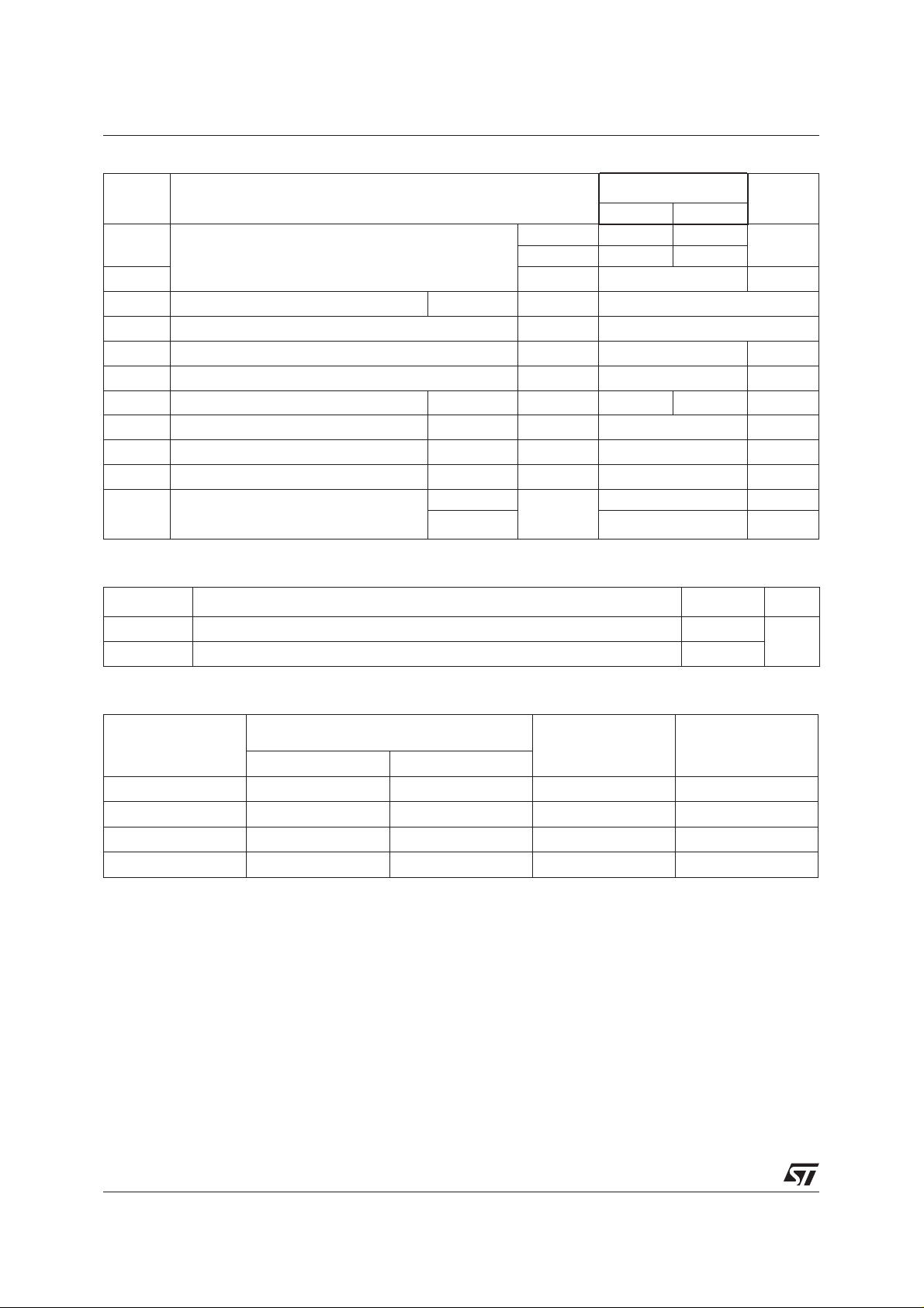
ABSOLUTE RATINGS (l imiting values)
Symbol Parameter Value Unit
I
T(RMS)
IT
(AV)
I
TSM
²
I
dI/dt
I
GM
P
G(AV)
T
stg
Tj
RMS on-state current (180° conduction angle) Tl = 60°C 4 A
Tamb = 25°C 1.35
Average on-state current ( 1 80° conduction angle) Tl = 60°C 2.5 A
Tamb = 25°C 0.9
Non repetitivesurgepeak on-state
current
tI
²
t Value for fusing
Critical rate of rise of on-state current
I
=2xIGT,tr≤100ns
G
Peak gate current tp = 20 µs Tj = 125°C 1.2 A
Average gate power dissipation Tj = 125°C 0.2 W
Storage junction temperature range
Operating junction temperature range
tp = 8.3 ms
Tj = 25°C
tp = 10 ms 30
tp = 10 ms Tj = 25°C 4.5
F = 60 Hz Tj = 125°C 50 A/µs
- 40to+150
-40to+125
33 A
2
A
S
°C
September 2000 - Ed: 3
1/5
X04 Series
ELECTRICAL CHARACTERISTICS (Tj = 25°C, unless otherwise specified)
Symbol Test Conditions X04xx Unit
02 05
I
GT
VD=12V RL=140Ω
V
GT
V
V
dV/dt
V
V
I
DRM
I
RRM
VD=V
GD
RG
I
H
I
L
TM
t0
R
d
DRMRL
IRG=10µA
I
=50mA RGK=1kΩ
T
IG=1mA RGK=1kΩ
=67%V
V
D
ITM=8A tp=380µs
Threshold voltage Tj = 125°C MAX. 0.95 V
Dynamic resistance Tj = 125°C MAX. 100 mΩ
V
DRM=VRRM
=3.3kΩ RGK=1kΩ
DRMRGK
THERMAL RESISTANCES
=1kΩ
RGK=1kΩ
Tj = 125°C MIN.
Tj = 110°C MIN. 10 15 V/µs
Tj = 25°C MAX. 1.8 V
Tj = 25°C MAX. 5 µA
Tj = 125°C 1 mA
MIN. _ 20
MAX. 200 50
MAX. 0.8 V
0.1 V
MIN.
8V
MAX. 5 mA
MIN. 6 mA
µA
Symbol Parameter Value Unit
R
R
th(j-a)
th(j-l)
Junction to leads (DC)
Junction to ambient (DC)
15
100
PRODUCT SELECTOR
Part Number
Sensitivity
600 V 800 V
X0402MF X 200 µA TO202-3
X0402NF X 200 µA TO202-3
X0405MF X 50 µA TO202-3
X0405NF X 50 µA TO202-3
Voltage
Package
°C/W
2/5

X04 Series
ORDERING INFORMATION
OTHER INFORMATION
Part Number Marking Weight Base Quantity Packing mode
X04xxyF 1AA2 X04xxyF 0.8 g 250 Bulk
X04xxyF 0AA2 X04xxyF 0.8 g 50 Tube
Note:xx = sensitivity, y = voltage
Fig. 1: Maximum average power dissipation
versus average on-state current.
Fig. 2-2: Average and D.C. on-state current
versus ambient temperature (device mounted on
FR4 with recommended pad layout).
Fig. 2-1: Average and D.C. on-state current
versus lead temperature.
Fig. 3: Relative variation of therm al impedance
junction to ambient versus pulse duration.
3/5

X04 Series
Fig. 4: Relative variation of gate trigger current,
holding current and l atching current versus
junction temperature (typical values).
Fig. 6: Relative variation of dV/dt immunity
versus gate-cathode resistance (typical values).
Fig. 5: Relative variation of holding current
versus gat e-cathode resistance (typical values).
Fig. 7: Relative variation of dV/dt immunity
versus gate-cathod e capacitance (typical
values).
Fig. 8: Surge peak on-state current versus
number of cycles.
4/5
Fig. 9: Non-repetitive surge pea k on-state
current for a sinusoidal pulse with width
tp < 10 ms, and corresponding value of I²t.

Fig. 10: On-state characteristics (maximum
values).
PACKAGE MECHANICAL DATA
TO202-3 (Plastic)
X04 Series
DIMENSIONS
REF.
Millimeters Inches
Min. Typ. Max. Min. Typ. Max.
A 10.1 0.398
C 7.3 0.287
D10.5 0.413
F1.50.059
H0.51 0.020
J 1.5 0.059
M 4.5 0.177
N5.30.209
N1 2.54 0.100
O1.40.055
P0.70.028
Information furnished is believed to be accurate and reliable. However, STMicroelectronics assumes no responsibility for the consequences
ofuse ofsuchinformation nor for anyinfringementofpatentsor otherrightsofthirdpartieswhich may result fromitsuse.No license isgranted
by implication or otherwise under anypatent or patent rights ofSTMicroelectronics. Specifications mentioned in this publication are subject
to change withoutnotice. Thispublicationsupersedes and replaces allinformationpreviously supplied.STMicroelectronics products arenot
authorized for use as critical components in life support devices or systems without express written approval of STMicroelectronics.
© TheSTlogo is aregistered trademark ofSTMicroelectronics
© 2000 STMicroelectronics - Printed in Italy - All Rights Reserved
STMicroelectronics GROUP OF COMPANIES
Australia - Brazil - China - Finland - France - Germany - Hong Kong - India - Italy - Japan - Malaysia - Malta - Morocco
Singapore - Spain- Sweden - Switzerland - UnitedKingdom
http://www.st.com
5/5
 Loading...