

查询VS6552供应商
VS6552
VGA Color CMOS Image Sensor Module
FEATURES
■ Small physical size
■ Ultra low power standby mode
■ SmOP (Small Optical Package) technology
featuring integrated lens
■ Class leading low light performance
■ VGA resolution sensor
■ Compatible with STV0974 companion mobile
processor
■ High frame rate to minimize image distortion
■ Low EMI link (VisionLink) to STV0974
■ On-chip 10-bit ADC
■ Automatic dark calibr ati on
2
■ I
C communications
■ On-chip PLL
DESCRIPTION
The VS6552 is a VGA resolution SmOP sensor
module. SmOP technology combines the image
sensor and fixed focus lens system in a single
module. This approa ch provides a nu mber of advantages:
– SmOP technology is suitable for high volume
manufacturing
– S mOP can be plugged into a PCB mounted
flow soldered socket
– SmOP can be mounted close to noisy RF
source as differential signalling used to
transmit data has good immunity from radio
interference.
The sensor outputs raw Bayer colorized data to
the STV0974 companion mobile processor.
STV0974 then perf orms all color processi ng and
exposure control functions before outputting the
data in an appropriate interface format like YCbCr,
RGB or JPEG.
VS6552 offers an ul tra low power standby mode
that consumes less than 15 µW.
The SmOP lens has been designed to combine
class leading low light performance with good
depth of field to ensure excellent overall optical
performance. The lens is a 2 element moulded
plastic design.
The output data an d qualificatio n clock are transmitted over low noi se, low v oltag e and fu lly d ifferential links. VS6552 configuration registers are
controlled via a private I
2
C interface to STV0974.
APPLICATIONS
■ Mobile phone embedded camera system
■ PDA embedded camera or accessory camera
■ Wireless security camera
Table 1. Technical Specifications
Pixel resolution 644 x 484 (VGA)
Pixel size 5.6µm x 5.6µm
Exposure control +81 dB
Analog gain +24 dB (max)
Dynamic range 60 dB (Typical)
Signal to noise at
2
50cd.m
Supply voltage
Power consumption
Package size
Lens
Package type 14 pad SmOP
37 dB (Typical)
2.8 V (analog supply)
1.8 V (digital supply)
<75 mW (@30 frame/s)
<15 µW (standby mode)
10.7mm x 8.7mm x
6mm:SmOP1.5
9.5mm x 8.5mm x 6.1mm
:SmOP2
o
HFOV, f# 2.8
45
System attach Socket or flexible circuit
Rev. 2
1/26October 2004

VS6552
Table 2. Order Codes
Part Number
VS6552V015/T 2 [ -25; +55 ] °C SmOP1.5
VS6552V02C/T 2 [ -25; +55 ] °C SmOP2M
VS6552V02D/T 2 [ -25; +55 ] °C SmOP2ME
Operating
Temperature
Package
2/26

VS6552
TABLE OF CONTENT
Overview ........................................................................................................................................... 4
Sensor Overview 4
Signal Description ........................................................................................................................... 5
Functional Description .................................................................................................................... 6
Analog Video Block 6
Digital Video Block 6
Device Operating Modes 7
Power Management 7
Clock and Frame Rate Timing 8
Control and Video Interface Formats 9
Electrical Characteristics ................................................................................................................ 9
DC Electrical Characteristics 10
AC Electrical Characteristics 10
ESD Handling Characteristics 13
Optical specification...................................................................................................................... 13
Defect Categorization .................................................................................................................... 13
Pixel Defects 13
Package Mechanical Data ............................................................................................................. 13
SmOP1.5 Module Outline 13
SmOP2 M Module Outline 13
SmOP2 ME Module Outline 13
Application Information................................................................................................................. 23
Socket 23
EMC and Shielding 23
Revision History............................................................................................................................. 25
3/26
VS6552
1 OVERVIEW
1.1 Sensor Overview
The VS6552 VGA image sensor produces raw
VGA digital video data at up to 30 frames per second. The image data is digit ized using an internal
10-bit column ADC. The resulting 10-bit output
data includes embe dded codes for synchronization. The data is formatted and transmi tted over a
fully differential link. The data is accompanied by a
qualifying clock th at is transmitted ov er an identical fully differential link .
The sensor is ful ly config urab le us ing an I
2
C inter-
face.
The sensor is optimized for high volume mobile
applications
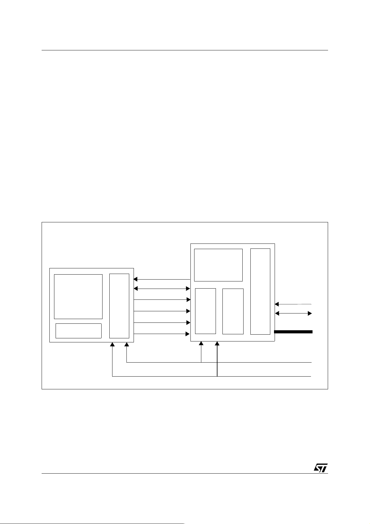
1.1.1 Typical Application - Mobile Application
Figure 1. Camera System Using STV0974
The VS6552 is an image sensor, it should be used
in conjunction with the STMicroelectronics
STV0974 companion processor. The coprocessor
and the sensor together form a complete im aging
system.
The sensors main function is to convert the viewed
scene into a data stream. The companion processor function is to manage the sensor so that it can
produce the best possible data and to process the
data stream into a form which is easily handled by
up stream mobile baseband or MMP chipsets.
The sensor supplies high speed clock signal to the
processor and provides the embedded control sequences which allow the co processor to synchronize with the frame and line level timings. The
processor then performs the color processing on
the raw image data from the sensor before supplying the final image data to the host.
STV0974
VS6552
Pixel
Array
ADC
Microprocessor
MSCL
MSDA
PCLKP
PCLKN
Digital Logic
PDATAP
PDATAN
VP
VC
Interface Logic
SCL
SDA
DIO[0:13]
CLK
PDN
4/26

2 SIGNAL DESCRIPTION
Table 3. Signal Description
Pad Number Pad Name I/O Type Description
Power supplies
VS6552
System
Control
Data
1CEXT PWR
Connection to capacitor
a
2 AGND PWR Analog ground
3 AVDD PWR Analog power
8 GND PWR Digital ground
11 VDD PWR Digital power
4PDN I
Power down control
b
5 CLK I System clock input
6 MSCL I Serial communication clock
7 MSDA I/O Serial communication data
9 PCLKN vLVDS output Output qualifying clock
10 PCLKP vLVDS output Output qualifying clock
12 PDATAN vLVDS output Serial output data
13 PDATAP vLVDS output Serial output data
Not connected
14 Not connected
NC Not connected
a.Internally generated v oltage that needs to be externally decoupled with a 100 nF, 5 V capacitor
b.Signal is active low
Note: The physical position of t he sign als on the pa ckag e can be found by referi ng t o th e pino ut inf ormat ion in Chapter7: Package Mechan-
ical Data.
5/26
VS6552
3 FUNCTIONAL DESCRIPTION
The first sections of this chapter detail the main
blocks in the device:
■ Analog video block
■ Digital video block
The later sections of th is chapter describe other
functional aspects of the de vice. Devic e level op erating modes, including suspend, are detailed
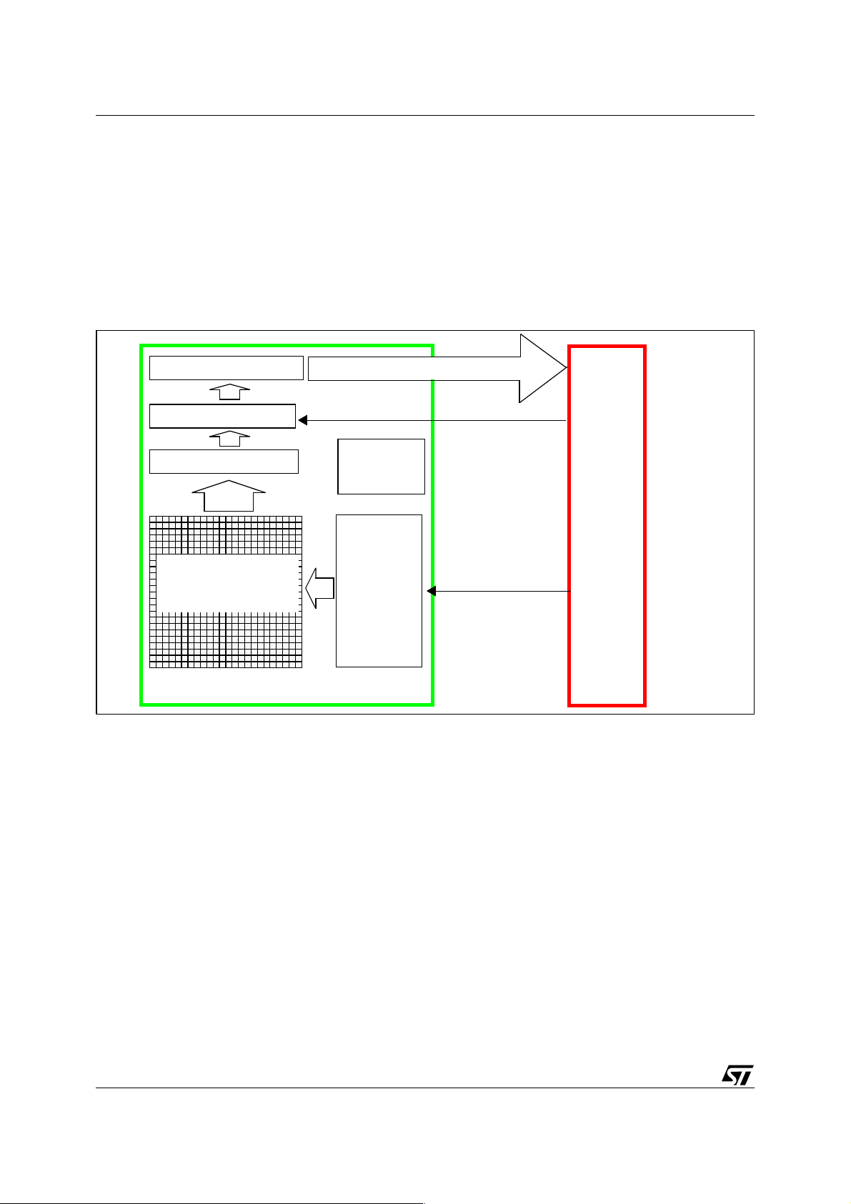
Figure 2. Analog Video Block
SRAM readout
X-Address
Column ADC
raw sensor data
Power
management
3.1 Analog Video Block
3.1.1 Features
■ ADC: 10-bit A/D converter - SRAM readout
■ Dynamic range 60 dB (typical)
■ SNR 37 dB @ 50 cd.m
2
(typical)
Timing signals
Digital
logic
VGA
pixel
array
3.1.2 Analogue Block Diagram
The analog video block f rom Figure 4, consis ts of
a VGA resolution pi xel a rray, p ower m anagem ent
circuitry. The digi tal block provides all timing signals to drive the analog block.
Pixel voltage values are read out and digitized using the address decoders and column ADC
3.2 Digital Video Block
3.2.1 Features
■ Frame rate: 30 frame/s max. (VGA) can be
reduced down to less than 3 frame/s (VGA)
■ Automatic dark calibration to ensure consistent
video level over varying scenes
Y address
Timing signals
■ Fixed pattern noise (FPN) data gathering
■ Line and frame statistics gathering
■ On-chip Power-On-Reset cell
■ Single video output format: VGA 640 x 480
■ H - Scaler function to aid software only
viewfinder implementations
3.2.2 Dark Calibration Algorithm
VS6552 runs a dark calibrati on algorithm on the
raw image data to control the video offsets caused
by dark current. This en sures that a high quality
image is output over a rang e of operating conditions. First frame dark level is corre ctl y cal ibrat ed,
for subsequent frames the a djust ment o f the d ark
level is damped by a leaky integrator function to
avoid possible frame to frame flicker.
6/26
VS6552
3.2.3 Image Statistics
VS6552 generates image s tatistics which can be
used by STV0974 as an input to an auto exposure
controller (AEC), a utomatic gain controller (AGC )
and automatic white balance (AWB). .
3.3 Device Operating Modes
3.3.1 Standby
This is the lowest power consumption mode. I
2
communications to STV 097 4 a re not supported in
this mode. The clock input pad, PLL and the video
blocks are powered down.
3.3.2 Sleep Mode
2
Sleep mode preserves the contents of the I
ister map. I
2
C communications to STV0974 are
C reg-
supported in this mode. The sleep mode is selected via a serial interface command sent by
STV0974. The data pads go high at the end of the
current frame. At this point the video block and
Table 4. VS6552 Power-up Sequence
Design block powered down
Mode
I2C Digital
PLL & CLK
pins
PLL power down. The internal video timing is reset
to the start of a video frame in prepara tion for the
enabling of active vide o. The values of the serial
interface registers like exposure and gain are preserved. The system clock must remain active to allow communication with the sensor.
3.3.3 Clock Active Mode
This mode is sim ilar to ‘sleep mode’ except t hat
the PLL is now powered up to permit a PCLKP/
PCLKN signal to be delivered to STV0974. The
C
PDATAP/PDATAN pads remain in ac tive. The vid eo block is powered down.
3.3.4 Idle Mode
VCAP is generated. The analog video block is now
powered up but the array is he ld in rese t and the
output PDATAP/PDATAN pads remain high.
3.3.5 Video
The VS6552 streams live video to the STV0974.
Video data
a b
Output pins Analog
inhibit
Standby
(PDN low)
Sleep No Yes Yes Yes Yes Yes
Clock
active
Idle No No No No No Yes
Video
a.PLL (Phase Locked Loop) generates fast system clock for STV0974
b.PLL, PCLKP and PCLKN pins
3.4 Power Management
VS6552 requires a dual power supply. The analog
circuits are powered by a nominal 2.8 V supply
Yes Yes Yes Yes Yes Yes
No No No Yes Yes Yes
No No No No No No
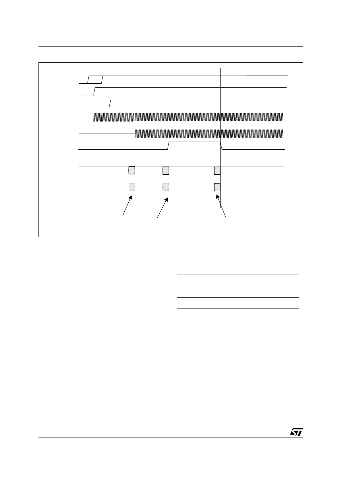
3.4.1 Power-up, Power-down Procedures
The power up and power down procedures are de-
tailed in the following Figure 3.
while the digital logic and digi tal I/O are powered
by a nominal 1.8 V supply.
7/26
VS6552
Figure 3. VS6552 Power-up Sequence
VDD (1.8V)
AVDD (2.8V)
PDN
CLK
PCLKP/N
PDATAP/N
MSDA
MSCL
Mode Change: Sleep -> Clock active Mode Command: Idle -> Streaming
and enable data qualification clock and
Standby Idle
general configuration
Sleep Streaming
Clock active
Mode Change: Clock active -> Idle
also enable data output
3.4.2 Active Signals with Unpowered VS6552
All signals going into the VS6552 must be either at
a low state or high impe dance when powe r is removed from the device. The exceptions to this rule
are the I
2
C lines which may be at a low or high
state and the clock which can be active.
3.5 Clock and Frame Rate Timing
3.5.1 Video Frame Rate Control
The output frame rate of VS6552 c an be reduced
by extending the frame length. The extension is
achieved by adding 'blank' video lines to act as
timing padding. This is advantageous as it does
not reduce the pixel readout rate and therefore
does not introduce unwanted motion distribution
effects to the image. The frame rate can be reduced from the default 3 0 fram e/s at VG A res olution to less than 3 frame/s at VGA resolution.
3.5.2 PLL and Clock Input
A PLL IP block is embedded. This block generates
all necessary int ernal clocks from an inp ut range
defined in Table 5. The input clock pad accepts up
to 26 MHz signals.
Table 5. System Input Clock Frequency Range
System clock frequency
Min. (MHz) Max. (MHz)
6.5 26
a.The standard su ppor ted i nput fre quenci es (i n MHz) are as
follows: 6.5, 8.4, 9, 9.6, 9.72, 12,13, 16.8, 18, 19.2,
19.44, 26.
a
3.5.3 Clock Input Type
VS6552 can receive the following clock types:
■ Single ended CMOS
■ Single ended Sine wave
■ Clock can be AC or DC coupled
The clock is fail-safe.
8/26

VS6552
3.6 Control and Video Interface Formats
The transmission line pairs and custom transmit -
ters/receivers realize a very low voltage differential
3.6.1 Overview
Data is transferred from VS6552 to STV0974 via a
high spee d serial link (VisionLink). The serial data
link comprises of two pairs of wires. The serial
control data is transferred between the VS6552 to
STV0974 via a private I
2
C bus.
3.6.2 VisionLink Physical Layer
Data signals (PDATAP and PD ATAN) and clock
signals (PCLKP and PCLKN) are transferred from
VS6552 to STV0974 via 2 pairs of balanced 100 Ω
(vLVDS) signalling scheme that can transfer infor-
mation in a potent ially noisy envi ronment. As im-
plemented in VS6552, VisionLink supports the
transmission of raw Bayer data at VGA resolution
up to 30 frame/s.
3.6.3 Serial I2C Control Bus
The internal registers in VS6552 can be config-
ured by STV0974 via a priv ate I
2
C bus. STV0974
is the bus maste r and VS6552 is the single slave.
VS6552 sends and r eceives co mmands ove r this
bus at up to 400 kHz.
impedance transmission lines.
4 ELECTRICAL CHARACTERISTICS
Table 6. Absolute Maximum Ratings
Symbol Parameter Values Unit
VDIG Digital power supply -0.5 to 3.0 V
VANA Analog power supply -0.5 to 3.6 V
MSCL,
MSDA
PDN, CLK Power Down Control, System Clock Input -0.3 to VDIG + 0.3 V
T
STO
Note: Caution: Stresses abov e those l isted und er “Absolute Maximum Rati ngs” may caus e permanent da mage to the device. This is a stres s
rating only and funct i onal operation of the device at these or any other conditions above those indicated in the operational sections of
the specification is not implied . Exposure to absolute maximum rating conditions for extended periods may affect device reliability.
CCI Signals -0.3 to VDIG + 0.3 V
Storage temperature -40 to + 85
o
C
Table 7. Operating Conditions
Symbol ParTyp.ameter Min. Typ. Max. Unit
Voltag e
V
DD
AV
DD
Tem per atur e
T
AF
T
AN
T
AO
Note: 1. Storage temperature: Camera has no permanent degradation
2. Functional operating temperature: Camera is electrically functional
3. Normal operating temperature: Camera produces ‘acceptable’ images
4. Optimum performance temperature: Camera produces optimal optical performance
Digital power supply voltage 1.7 - 1.9 V
Analog power supply voltage 2.5 - 3.3 V
Temperature (functional operating) -30 - +70 °C
Temperature (normal operating) -25 - +55 °C
Temperature (optimal operating) +5 - +30 °C
9/26

VS6552
4.1 DC Electrical Characteristics
Note: Typical values quoted for nominal voltage and temperature. Maximum values quoted for worse case operating conditions unless oth-
erwise specified.
Table 8. Power Supply VDIG, VANA
Parameter
Typ . M ax. Ty p. Max . U n it
Digital Analogue
Standby 1 5
NM
a
<2 µA
Video, 30fps 15 20 9 15 mA
a.Not Measurable - current is below the minimum calibrated measurement capabilities of the test system (1µA)
Table 9. System Clock
Symbol Parameter Min. Typ. Max. Unit
Leakage current
a.With DC coupled square wave clock
b.With DC 1V9 signal level applied
a
8
29
b
Table 10. I2C Interface - MSDA, MSCL
Symbol Parameter description Min. Typ. Max. Unit
V
IL
V
IH
V
OL
I
IL
I
IH
Low level input voltage - 0.3 VDIG V
High level input voltage
Low level output voltage
0.7 VDIG
b,c
a
-V
- 0.2 VDIG V
Low level input current - -10 µA
High level input current - 10 µA
µA
f Operating frequency range 0 -
a.For positive electros tat ic di scharges above 50 0V, a shift of VIH may happen. However, the device remains fully fu ncti onal ev en
for a stress up to 2000 V included, and VIH<0.9 V
age.
b.VOH not valid for CCI
c.1 mA drive strength
d.For external clock frequencies <19.2MHz Max limit is 200KHz
. Refer to the STV0974 datas heet for recommendations on MSCL/MSDA us-
DIG
400
d
4.2 AC Electrical Characteristics
Table 11. System Clock
Symbol Parameter description Min. Typ. Max. Unit
V
CL
V
CH
V
CAC
10/26
DC coupled square wave (low level) - 0.3 VDIG V
DC coupled square wave (high level) 0.7 VDIG V
AC coupled sine wave
a
0.5 1.0 1.2 V
kHz

Symbol Parameter description Min. Typ. Max. Unit
VS6552
f
CLK
a.Nominal frequencies are 6. 5 to 26MHz with a 1% center frequency tolerance
Clock frequency input
a
6.5 - 1%
a
-
Table 12. Timing Characteristics
Symbol Parameter description Min. Max. Unit
t
MSCL
t
LOW
t
HIGH
t
SP
t
BUF
t
HD.STA
t
SU.STA
t
HD.DAT
t
SU.DAT
t
R
MSCL clock frequency 0 400 kHz
Clock pulse width low 1.3 µs
Clock pulse width high 0.6 µs
Pulse width of spikes which are suppressed
by the input filter
050ns
Bus free time between transmissions 1.3 µs
Start hold tim e 0.6 µs
Start set-up time 0.6 µs
Data in hold time 0 0.9 µs
Data in set-up time 10 0 ns
MSCL/MSDA rise time
20+0.1C
a
b
300 ns
26 + 1%
b
MHz
t
F
t
SU.STO
MSCL/MSDA fall time
Stop set-up time 0. 6 µs
20+0.1 C
b
300 ns
Ci/o Input / Output capacitance (MSDA) 8 pF
Cin Input capacitance (MSCL) 6 pF
a.Cb = total capacitance on the lines
Figure 4. CCI AC characteristics
stopstartstop start
MSDA
MSCL
t
BUF
t
HD.STA
t
LOW
t
R
t
HD.DAT
t
HIGH
t
F
t
SU.DAT
...
t
HD.STA
...
t
SU.STAtSU.STO
Note: The VS6552 maximum I2C frequency of 400 kHz is only valid for external clock frequencies at or above 19.2 MHz. Due to a design
issue, for external clock frequencies below 19.2MHz, the maximum guaranteed I2C frequency is limited to 200 kHz.
11/26

VS6552
Table 13. vLVDS Interface AC Electrical Characteristics
Symbol Parameter description Min. Typ. Max. Unit
V
od
V
cm
R
O
I
DR
Differential voltage swing
Common mode voltage (self biasing) 0.8 0.9 1.0 V
Output Impedance 40 140 W
Drive current range (internally set by bias
circuit)
a,b
100 150 200 mV
0.5 1.5 2 mA
a.Supplies of VDIG = 1.8V and VANA = 2.8 V, Temperature = 25 °C
b.Measured over a 100 Ohm load
Table 14. vLVDS TIming Characteristics
Symbol Parameter Min. Typ. Max. Unit
f
PCLKP/
PCLKN
t
PCLKP/
PCLKN
t
LOW
t
HIGH
t
RISE
PCLKP/PCLKN clo ck freque nc y - - 120 MHz
PCLKP/PCLKN clo ck per iod 8.3 - 10 0 ns
PCLKP/PCLKN du ty cyc le 26 - 74 %
Low period of PCLKP/PCLKN 1.66 - ns
High period of PCLKP/PCLKN 1.66 - ns
Rise time of PDATAP/PDATAN, PCLKP/
PCLKN
0.3 - 0.5 ns
t
FALL
t
HD;DAT
t
SU;DAT
Fall time of PDATAP/PDATAN, PCLKP/
PCLKN
Data hold time 3 - - ns
Data set-up time 1 - - ns
Figure 5. VisionLink AC timing
PCLKP/
PCLKN
t
LOW
PDAT AP/
PDAT AN
t
SU;DAT
t
PCLKP/PCLKN
t
RISE
t
HIGH
0.3 - 0.5 ns
V
/2
DIG
t
FALL
V
/ 2
DIG
t
HD;DAT
12/26

VS6552
4.3 ESD Handling Characteristics
Table 15. ESD Handling Limits
Test Method Criteria
ESD Human
Body Model
ESD Machine
Model
Latch Up JESD78
JESD22 A114A
JESD22 A115A 200V
1.5 * Vddmax,
150mA
2kV
5 OPTICAL SPECIFICATION
The small amount of l ens relative illumina tion effects (field darkening) is corrected by the
STV0974.
Table 16. Optical Specifications
Parameter Value
Effective Focal Length 4 mm ± 0.15 mm
Aperture F2.8 apertu re
o
Horizontal Field of View
TV Distortion
(pin,cushion & barrel)
o
± 2
45
-3% to 3%
6 DEFECT CATEGORIZATION
6.1 Pixel Defects
A packaged CMOS image sensor will display visual imperfections caused either by electrical faults
or optical blemishes which can be introduced in
the product at various stages of the manufacturing
process. These imp urities can result in pixel de fects, that is a pi xel wh ose o utp ut is no t co nsis ten t
with the level of incide nt light fal ling on the image
sensor. The ability to identify and correct these defects is central to both the design requirements
and quality certifi cation, via test of STMicroelec tronics sensor products.
The STMicroelectronics STV0974 co-processor
implements defect correction algorithms which
screens the presence of the se defects in th e final
images. The defect cor rection algorithms ensure
that the VS6552 sensor in conjunction with the
STV0974 co-processor will produce a high quality
final image.
7 PACKAGE MECHANICAL DATA
7.1 SmOP1.5 Module Outline
– Figure 7
– Figure 8
– Figure 9
Figure 6.
MTF (
@ 60 cm @ 45 cycle/mm
)
– On axis: 45 %
– Horizontal field: 30%
– Diagonal field: 30%
Figure 6. MTF Points on the Image Field
on axis
horizontal
field
diagonal
field
7.2 SmOP2 M Module Outline
– Figure 10
– Figure 11
– Figure 12
7.3 SmOP2 ME Module Outline
– Figure 13
– Figure 14
– Figure 15
13/26

VS6552
Figure 7. SmOP1.5 Module Outline
ECN No.
Revision note Date Checked
B See Sheet 2 for details 19/01/04
RevNo
10.56 ±0.06
8.25
8.56
Note 9
Note 13
0.60 ±0.03
7.25
0.80
0.40
3.55 MAX
B
3.26
8.26
4.33
1.40
0.87
1.90 ±0.15
0.15 ±0.03
5.80 ±0.22
Scale
1 of 3
Sheet
3.05 ±0.19
Do Not Scale
SmOP 1.5, Ver 2.22 Low
0.06 B
4.58 ±0.085.42 ±0.08
CL Lensholder
All dimensions
Profile Camera Outline
STMicroelectronics
Title
in mm
Consumer & Micro Group - Imaging Division
7526498
Part No.
5.70 ±0.035
0.00 0.15
CL Ceramic
Sig. Date
Note 9
1.50 TYP
A
C
Drawn
Checked
Appd. Mech.
Appd. Elect.
Appd. Prod.
3.90 ±0.22
Note 10
Appd. Q.A.
3°
8.66 ±0.06
0.00 0.15
4.05 ±0.084.05 ±0.08
CL Lensholder
14/26
draft
3°
Finish
Material
CL Ceramic
Note 10
±0.05
0.10
R
0.75
15°
Gate Position
C (20 : 1)
B
All dimensions in mm
This drawing is the property of STMicroelectronics
and will not be copied or loaned without the
Interpret drawing per BS308, 3RD Angle Projection
written permission of STMicroelectronics.
0.25
Linear
0 Place Decimals 0 ±1.0
1 Place Decimals 0.0 ±0.10
2 Place Decimals 0.00 ±0.07
Angular ±0.25 degrees
Diameter +0.10/-0.00
Position 0.10
Notes:
1. Mass of module 0.50 grammes
2. Volume of Module 278 mm^3
3. 2 max draft angle on all moulded components unless
otherwise stated.
4. Surface finish on external moulded surfaces is RA 16
(Charmille 24).
5. Surface finish on base of ceramic is TBD.
6. All gates on moulded parts will be sub flush.
7. All mouldings to be free from visible flash or mismatch.
8. Uniformly distributed load of 20N may be applied to datum
surfaces A & B.
9. These numbers denote tool No. and cavity.
10. Edge of ceramic and glue bead will not protrude past edge
of lensholder.
11. Dimensions enclosed thus are inspection dimensions.
12. Minimum breaking torque between lensholder and barrel is
40 Nmm.
13. These 3 depressions contain gates or are used for cavity &
tool identification and ejector pin locations.
Tolerances, unless otherwise stated
Surface Finish 1.6 microns

Figure 8. SmOP1.5 Module Outline
Makrolon: 2405
Makrolon: 2405
Colour Black
max.
39°
(Pyramid)
Colour Black
COP: Zeonex E48R
COP: Zeonex E48R
E Glass Coated with
IR Filter Material
Silicon
Ceramic: Alumina
Dark Grey
max.
D-D (8 : 1)
3.36
At Datum B (Cone)
Top of image
VS6552
2 of 3
Sheet
Scale
Datum B (Pyramid)
2.69 max. at
D
Do Not Scale
SmOP 1.5, Ver 2.22 Low
Profile Camera Outline
Title
STMicroelectronics
All dimensions
in mm
Consumer & Micro Group - Imaging Division
7526498
Checked
Date
ECN No.
B
Note 10
, Now 61 17/02/04
1.4 min.
E
E (16 : 1)
Part No.
D
(cone)
61°
max.
B2
B
max.
(Pyramid)
50°
2.01 max. at
Datum B (Pyramid)
Sig. Date
Drawn
Checked
Appd. Mech.
Appd. Elect.
Appd. Prod.
Appd. Q.A.
Sub flush gate posn
See Note 6
Finish
Material
All dimensions in mm
This drawing is the property of STMicroelectronics
and will not be copied or loaned without the
Interpret drawing per BS308, 3RD Angle Projection
written permission of STMicroelectronics.
Field of View Data.
Revision note
A First Release as 7526498. Previous version of camera was 7487715
Barrel flange increased. Diameter on lens holder increased. Laser
weld recesses moved and length was 1.60, 0.30 feature on pin 1 12/05/03
was 0.50
B Tolerance added. Pad 1 dimension changed from 0.5 to 0.3mm 19/01/04
Material changed from Noryl HB1525 to Makrolon 2405.
RevNo
B2 Exclusion Cone corrected was 60
Pyramid
holes must not protrude into the Pyramid.
Edges of circular holes in customer's equipment
must not intrude into the Cone. Edges of rectangular
Cone
Tolerances, unless otherwise stated
Linear
0 Place Decimals 0 ±1.0
1 Place Decimals 0.0 ±0.10
0.10
+0.10/-0.00
Position
Surface Finish 1.6 microns
2 Place Decimals 0.00 ±0.07
Angular ±0.25 degrees
Diameter
15/26

VS6552
Figure 9. SmOP1.5 Module Outline
Scale
Sheet
3 of 3
ECN No.
5.70 ±0.05
Revision note Date Checked
Pad material is 0.30 microns
B See Sht 2 19/01/04
RevNo
gold on 2 microns nickel
Part Marking in Hatched areas.
Refer to Spec TBD for details.
1.20 ±0.03 typ
7.10 ±0.05
5.35 ±0.05
4.05 ±0.05
2.65 ±0.05
0
2.90 ±0.05
1.50 ±0.05
Pad 1
Do Not Scale
SmOP 1.5, Ver 2.22 Low
Profile Camera Outline
STMicroelectronics
Title
All dimensions
in mm
Consumer & Micro Group - Imaging Division
7526498
Part No.
0
B
Sig. Date
0.30 ±0.03
Drawn
Checked
Appd. Mech.
Appd. Elect.
Appd. Prod.
Appd. Q.A.
2.65 ±0.03
1.00 ±0.03
Material
Finish
16/26
Underside of module showing connector and test pad layout.
0.48 ±0.22
5.60 ±0.05
7.00 ±0.05
8.40 ±0.05
4.20 ±0.05
2.80 ±0.05
1.40 ±0.05
0
2.35 ±0.03 typ
0.48 ±0.22
All dimensions in mm
This drawing is the property of STMicroelectronics
and will not be copied or loaned without the
Interpret drawing per BS308, 3RD Angle Projection
Linear
Tolerances, unless otherwise stated
written permission of STMicroelectronics.
0 Place Decimals 0 ±1.0
1 Place Decimals 0.0 ±0.10
2 Place Decimals 0.00 ±0.07
Angular ±0.25 degrees
Diameter +0.10/-0.00
Position 0.10
Surface Finish 1.6 microns

Figure 10. Module Outline (SmOP 2M)
VS6552
Initial
5.46
Note 9
Note 10
See Sheet 3
Revision note Date
B2
RevNo
These cavities may contain glue.
Gate Location
7.20
0.40
0.80
6.10 ±0.10
5
R
2.70 ±0.10
Scale
Do Not Scale
8.95
1 of 3
Sheet
SMOP2-M
OUTLINE DRAWING
Title
STMicroelectronicsSTMicroelectronics
All dimensions
in mm
Consumer & Micro Group - Imaging Division
2 TYP
DBS
18/06/03
Date
Drawn
0.50 At Datum A
A
7540020
Part No.
4.25
B
4.75
0.60
9.50 ±0.06
+0.1
R0.10 0
2.40
0.40
8.50 ±0.06
1.50°
C (20 : 1)
If no radii
8.22 at Datum B
R0.10
R0.10
10°
0.50
0.52
1.68 ±0.10
B
B (20 : 1)
0.50
Note 13
A (20 : 1)
Note 14
Notes:
1. Mass of module: <0.5 grammes.
2. Volume of module: 370.2 mm^3.
3. 2 deg max draft angle on all moulded components unless
otherwise stated.
4. Surface finish on all external moulded surfaces is
Charmille 30 MAX.
5. Surfaces shown in silver to be conductively plated.
See sheet 2 for plating information.
Finish
Material
A
6. All gates to be sub flush.
7. All mouldings to be free from flash or mismatch.
8. Uniformly distributed load of 20N to be applied to datum
surfaces A & B.
9. These numbers denote tool number and cavity.
Text will be subflush with surface.
10.These depressions may be used to indicate
lens type, tool number and cavity.
C
All dimensions in mm
This drawing is the property of STMicroelectronics
and will not be copied or loaned without the
Interpret drawing per BS308, 3RD Angle Projection
11.Dimensions enclosed thus are inspection dimensions.
12.Breaking torque between lens barrel and holder
> 20 Nmm.
All Dimensions
13.Corners of the substrate will not protrude past the
rectangular footprint of the lens holder.
14.Glue bead will not protrude past edge of substrate.
Tolerances, unless otherwise stated
written permission of STMicroelectronics.
0 Place Decimals 0 ±1.0
1 Place Decimals 0.0 ±0.10
2 Place Decimals 0.00 ±0.07
Angular ±0.5 degrees
Position 0.10
Surface Finish 1.6 microns
17/26

VS6552
Figure 11. SmOP2 Module Outline
Initial
Noryl: N110
Cone
See Table Dim A
See Sheet 3
Revision note Date
B2
RevNo
Noryl: N110
COP or PC
COP or PC
E Glass with IR
Pyramid
See Table Dim B
B
Silicon
Substrate:
Glass/epoxy
filter Material
pre-preg
Pyramid
At Datum B
See Table Dim D
SCALE 5 : 1
SECTION B-B
Dim C
Pyramid
See Table
Cone
At Datum B
See Table Dim E
Scale
Do Not Scale
2 of 3
Sheet
SMOP2-M
OUTLINE DRAWING
Title
STMicroelectronicsSTMicroelectronics
All dimensions
in mm
Consumer & Micro Group - Imaging Division
BB
At Datum B
See Table Dim F
MAX Exclusion Zones Dimensions
DBS
Drawn
18/06/03
Date
7540020
Part No.
Module A B C D E F
4 micron SVGA 64 53.12 41.1 4.15 3.32 2.49
5.6 micron VGA 61 50.36 39.06 4 3.2 2.4
Exclusion Zones.
Edges of circular holes in customer's equipment must not intrude into the cone.
Edges of rectangular holes must not prodrude into the pyramid.
Dimensions shown are maximums.
Note: If an upgrate path from 5.6 micron VGA to 4 micron SVGA is required then the 4 micron SVGA
data should be used.
5
These cavities
See Plating Notes 2 and 3
may contain glue.
120°
AA
this area.
Cosmetics not
guaranteed outside
Probe points to contact
120°
Scallops may contain
US weld marks.
Weld will not protrude
"Class A" Surface
(Top face of barrel)
past cylindrical surface.
inside dotted lines.
2.40
These surfaces
to be plated
+0.3
0.94 - 0.1
Finish
Material
B2
All dimensions in mm
SCALE 6 : 1
SECTION A-A
Plating Notes
1. 4 point probe to be used to check resistance of the metalisation.
2. Probe to must not contact the lens mount in the scalloped areas.
3. Probe to contact the cylindrical section of the lens mount between any 2 of the 3
equi-spaced points around the diameter.
4. Plating Options:
a.1 micron Copper, 0.1micron MIN Stainless Steel
b.1 micron Copper, 0.1micron MIN Nickel Chrome
c.1 micron Copper, 0.1micron MIN TBD
5. Resistance to be less than 1 ohm.
6. Contact force to be 2N.
This drawing is the property of STMicroelectronics
and will not be copied or loaned without the
Interpret drawing per BS308, 3RD Angle Projection
All Dimensions
Tolerances, unless otherwise stated
written permission of STMicroelectronics.
0 Place Decimals 0 ±1.0
1 Place Decimals 0.0 ±0.10
2 Place Decimals 0.00 ±0.07
Angular ±0.5 degrees
Position 0.10
Surface Finish 1.6 microns
18/26

Figure 12. SmOP2 Module Outline
VS6552
Initial
DBS
010404
Revision note Date
See ADCS Revision A for previous history
B
RevNo
DBS
DBS
110604
160604
Area For Test Pads,
Additional Tracking
& Part Marking
Sheet 2, Note 5, Contact resistance changed to 1 ohm.
Sheet 2, Note 3 reworded.
Step in chamfer added. Note 4 corrected.
Notes revised to remove TBD. Torque spec changed to
20Nmm. Inspection dimension moved.
Surface finish changed to Charmille 30 MAX.
B1
Sheet 3, Pad outline note added.
Top diameter re-defined.
0.10 TYP
B2
1 ±0.03 TYP
0.20 TYP
CLKN
CCP
CLKP
CCP
VDIG
DATAN
CCP
DATAP
CCP
DGND
Test
Test
Test
Test
6.10
3.85
2.75
CCISDA DGND
CCISCL
EXTCLK
DOWN
XSHUT
VANA
AGND
VCAP
1.10 ±0.03
2.20 ±0.03
3.30 ±0.03
4.40 ±0.03
5.50 ±0.03
6.60 ±0.03
Scale
Sheet
Do Not Scale
SMOP2-M
OUTLINE DRAWING
Title
STMicroelectronicsSTMicroelectronics
All dimensions
in mm
Consumer & Micro Group - Imaging Division
DBS
18/06/03
7540020
Date
Drawn
Part No.
Finish
Material
3 of 3
±0.03 TYP
Underside of module showing connector and test pad layout.
1.50
Pad 14
Area for test pads,
additional tracks
and part marking.
No conductive contact
or force allowed in this area.
Pad 1
Pad Material is 0.3
microns minimum
gold on 5 microns
minimum nickel.
B2
Note:
All dimensions in mm
This drawing is the property of STMicroelectronics
and will not be copied or loaned without the
Interpret drawing per BS308, 3RD Angle Projection
Minimum size shown for pad.
All Dimensions
Pad spacing will be maintained.
Actual pad outlines may be extended.
Refer to individual product substrate drawings.
Tolerances, unless otherwise stated
written permission of STMicroelectronics.
0 Place Decimals 0 ±1.0
1 Place Decimals 0.0 ±0.10
2 Place Decimals 0.00 ±0.07
Angular ±0.5 degrees
Position 0.10
Surface Finish 1.6 microns
19/26

VS6552
Figure 13. SmOP2 Module Outline
Initial
5.46
Note 9
Date
Note 10
See Sheet 3
0.30
Revision note
B4
RevNo
Note 13
7.20
0.40
0.80
5
R
0.50 TYP
2.70 ±0.10
Scale
Do Not Scale
8.95
1 of 3
Sheet
SMOP2-ME
OUTLINE DRAWING
6.10 ±0.10
STMicroelectronicsSTMicroelectronics
Title
All dimensions
in mm
Consumer & Micro Group - Imaging Division
2 TYP
DBS
30/06/03
Date
7545055
Part No.
B
4.75
(7.30)
9.50 ±0.06
14 ±0.15
+0.10
R0.10 0
2.40
Drawn
0.50 at datum A
A
0.40
4.25
8 ±0.15
8.50 ±0.06
1.50°
Gate Location
R0.10
R0.10
0.50
C (20 : 1)
0.52
1.68 ±0.10
If no radii
8.22 at datum B
B
Finish
Material
A
C
0.50
B (20 : 1)
A (20 : 1)
Note 14
Notes:
1. Mass of module: <0.5 grammes.
2. Volume of module: 384.7 mm^3.
3. 2 deg max draft angle on all moulded components unless
otherwise stated.
4. Surface finish on all external moulded surfaces is
Charmille 30 MAX.
5. Surfaces shown in silver to be conductively plated.
See sheet 2 for plating information.
6. All gates to be sub flush.
7. All mouldings to be free from flash or mismatch.
8. Uniformly distributed load of 20N to be applied to datum
surfaces A & B.
9. These numbers denote tool number and cavity.
Text will be subflush with surface.
10.These depressions may be used to indicate
lens type, tool number and cavity.
11.Dimensions enclosed thus are inspection dimensions.
12.Breaking torque between lens barrel and holder
> 20 Nmm.
All dimensions in mm
This drawing is the property of STMicroelectronics
and will not be copied or loaned without the
Interpret drawing per BS308, 3RD Angle Projection
All Dimensions
Tolerances, unless otherwise stated
13.All translational and rotational placement tolerances are included in this area.
14.Glue bead will not protrude past edge of Lens Holder.
written permission of STMicroelectronics.
0 Place Decimals 0 ±1.0
1 Place Decimals 0.0 ±0.10
2 Place Decimals 0.00 ±0.07
Angular ±0.5 degrees
Position 0.10
Surface Finish 1.6 microns
20/26

Figure 14. SmOP2 Module Outline
VS6552
Initial
Date
Noryl N110
Cone
See Table Dim A
See Sheet 3
Revision note
B4
RevNo
COP or PC
COP or PC
Noryl N110
Pyramid
See Table Dim B
B
Silicon
Substrate:
Glass/epoxy
E Glass with IR
filter Material
pre-preg
SCALE 5 : 1
SECTION B-B
Pyramid
Cone
Pyramid
At Datum B
See Table Dim D
Dim C
See Table
At Datum B
See Table Dim E
Scale
Do Not Scale
2 of 3
Sheet
SMOP2-ME
OUTLINE DRAWING
STMicroelectronicsSTMicroelectronics
Title
All dimensions
in mm
Consumer & Micro Group - Imaging Division
BB
At Datum B
See Table Dim F
DBS
Drawn
30/06/03
Date
Part No.
7545055
MAX Exclusion Zones Dimensions
Module A B C D E F
4 micron SVGA 64 53.12 41.1 4.15 3.32 2.49
5.6 micron VGA 61 50.36 39.06 4 3.2 2.4
Exclusion Zones.
Edges of circular holes in customer's equipment must not intrude into the cone.
Edges of rectangular holes must not prodrude into the pyramid.
Dimensions shown are maximums.
Note: If an upgrate path from 5.6 micron VGA to 4 micron SVGA is required then
the 4 micron SVGA data should be used.
5
These cavities
may contain glue.
See Plating Notes 2 and 3
120°
AA
"Class A" Surface
this area
Cosmetics not
guaranteed outside
120°
(Top face of barrel)
Probe point to contact
inside dotted lines.
2.40
These areas
Scallops may contain
US weld marks.
Weld will not protrude
past cylindrical surface.
+0.3
to be plated.
0.94 - 0.1
Finish
Material
B4
All dimensions in mm
SCALE 5 : 1
SECTION A-A
Plating Notes
1. 4 point probe to be used to check resistance of the metalisation.
2. Probe to must not contact the lens mount in the scalloped areas.
3. Probe to contact the cylindrical section of the lens mount between any 2 of the 3
equi-spaced points around the diameter.
4. Plating Options:
a.1 micron Copper, 0.1micron MIN Stainless Steel
b.1 micron Copper, 0.1micron MIN Nickel Chrome
c.1 micron Copper, 0.1micron MIN TBD
5. Resistance to be less than 1 ohm.
6. Contact force to be 2N.
This drawing is the property of STMicroelectronics
and will not be copied or loaned without the
Interpret drawing per BS308, 3RD Angle Projection
All Dimensions
Tolerances, unless otherwise stated
written permission of STMicroelectronics.
0 Place Decimals 0 ±1.0
1 Place Decimals 0.0 ±0.10
2 Place Decimals 0.00 ±0.07
Angular ±0.5 degrees
Position 0.10
Surface Finish 1.6 microns
21/26

VS6552
Figure 15. SmOP2 Module Outline
Initial
Date
Revision note
RevNo
DBS
DBS
DBS
DBS
DBS
±0.03
010404
230104
040504
110604
160604
12.10
Notes 4 and 10 corrected. Top edge radius changed from +0.05
to +0.1mm.
Released into ADCS
B
B1
Top diameter defined.
Sheet 2, Note 5, Contact resistance changed to 1 ohm.
Sheet 2, Note 3 reworded.
Notes updated to remove TBD. Torque now aet to 20Nmm.
Inspection dimension moved.
B2
Sheet 3, Pad outline note added.
B4
B3 Surface finish changed to charmille 30 MAX.
6.60 ±0.03
5.50 ±0.03
4.40 ±0.03
3.30 ±0.03
2.20
1.10 ±0.03
DA
CCIS
CCIS
CCP
DGND
0.20 TYP
CL
CLKN
EXT
CCP
CLK
CLKP
DOWN
XSHUT
VDIG
CCP
VANA
DATAN
6.10
AGND
CCP
DATAP
3.85
2.75
VCAP
DGND
Pad 1
Any force applied to
the topside of the substrate
should be balanced by a
counter force directly opposite
on the underside of the
Pad 14
1.50 ±0.03 TYP
1 ±0.03 TYP
Scale
Do Not Scale
STMicroelectronicsSTMicroelectronics
All dimensions
in mm
Consumer & Micro Group - Imaging Division
DBS
Drawn
30/06/03
Date
substrate and vice versa.
3 of 3
Sheet
SMOP2-ME
OUTLINE DRAWING
Title
7545055
Part No.
1.451.45
Area For Test Pads &
Additional Tracking.
Pad Material is 0.3
microns minimum
gold on 5 microns
minimum nickel.
Area for
Part Marking.
DGND
CLKN
CCP
CLKP
CCP
VDIG
DATAN
CCP
CCP
DGND
DATAP
Test
Test
Test
Test
Underside of module showing connector and test pad layout.
1 ±0.03 TYP
Pad 14
(Test Duplicate)
1.50 ±0.03 TYP
DA
CL
CCIS
CCIS
CLK
EXT
DOWN
VANA
AGND
VCAP
XSHUT
1.10
2.20
3.30
4.40
Pad 1
(Test Duplicate)
Area for
Part Marking.
5.50
6.60
B4
No Force
allowed in
this area
Note:
Minimum size shown for pad.
Pad spacing will be maintained.
Actual pad outlines may be extended.
Refer to individual product substrate drawings.
Finish
Material
All dimensions in mm
This drawing is the property of STMicroelectronics
and will not be copied or loaned without the
Interpret drawing per BS308, 3RD Angle Projection
All Dimensions
Tolerances, unless otherwise stated
written permission of STMicroelectronics.
0 Place Decimals 0 ±1.0
1 Place Decimals 0.0 ±0.10
2 Place Decimals 0.00 ±0.07
Angular ±0.5 degrees
Position 0.10
Surface Finish 1.6 microns
22/26

VS6552
8 APPLICATION INFORMATION
8.1 Socket
ST has developed a low-profile socket for the
SmOP 1.5 package, which is suitable for reflow
soldering and manual / automatic inser tion of the
camera module. The socket has been designed to
withstand mobile phone grade reliability tests
(temperature, shocks, vibration, salt mist).
Please contact ST for details on ST P/N XS0015.
See Figure 16 for rec ommended PCB l ayout and
mechanical footprint of the XS0015 socket.
8.2 EMC and Shielding
The VS6552 is a low noise device and is highly tolerant of high leve ls of ra dio fr equenc y (RF ) radia tion. However if this device is closely mounted to a
sensitive receiver it is recommended that the
VS6552 is shielded to prevent reducing the sensitivity or channel masking of the receiver.
Recommended maximum field strength: 1kV/m.
Maximum radiated power transferred from the
VS6552 into a GSM monopo le antenna mounted
15 mm away from the VS6552 has peaks of inter-
ference at around -90 dBm. This is dependen t on
system design and layout.
To minimized the coupling b etween the G SM antenna and the sensor the following guide lines
should be observed.
Camera should be positioned as far away from the
GSM antenna as possible. The distance between
the low frequency (below 1GHz) resonant antenna
elements and the camera should also be maximized.
The VS6552 and its associated decoupling capacitors should NOT be connected together using the
antenna reference ground. The ground connections in the sub circuit should be connected either:
■ by a dedicated ground trace network, that is
connected by a single point to the main ground
of the system
■ by an internal ground plane, which is entirely
covered and single point connec ted to a
protective ground.
The PCLKP and PCLKN lines can be filtered to reduce the induced noise.
The protective ground sh ould be flooded around
the sensor socket pads to reduce the radiation aperture in the protective ground plane.
23/26

VS6552
Figure 16. SmOP1.5 Socket Mechanical Data
03/11/03
7,3
10
1,5
1,1
RECOMMENDED SOLDER
1,4
FM
par: le:Mise à jour version
SMOP 1.5
SOCKET FOR CAMERA MODULE
Ensemble:
Pièce:
Modif:
Le:
-
Dessiné par:
Réf:
04/02/03
FM
24/26
11,7
10,5
VACUUM P&P
CLEARANCE FOR
5/1
Matière:
Echelle:
-
Tolérances
-
-
Générales:
Ra général:
Vérifié par:

9 REVISION HISTORY
Table 17. Revision History
Date Revision Description of Changes
May 2004 1 First Release of Product Preview
Second Release - Document status changed to datasheet. to reflect the
21 October 2004 2
product maturity level.
Changes applied in Electrical Characteristics and Package Information
with the addition of two packages (SmOP2M and SmOP2ME).
VS6552
25/26

VS6552
Information furnished is believed to be accurate and reliable. However, STMicroelectronics assumes no responsibility for the consequences
of use of such information nor for any infrin gement of patents or other rights of third parties which may resul t from its use. No license is granted
by implication or otherwise under any patent or patent rights of STMicroelectronics. Specifications mentioned in this publication are subject
to change without not ic e. This publication supersedes and replaces all information previously supplied. ST Microelectronics products are not
authorized for use as critical components in life support devices or systems without express writte n approval of STMicroelectronics.
The ST logo is a registered trademark of STMicroelectronics.
All other names are the property of their respective owners
© 2004 STMicroelectronics - All rights reserved
STMicroelectronics group of companies
Australia - Belgium - Brazil - Canada - China - Czech Republic - Finland - France - Germany - Hong Kong - India - Israe l - Italy - Japan -
Malaysia - Malta - Morocco - Singapore - Spain - Sweden - Switzerland - United Kingdom - United Stat es of America
www.st.com
26/26
 Loading...