

Features
VNS3NV04D-E
OMNIFET II
fully autoprotected Power MOSFET
Max On-State resistance (per ch.) R
Current limitation (typ) I
Drain-Source clamp voltage V
■ Linear current limitation
■ Thermal shut down
■ Short circuit protection
■ Integrated clamp
■ Low current drawn from input pin
■ Diagnostic feedback through input pin
■ Esd protection
■ Direct access to the gate of the power mosfet
LIMH
CLAMP
ON
120mΩ
3.5A
40V
(analog driving)
■ Compatible with standard power mosfet
SO-8
Description
The VNS3NV04D-E is a device formed by two
monolithic OMNIFET II chips housed in a
standard SO-8 package. The OMNIFET II are
designed in STMicroelectronics VIPower M0-3
Technology: they are intended for replacement of
standard Power MOSFETs from DC up to 50KHz
applications. Built in thermal shutdown, linear
current limitation and overvoltage clamp protects
the chip in harsh environments.
Fault feedback can be detected by monitoring the
voltage at the input pin.
Table 1. Device summary
Package
SO-8 VNS3NV04D-E VNS3NV04DTR-E
July 2007 Rev 2 1/21
Order codes
Tube Tape and Reel
www.st.com
21

Contents VNS3NV04D-E
Contents
1 Block diagram and pin description . . . . . . . . . . . . . . . . . . . . . . . . . . . . . 5
2 Electrical specifications . . . . . . . . . . . . . . . . . . . . . . . . . . . . . . . . . . . . . . 6
2.1 Absolute maximum ratings . . . . . . . . . . . . . . . . . . . . . . . . . . . . . . . . . . . . . 6
2.2 Thermal data . . . . . . . . . . . . . . . . . . . . . . . . . . . . . . . . . . . . . . . . . . . . . . . 7
2.3 Electrical characteristics . . . . . . . . . . . . . . . . . . . . . . . . . . . . . . . . . . . . . . . 7
2.4 Electrical characteristics curves . . . . . . . . . . . . . . . . . . . . . . . . . . . . . . . . 12
3 Protection features . . . . . . . . . . . . . . . . . . . . . . . . . . . . . . . . . . . . . . . . . 16
3.1 Overvoltage clamp protection . . . . . . . . . . . . . . . . . . . . . . . . . . . . . . . . . . 16
3.2 Linear current limiter circuit . . . . . . . . . . . . . . . . . . . . . . . . . . . . . . . . . . . 16
3.3 Overtemperature and short circuit protection . . . . . . . . . . . . . . . . . . . . . . 16
3.4 Status feedback . . . . . . . . . . . . . . . . . . . . . . . . . . . . . . . . . . . . . . . . . . . . 16
4 Package and packing information . . . . . . . . . . . . . . . . . . . . . . . . . . . . . 17
4.1 ECOPACK® packages . . . . . . . . . . . . . . . . . . . . . . . . . . . . . . . . . . . . . . . 17
4.2 SO-8 Package mechanical data . . . . . . . . . . . . . . . . . . . . . . . . . . . . . . . . 18
4.3 SO-8 Packing information . . . . . . . . . . . . . . . . . . . . . . . . . . . . . . . . . . . . . 19
5 Revision history . . . . . . . . . . . . . . . . . . . . . . . . . . . . . . . . . . . . . . . . . . . 20
2/21

VNS3NV04D-E List of tables
List of tables
Table 1. Device summary . . . . . . . . . . . . . . . . . . . . . . . . . . . . . . . . . . . . . . . . . . . . . . . . . . . . . . . . . . 1
Table 2. Absolute maximum ratings . . . . . . . . . . . . . . . . . . . . . . . . . . . . . . . . . . . . . . . . . . . . . . . . . . 6
Table 3. Thermal data. . . . . . . . . . . . . . . . . . . . . . . . . . . . . . . . . . . . . . . . . . . . . . . . . . . . . . . . . . . . . 7
Table 4. Off . . . . . . . . . . . . . . . . . . . . . . . . . . . . . . . . . . . . . . . . . . . . . . . . . . . . . . . . . . . . . . . . . . . . . 7
Table 5. On . . . . . . . . . . . . . . . . . . . . . . . . . . . . . . . . . . . . . . . . . . . . . . . . . . . . . . . . . . . . . . . . . . . . . 7
Table 6. Dynamic . . . . . . . . . . . . . . . . . . . . . . . . . . . . . . . . . . . . . . . . . . . . . . . . . . . . . . . . . . . . . . . . 8
Table 7. Switching . . . . . . . . . . . . . . . . . . . . . . . . . . . . . . . . . . . . . . . . . . . . . . . . . . . . . . . . . . . . . . . 8
Table 8. Source Drain diode . . . . . . . . . . . . . . . . . . . . . . . . . . . . . . . . . . . . . . . . . . . . . . . . . . . . . . . . 8
Table 9. Protections (-40°C < Tj < 150°C, unless otherwise specified) . . . . . . . . . . . . . . . . . . . . . . . 9
Table 10. Document revision history . . . . . . . . . . . . . . . . . . . . . . . . . . . . . . . . . . . . . . . . . . . . . . . . . 20
3/21

List of figures VNS3NV04D-E
List of figures
Figure 1. Block diagram . . . . . . . . . . . . . . . . . . . . . . . . . . . . . . . . . . . . . . . . . . . . . . . . . . . . . . . . . . . . 5
Figure 2. Configuration diagram (top view) . . . . . . . . . . . . . . . . . . . . . . . . . . . . . . . . . . . . . . . . . . . . . 5
Figure 3. Current and voltage conventions . . . . . . . . . . . . . . . . . . . . . . . . . . . . . . . . . . . . . . . . . . . . . 6
Figure 4. Switching time test circuit for resistive load . . . . . . . . . . . . . . . . . . . . . . . . . . . . . . . . . . . . . 9
Figure 5. Test circuit for diode recovery times . . . . . . . . . . . . . . . . . . . . . . . . . . . . . . . . . . . . . . . . . . 10
Figure 6. Unclamped inductive load test circuits . . . . . . . . . . . . . . . . . . . . . . . . . . . . . . . . . . . . . . . . 10
Figure 7. Input charge test circuit. . . . . . . . . . . . . . . . . . . . . . . . . . . . . . . . . . . . . . . . . . . . . . . . . . . . 11
Figure 8. Unclamped inductive waveforms . . . . . . . . . . . . . . . . . . . . . . . . . . . . . . . . . . . . . . . . . . . . 11
Figure 9. Source-Drain diode forward characteristics . . . . . . . . . . . . . . . . . . . . . . . . . . . . . . . . . . . . 12
Figure 10. Static Drain-Source On resistance . . . . . . . . . . . . . . . . . . . . . . . . . . . . . . . . . . . . . . . . . . . 12
Figure 11. Derating curve . . . . . . . . . . . . . . . . . . . . . . . . . . . . . . . . . . . . . . . . . . . . . . . . . . . . . . . . . . 12
Figure 12. Static Drain-Source On resistance vs. Input voltage . . . . . . . . . . . . . . . . . . . . . . . . . . . . . 12
Figure 13. Static Drain-Source On resistance Vs. Input voltage . . . . . . . . . . . . . . . . . . . . . . . . . . . . . 12
Figure 14. Transconductance . . . . . . . . . . . . . . . . . . . . . . . . . . . . . . . . . . . . . . . . . . . . . . . . . . . . . . . 12
Figure 15. Static Drain-Source On resistance Vs. Id . . . . . . . . . . . . . . . . . . . . . . . . . . . . . . . . . . . . . . 13
Figure 16. Transfer characteristics . . . . . . . . . . . . . . . . . . . . . . . . . . . . . . . . . . . . . . . . . . . . . . . . . . . 13
Figure 17. Turn On current slope . . . . . . . . . . . . . . . . . . . . . . . . . . . . . . . . . . . . . . . . . . . . . . . . . . . . . 13
Figure 18. Turn On current slope . . . . . . . . . . . . . . . . . . . . . . . . . . . . . . . . . . . . . . . . . . . . . . . . . . . . . 13
Figure 19. Input voltage Vs. Input charge . . . . . . . . . . . . . . . . . . . . . . . . . . . . . . . . . . . . . . . . . . . . . . 13
Figure 20. Turn off Drain source voltage slope . . . . . . . . . . . . . . . . . . . . . . . . . . . . . . . . . . . . . . . . . . 13
Figure 21. Turn off Drain-Source voltage slope . . . . . . . . . . . . . . . . . . . . . . . . . . . . . . . . . . . . . . . . . . 14
Figure 22. Capacitance variations . . . . . . . . . . . . . . . . . . . . . . . . . . . . . . . . . . . . . . . . . . . . . . . . . . . . 14
Figure 23. Switching time resistive load. . . . . . . . . . . . . . . . . . . . . . . . . . . . . . . . . . . . . . . . . . . . . . . . 14
Figure 24. Switching time resistive load. . . . . . . . . . . . . . . . . . . . . . . . . . . . . . . . . . . . . . . . . . . . . . . . 14
Figure 25. Output characteristics . . . . . . . . . . . . . . . . . . . . . . . . . . . . . . . . . . . . . . . . . . . . . . . . . . . . . 14
Figure 26. Normalized On resistance Vs. temperature . . . . . . . . . . . . . . . . . . . . . . . . . . . . . . . . . . . . 14
Figure 27. Normalized Input threshold voltage Vs. temperature . . . . . . . . . . . . . . . . . . . . . . . . . . . . . 15
Figure 28. Normalized current limit Vs. junction temperature . . . . . . . . . . . . . . . . . . . . . . . . . . . . . . . 15
Figure 29. Step response current limit . . . . . . . . . . . . . . . . . . . . . . . . . . . . . . . . . . . . . . . . . . . . . . . . . 15
Figure 30. SO-8 package mechanical data & package outline . . . . . . . . . . . . . . . . . . . . . . . . . . . . . . 18
Figure 31. SO-8 tube shipment (no suffix) . . . . . . . . . . . . . . . . . . . . . . . . . . . . . . . . . . . . . . . . . . . . . . 19
Figure 32. SO-8 tape and reel shipment (suffix “TR”) . . . . . . . . . . . . . . . . . . . . . . . . . . . . . . . . . . . . . 19
4/21
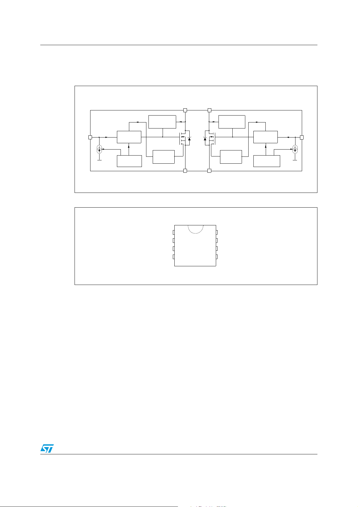
VNS3NV04D-E Block diagram and pin description
1 Block diagram and pin description
Figure 1. Block diagram
DRAIN1
OVERVO LTAGE
CLAMP
INPUT1
GATE
CONTROL
OVER
TEMPERATURE
LINEAR
CURRENT
LIMITER
SOURCE1
Figure 2. Configuration diagram (top view)
SOURCE 1
INPUT 1
SOURCE 2
INPUT 2
1
4
DRAIN2
SOURCE2
8
5
OVERVO LTAGE
CLAMP
LINEAR
CURRENT
LIMITER
DRAIN 1
DRAIN 1
DRAIN 2
DRAIN 2
GATE
CONTROL
OVER
TEMPERATURE
INPUT2
5/21
Electrical specifications VNS3NV04D-E
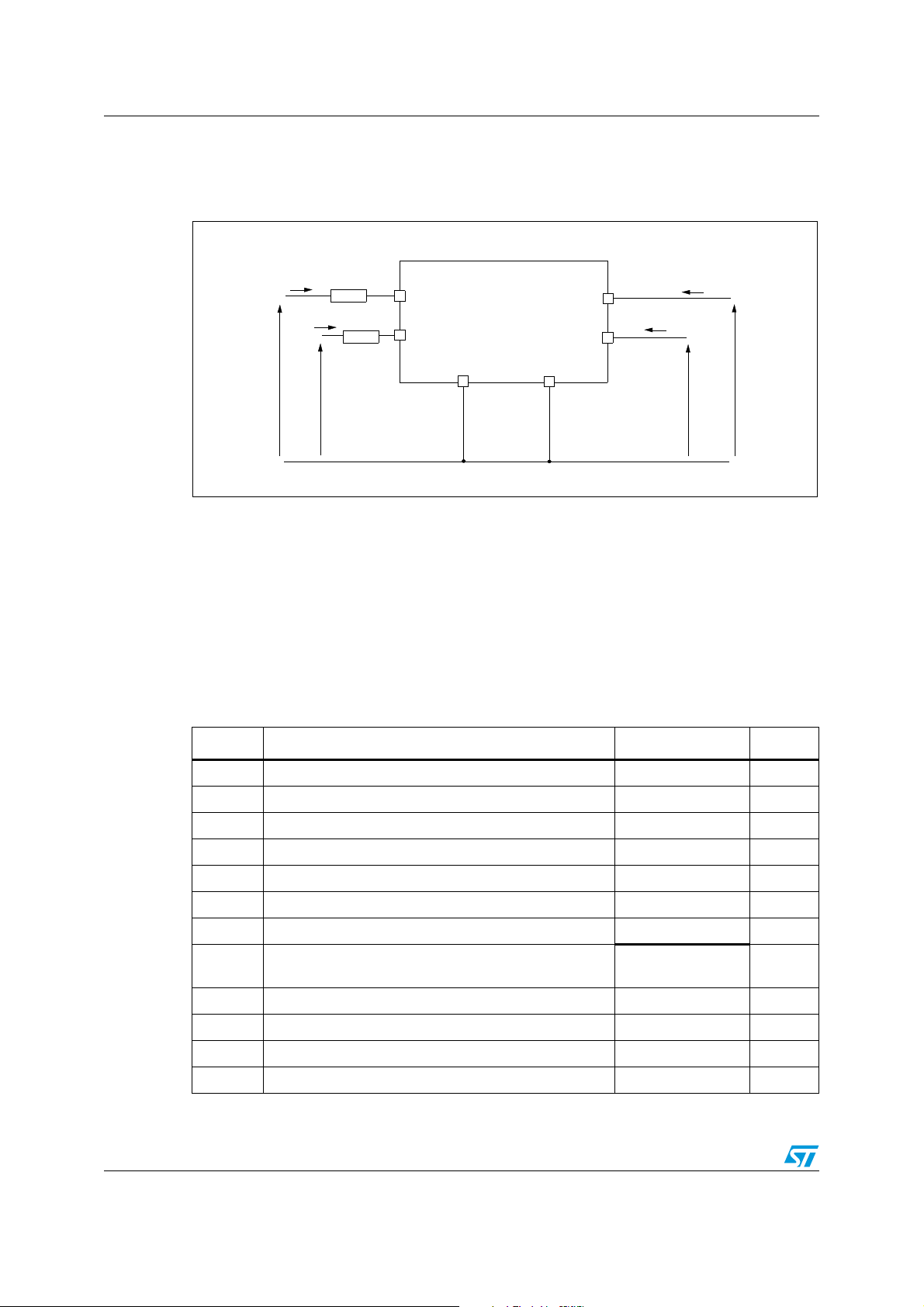
2 Electrical specifications
Figure 3. Current and voltage conventions
IN2
R
IN1
INPUT 1
I
R
IN2
IN2
INPUT 2
SOURCE 1
I
IN1
V
IN1
V
2.1 Absolute maximum ratings
Stressing the device above the rating listed in the “Absolute maximum ratings” table may
cause permanent damage to the device. These are stress ratings only and operation of the
device at these or any other conditions above those indicated in the operating sections of
this specification is not implied. Exposure to Absolute maximum rating conditions for
extended periods may affect device reliability. Refer also to the STMicroelectronics SURE
program and other relevant quality document.
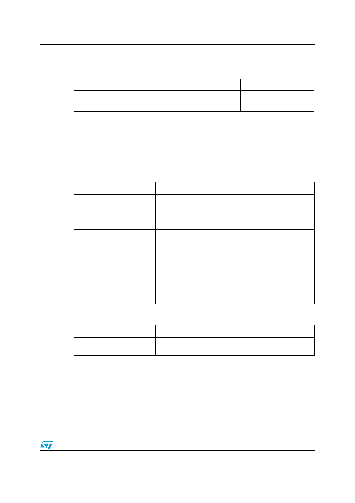
Table 2. Absolute maximum ratings
DRAIN 1
DRAIN 2
SOURCE 2
I
D1
I
D2
V
DS1
V
DS1
Symbol Parameter Value Unit
V
V
I
R
IN MINn
I
I
V
ESD1
V
ESD2
P
T
Drain-Source Voltage (V
DSn
Input voltage Internally clamped V
INn
Input current +/-20 mA
INn
=0V) Internally clamped V
INn
Minimum input series impedance 220 Ω
Drain current Internally limited A
Dn
Reverse DC output current -5.5 A
Rn
Electrostatic discharge (R=1.5KΩ, C=100pF) 4000 V
Electrostatic discharge on output pins only (R=330Ω,
C=150pF)
Total dissipation at Tc=25°C 4 Ω
tot
Operating junction temperature Internally limited °C
T
j
Case operating temperature Internally limited °C
T
c
Storage temperature -55 to 150 °C
stg
6/21
16500 V
VNS3NV04D-E Electrical specifications
2.2 Thermal data
Table 3. Thermal data
Symbol Parameter Max value Unit
R
thj-lead
R
thj-amb
1. When mounted on a standard single-sided FR4 board with 50mm2 of Cu (at least 35 µm thick) connected
to all DRAIN pins of the relative channel
Thermal resistance junction-lead (per channel) 30 °C/W
Thermal resistance junction-ambient 80
2.3 Electrical characteristics
Values specified in this section are for -40°C< Tj <150°C, unless otherwise stated.
Table 4. Off
Symbol Parameter Test Conditions Min Typ Max Unit
V
CLAMP
V
CLTH
V
INTH
I
V
INCL
Drain-Source clamp
voltage
Drain-Source clamp
threshold voltage
Input threshold
voltage
Supply current from
ISS
input pin
Input-Source clamp
voltage
VIN=0V; ID=1.5A 40 45 55 V
=0V; ID=2mA 36 V
V
IN
V
DS=VIN
V
=0V; VIN=5V 100 150 µA
DS
IIN=1mA
IIN=-1mA
(1)
°C/W
; ID=1mA 0.5 2.5 V
6
6.8 8
-1.0
-0.3
V
I
DSS
Zero input voltage
drain current
(VIN=0V)
VDS=13V; VIN=0V; Tj=25°C
VDS=25V; VIN=0V
30
75
Table 5. On
Symbol Parameter Test conditions Min Typ Max Unit
R
DS(on)
Static Drain-Source
On resistance
=5V; ID=1.5A; Tj=25°C
V
IN
=5V; ID=1.5A
V
IN
7/21
120
240
µA
mΩ
 Loading...