

®
VNS3NV04D
“OMNIFE T II” :
FULLY AUTOPROTECTED POWER MOSFET
TYPE R
DS(on)
I
lim
V
clamp
VNS3NV04D 120 mΩ (*) 3.5 A (*) 40 V (*)
(*)Per each device
n
LINEAR CURRENT LIMITATION
n
THERMAL SHUT DOWN
n
SHORT CIRCUIT PROTECTION
n
INTEGRATED CLAMP
n
LOW CURRENT DRAWN FRO M INPUT PIN
n
DIAGNOSTIC FEEDBACK THROUGH INPUT
PIN
n
ESD PROTECTION
n
DIRECT ACCESS TO THE GATE OF THE
POWER MOSFET (ANALOG DRIVING)
n
COMPATIBLE WITH STANDARD POWER
MOSFET
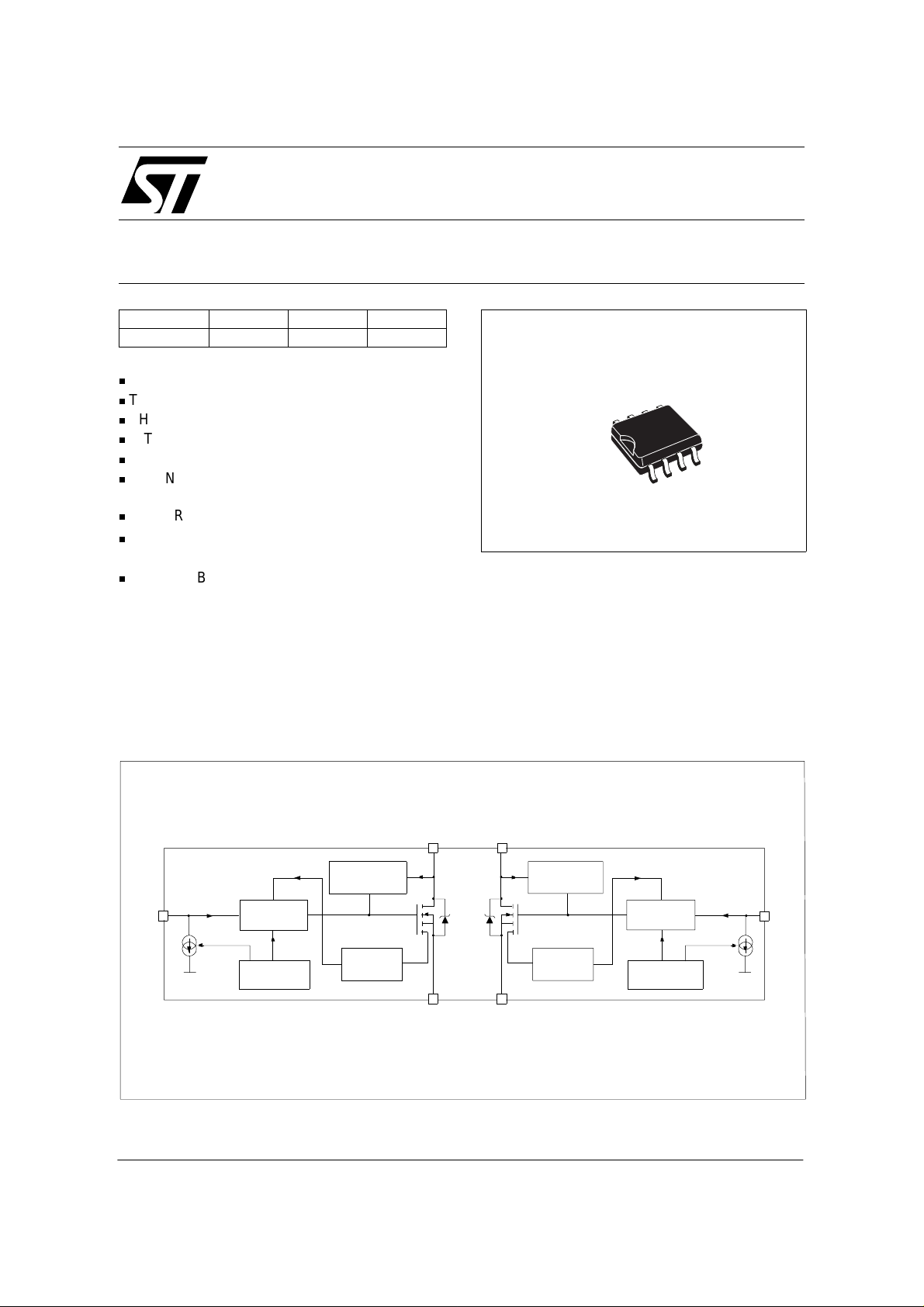
DESCRIPTION
The VNS3NV04D is a device formed by two
monolithic OMNIFET II chips housed in a
standard SO-8 package. The OMNIFET II are
designed in STMicroelectronics VIPower M0-3
Technology: they ar e intended for rep lacement of
standard Po wer M OS FETS fr om DC up t o 50 KHz
BLOCK DIAGRAM
SO-8
applications. Built in thermal shutdown, linear
current limitation and overvoltage clamp protects
the chip in harsh environments.
Fault feedback ca n be dete c ted by mo nitori ng the
voltage at the input pin.
DRAIN2
SOURCE2
OVERVOLTAGE
CLAMP
LINEAR
CURRENT
LIMITER
GATE
CONTROL
OVER
TEMPERATURE
INPUT2
INPUT1
GATE
CONTROL
OVER
TEMPERATURE
OVERVOLTAGE
CLAMP
LINEAR
CURRENT
LIMITER
DRAIN1
SOURCE1
Februa ry 2003 1/14
1
VNS3NV04D
ABSOLUTE MAXIMUM RATI NG
Symbol Parameter Value Unit
V
V
I
R
IN MINn
I
I
V
ESD1
V
ESD2
P
T
DSn
INn
INn
Dn
Rn
T
T
stg
Drain-source Voltage (V
Input Vol tage Internally Clamp ed V
Input Current +/-20 mA
Minimum I nput Series Impedance 220 Ω
Drain Current Internally Limited A
Reverse DC Output Current -5.5 A
Electros tatic Discharge (R=1.5KΩ, C=100pF) 4000 V
Electros tatic Discharge on output pins only (R=330Ω, C=150pF) 16500 V
Total Dissipation at Tc=25°C 4 W
tot
Operating Junction Temperature Internally limited °C
j
Case Operating Temperature Internally limited °C
c
Storage Temperature -55 to 150 °C
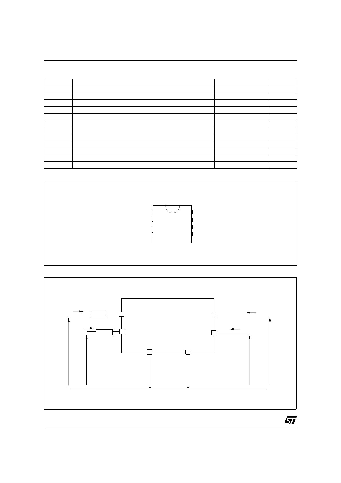
CONNECTION DIAGRAM (TO P VI EW)
=0V) Intern ally Clamped V
INn
SOURCE 1
INPUT 1
SOURCE 2
INPUT 2
CURRENT AND VOLTAGE CONV ENTIONS
I
IN1
V
IN1
V
IN2
R
IN1
INPUT 1
I
IN2
R
IN2
INPUT 2
SOURCE 1
1
4
8
5
DRAIN 1
DRAIN 2
SOURCE 2
DRAIN 1
DRAIN 1
DRAIN 2
DRAIN 2
I
D1
I
D2
V
DS1
V
DS1
2/14
1

VNS3NV04D
THERMAL DATA
Symbol Parameter Value Unit
R
thj-lead
R
thj-amb
(*) When mounted on a standard s ingle-sided FR4 boar d with 50mm
channel.
ELECTRICAL CHARACTERISTICS (-40°C < Tj < 150°C, unless otherwise specified)
(Per each device)
OFF
Symbol Parameter Test Conditions Min Typ Max Unit
V
CLAMP
V
CLTH
V
INTH
I
ISS
V
INCL
I
DSS
Ther m al Re s i st an ce Junction-lead (per channe l ) MAX 30 °C/W
Thermal Resistance Junction-ambient MAX 80(*) °C/W
2
of Cu (at least 35 µm thick) connected to all DRAIN pins of the relative
Drain-source Clamp
Voltage
Drain-source Clamp
Threshold Voltage
V
=0V; ID=1.5A 40 45 55 V
IN
VIN=0V; ID=2mA 36 V
Input Thre shold Voltage VDS=VIN; ID=1mA 0.5 2.5 V
Supply Current from Input
Pin
Input-Source Clamp
Voltage
Zero Input Voltage Drain
Current (VIN=0V)
VDS=0V; VIN=5V 100 150 µA
IIN=1mA
I
=-1mA
IN
=13V; VIN=0V; Tj=25°C
V
DS
V
=25V; VIN=0V
DS
6
-1.0
6.8 8
-0.3
30
75
V
µA
ON
Symbol Parameter Test Conditions Min Typ Max Unit
R
DS(on)
Static Drain-source On
Resistance
=5V; ID=1.5A; Tj=25°C
V
IN
V
=5V; ID=1.5A
IN
120
240
mΩ
3/14
1

VNS3NV04D
ELECTRICAL CHARACTERISTICS (continued) (Tj=25°C, unless otherwise specified)
DYNAMIC
Symbol Parameter Test Condit ions Min Typ Max Unit
gfs (*)
C
OSS
SWITCHING
Symbol Parameter Test Conditi ons Min Typ Max Unit
t
d(on)
t
t
d(off)
t
t
d(on)
t
t
d(off)
t
(dI/dt)
Q
Forward
Transconductanc e
VDD=13V; ID=1.5A 5.0 S
Output Capacitance VDS=13V; f=1MHz; VIN=0V 150 pF
Turn-on Delay Time
Rise Time 250 750 ns
r
Turn-off Delay Time 450 1350 ns
Fall Time 250 750 ns
f
Turn-on Delay Time
Rise Time 2.5 7.5 µs
r
Turn-off Delay Time 3.3 10.0 µs
Fall Time 2.0 6.0 µs
f
Turn-on Current Slope
on
Total Input Charge
i
=15V; ID=1.5A
V
DD
V
=5V; R
gen
gen=RIN MINn
(see figure 1)
=15V; ID=1.5A
V
DD
V
gen
=5V; R
gen
=2.2K Ω
(see figure 1)
=15V; ID=1.5A
V
DD
V
=5V; R
V
I
gen
DD
gen
gen=RIN MINn
=12V; ID=1.5A; VIN=5V
=2.13mA (see figure 5)
=220Ω
=220Ω
90 300 ns
0.45 1.35 µs
4.7 A/µs
8.5 nC
SOURCE DRAIN DIODE
Symbol Parameter Test Conditions Min Typ Max Unit
(*) Forward On Voltage ISD=1.5A; VIN=0V 0.8 V
V
SD
Q
I
RRM
t
Reverse Recovery Time ISD=1.5A; dI/dt=12A/µs
rr
Reverse Recovery Charge 37 µC
rr
Reverse Recovery Current 0.7 A
V
=30V; L= 20 0 µ H
DD
(see test circuit, figure 2)
107 ns
PROTECTIONS (-40°C < Tj < 150°C, unless otherwise specified)
Symbol Parameter Test Conditions Min Typ Max Unit
I
lim
t
dlim
T
T
I
E
(*) Pulsed: Pu ls e duration = 300µs, duty c y c le 1.5%
Drain Current Limit VIN=5V; VDS=13V 3.5 5 7 A
=5V; VDS=13V
Step Response Current
Limit
Overtemperature
jsh
Shutdown
Overtemperature Reset 135 °C
jrs
Fault Sink Current VIN=5V; VDS=13V; Tj=T
gf
Sing l e Pu lse
as
Avala nche Energy
V
IN
starti ng T
V
IN
=25°C; VDD=24V
j
=5V; R
gen=RIN MINn
(see figures 3 & 4)
jsh
=220Ω; L=24mH
10 µs
150 175 200 °C
10 15 20 mA
100 mJ
4/14
2

VNS3NV04D
PROTECTION FEATURES
During normal operation, the INPUT pin is
electrically connected to the gate of the internal
power MOSFET through a low impedance path.
The device then behaves like a standard power
MOSFET and can be used as a switch from DC to
50KHz. The only difference from the user’s
standpoint is that a small DC current I
100µA) flows into the INPUT pin in order to supply
ISS
(typ.
the internal circuitry.
The de vice integrates :
- OVERVOLTAGE CLAMP PROTECTION:
internally set at 45V, along with the rugged
avalanche characteristics o f the Power MOSFET
stage giv e this device unrivall ed ruggedne ss and
energy handl ing capability. This feat ure is mainly
important when driving inductive loads.
- LINEAR CURRENT LIMITER CIRCUIT: limits
the drain current ID to I
voltage. When the current limiter is active, the
whatever the INPUT pin
lim
device operates in the linear region, so power
dissipation may exceed the capability of the
heatsink. Both case and junction temperatures
increase, and if this phase lasts long enough,
junction temperature may reach the
overtemperature threshold T
jsh
.
- OVERTEMPERATURE AND SHORT CIRCUIT
PROTECTION: these are based on sensing the
chip temperature and are not dependent on the
input voltage. The location of the sensi ng eleme nt
on the chip in the power st age ar ea ensures f ast,
accurate detection of the junction temperature.
Overtemperature cutout occurs in the range 150 to
190 °C, a typical value being 170 °C. The device is
automatically restarted when the chip temperature
falls of about 15°C below shut-down temperature.
- STATUS FEEDBACK: in the case of an
overtemperature fault condition (Tj > T
device tries to sink a diagnostic current Igf thro ug h
jsh
), the
the INPUT pin in order to indicate fault condition. If
driven from a l ow impedance sou rce, this curre nt
may be used in orde r to warn the contr ol circ uit of
a device shut down. If the drive impeda nc e is h i gh
enough so that the INPUT pin dri ver is not abl e to
supply the current Igf, the INPUT pin will fall to 0V.
This will not however affect the device
operation: no requirement is put on the current
capability of t he IN PUT pin dr ive r e xcep t t o b e
able to supply the normal operation drive
current I
ISS
.
Additional features of this device are ESD
protection according to the Human Body model
and the ability to be driven from a TTL Logic
circuit.
5/14
1
 Loading...