

VNQ690SP-E
QUAD CHANNEL HIGH SIDE DRIVER
Table 1. General Features
Type R
VNQ690SP-E 90m
DS(on)
Ω (*) 10A 36V
(*) Per each channel
OUTPUT CURRENT PER CHANNEL: 10A
■
■ CMOS COMPATIBLE INPUTS
■ OPEN LOAD DETECTION (OFF STATE)
■ UNDERVOLTAGE & OVERVOLTAGE
n
SHUT- DOWN
■ OVERVOLTAGE CLAMP
■ THER MAL SH U T-DOWN
■ CURRENT LIMITATION
■ VERY LOW STAND-BY POWER DISSIPATION
■ PROTEC TI ON AG A INS T:
n
LOSS OF GROUND & LOSS OF V
■ REVERSE BATTERY PROTECTION (**)
■ IN COMPLIANCE WITH THE 2002/95/EC
I
out
CC
V
CC
EUROPEAN DIRECTIVE
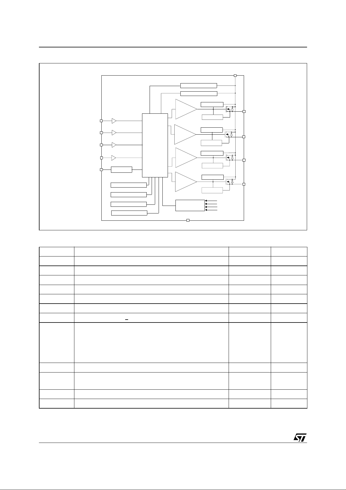
DESCRIPTION
The VNQ690SP-E is a monolithic device made by
using| STMicroelectronics VIPower M0-3
Technology, intended for driving resistive or
inductive loads with one side connected to ground.
This device has four independent channels.
Built-in thermal shut down and output current
limitation protect the chip from over temperature
and short circuit.
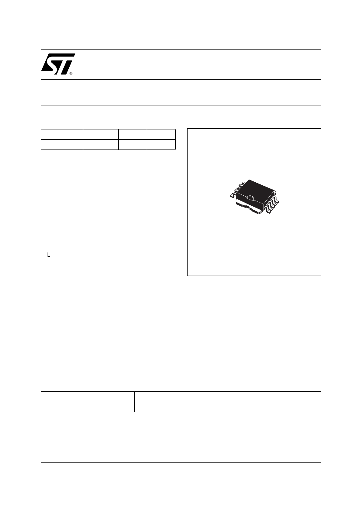
Figure 1. Package
10
1
PowerSO-10™
Table 2. Order Codes
Package Tube Tape and Reel
PowerSO-10™
Note: (**) See application schematic at page 9
VNQ690SP-E VNQ690SPTR-E
Rev. 1
1/20October 2004
VNQ690SP-E
Figure 2. Block Diagram
OVERVOLT AGE
UNDERVOLT AGE
V
CC
DEMAG 1
I
LIM1
DEMAG 2
I
LIM2
DEMAG 3
I
LIM3
DEMAG 4
I
LIM4
OUTPUT 1
OUTPUT 2
OUTPUT 3
OUTPUT 4
INPUT 1
INPUT 2
INPUT 3
INPUT 4
STATUS
STATUS
OVERTEMP. 1
OVERTEMP. 2
OVERTEMP. 3
OVERTEMP. 4
LOGIC
DRIVER 1
DRIVER 2
DRIVER 3
DRIVER 4
OPEN LOAD
OFF-STATE
GND
Table 3. Absolute Maximum Ratings
Symbol Parameter Value Unit
V
-V
I
OUT
I
I
I
STAT
I
GND
V
ESD
P
E
MAX
T
T
CC
CC
R
IN
tot
j
stg
Supply voltage (continuous) 41 V
Reverse supply voltage (continuous) -0.3 V
Output current (continuous), per each channel Internally limited A
Reverse output current (continuous), per each channel -15 A
Input current +/- 10 mA
Status current +/- 10 mA
Ground current at TC<25°C (continuous) -200 mA
Electrostatic Discharge (Human Body Model: R=1.5KΩ; C=100pF)
- INPUT
- STATUS
- OUTPUT
- V
CC
4000
4000
5000
5000
Power dissipation at TC=25°C78W
Maximum Switching Energy
(L=0.38mH; R
=0Ω; V
L
=13.5V; T
bat
=150ºC; IL=14A)
jstart
53 mJ
Junction operating temperature -40 to 150 °C
Storage temperature -65 to 150 °C
V
V
V
V
2/20
VNQ690SP-E
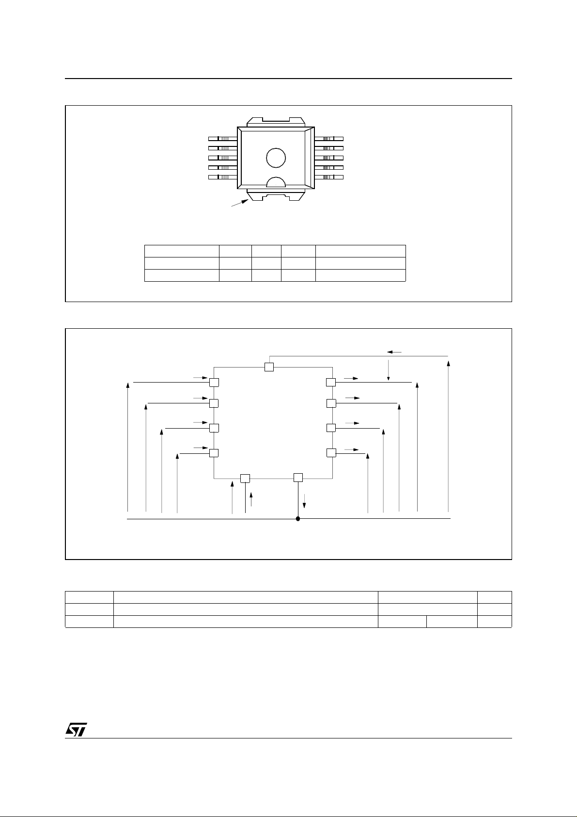
Figure 3. Con fig urat i on Dia g ra m (Top View) & Sugg est ed C o nnections for Unused and N.C. Pins
STATUS
INPUT 4
INPUT 3
INP UT 2
INPUT 1
6
7
8
9
10
11
V
CC
Connection / Pin Status N.C. Output Input
Floating X X X X
To Ground X Through 10KΩ resistor
Figure 4. Current and Voltage Conventions
I
IN1
I
V
IN1
V
IN2
IN2
I
IN3
I
V
IN4
IN3
V
IN4
INPUT 1
INPUT 2
INPUT 3
INPUT 4
STATUS
V
CC
5
4
3
2
1
OUTPUT 1
OUTPUT 2
OUTPUT 3
OUTPUT 4
GND
GND
OUTPUT 4
OUTPUT 3
OUTPUT 2
OUTPUT 1
I
OUT1
I
OUT2
I
OUT3
I
OUT4
V
OUT4
V
V
F1
V
OUT3
(*)
OUT2
V
I
S
OUT1
V
CC
(*) VFn = V
CCn
- V
V
STAT
during reverse battery condition
OUTn
I
STAT
I
GND
Table 4. Thermal Data
Symbol Parameter Value Unit
R
thj-case
R
tj-amb
Note: 1.
Note: 2.
Thermal resistance junction-case (MAX) per channel 2 °C/W
Thermal resistance junction-ambient (MAX) 52
When mount ed on a standar d si ngle-sid ed F R-4 board with 0.5cm² of Cu (at least 35 µm thick)
When mounted on a stan dard single-sided FR-4 board with 6cm² of Cu (at le ast 35 µm thick).
(1)
37
(2)
°C/W
3/20
VNQ690SP-E
ELECTRICAL CHARACTERISTICS
=6V up to 24V; -40°C<Tj<150°C unless otherwise specified)
(V
CC
Table 5. Power (Per each channel)
Symbol Parameter Test Conditions Min. Typ. Max. Unit
(#) Operating supply voltage 6 13 36 V
V
CC
(#) Undervoltage shutdown 3.5 4.6 6 V
V
USD
(#) Undervoltage hysteresis 0.2 1 V
V
UVhyst
V
(#) Overvoltage shutdown 36 V
OV
V
(#) Overvoltage hysteresis 0.25 V
OVhyst
(#) Supply current
I
S
Off state; V
Off state; V
=25°C
T
j
On state; V
IN=VOUT
IN=VOUT
IN
=0V; VCC=13.5V
=0V; VCC=13.5V
=3.25V; 9V<VCC<18V
12
12
6
40
25
12
µA
µA
mA
R
ON
I
L(off1)
I
L(off2)
I
L(off3)
I
L(off4)
Note: (#) Per device.
On state resistance
Off State Output Current VIN=V
Off State Output Current VIN=0V; V
Off State Output Current VIN=V
Off State Output Current VIN=V
I
=1A; Tj=25°C; 9V<VCC<18V
OUT
=1A, Tj=150°C; 9V<VCC<18V
I
OUT
=0V 0 50 µA
OUT
=3.5V -75 0 µA
OUT
=0V; VCC=13V; Tj =125°C 5 µA
OUT
=0V; VCC=13V; Tj =25°C 3 µA
OUT
90
180mΩmΩ
Table 6. Protection (see note 1)
(per each channel)
Symbol Parameter Test Conditions Min. Typ. Max. Unit
T
TSD
T
T
hyst
I
LIM
V
demag
V
STAT
I
LSTAT
C
STAT
V
SCL
Note: 1. To ensure long term reliability under heavy overload or short circuit conditions, protection and related diagnostic signals must be
Shutdown temperatur e 150 170 2 00 °C
Reset temperature 135 °C
R
Thermal hysteresis 7 15 25 °C
DC Short circuit current
Turn-off output voltage
clamp
Status low output
voltage
9V<V
6V<V
I
I
Status leakage current Normal operation; V
Status pin input
capacitance
Status clamp voltage
used together with a proper software strategy. If the device is subjected to abnormal conditions, this software must limit the duration
and number of activation cycles
Normal operation; V
I
I
<36V
CC
<36V
CC
=2A; VIN=0V; L=6mH VCC-41 VCC-48 VCC-55 V
OUT
=1.6mA 0.5 V
STAT
=5V 10 µA
STAT
=5V 25 pF
STAT
=1mA
STAT
=-1mA
STAT
10 14 20
20
66.8
-0.7
8V
A
A
V
4/20
ELECTRICAL CHARACTERISTICS (continued)
VNQ690SP-E
Table 7. V
- Output Diode
CC
Symbol Parameter Test Conditions Min Typ Max Unit
V
Table 8. Switching (V
Forward on Voltage -I
F
CC
=13V)
=0.9A; Tj=150°C 0.6 V
OUT
Symbol Parameter Test Conditions Min Typ Max Unit
t
d(on)
t
d(off)
Turn-on delay time RL=13Ω channels 1,2,3,4 30 µs
Turn-off delay time RL=13Ω channels 1,2,3,4 30 µs
See
dV
/dt
OUT
Turn-on voltage slope RL=13Ω channels 1,2,3,4
(on)
relative
diagram
See
dV
/dt
OUT
Turn-off voltage slope RL=13Ω channels 1,2,3,4
(off)
relative
diagram
Table 9. Openload Detection
(off state) per each channel
Symbol Parameter Test Conditions Min Typ Max Unit
t
V
T
SDL
OL
DOL
Status Delay
Openload Voltage
Detection Threshold
Openload Detection Delay
at Turn Off
See Figure 1 (Openload detection
reading must be performed after T
V
=0V 1.5 2.5 3.5 V
IN
DOL
).
20 µs
VCC=18V 300 µs
V/µs
V/µs
Table 10. Logic Input
Symbol Parameter Test Conditions Min Typ Max Unit
V
V
V
V
HYST
I
I
Input Low Level Voltage 1.25 V
IL
Input High Level Voltage 3.25 V
IH
Input Hysteresis Voltage 0.5 V
Input high level voltage VIN=3.25V 10 µA
IH
Input Current VIN=1.25V 1 µA
IL
Input Clamp Voltage IIN=1mA
ICL
I
IN
=-1mA
6 6.8
-0.7
8V
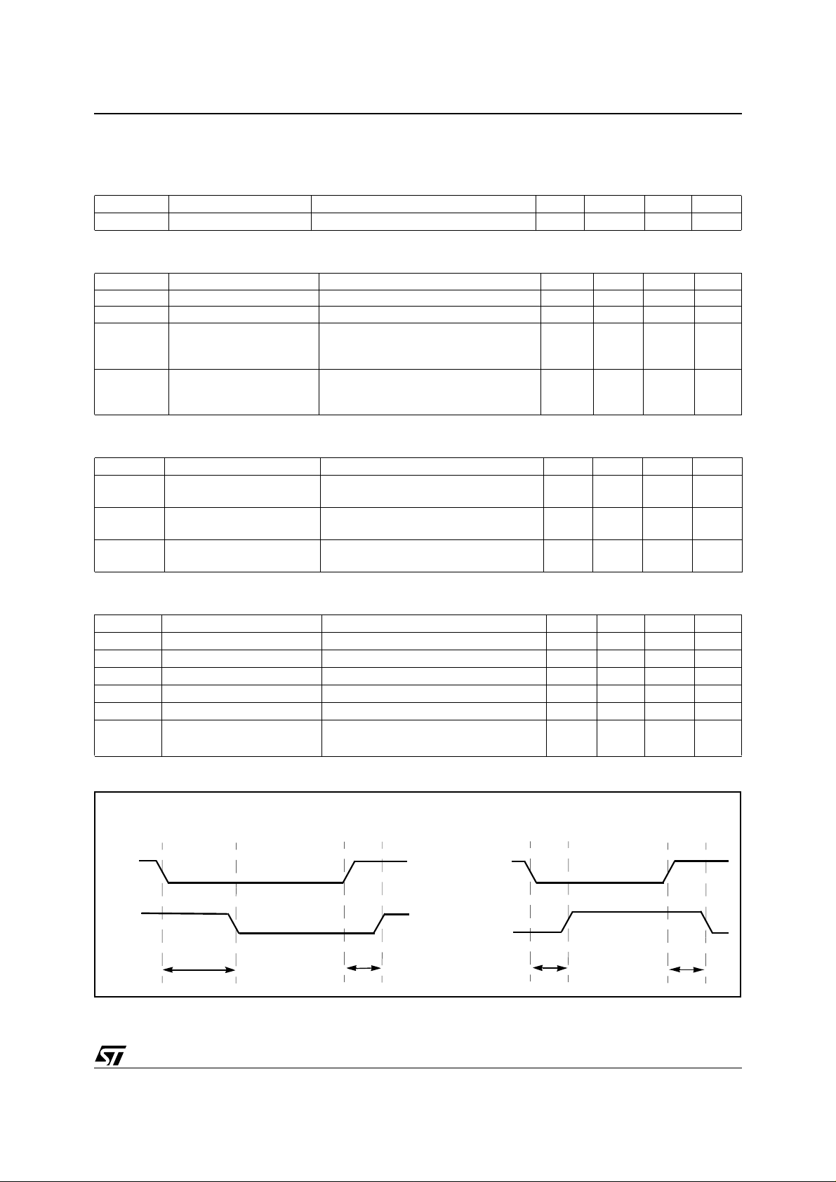
Figure 5. Statu s Ti m in g Wa veforms
V
V
IN
STAT
OPENLOAD STATUS TIMING
t
DOL
t
VIN
V
SDL
OVERTEMP STATUS TIMING
STAT
t
SDL
t
SDL
V
5/20
VNQ690SP-E
Tabl e 11. Truth Table (Per each channel)
CONDITIONS INPUT OUTPUT SENSE
Normal Operation
Overtemperature
Undervoltage
Overvoltage
Current Limitation
Output Voltage > V
OL
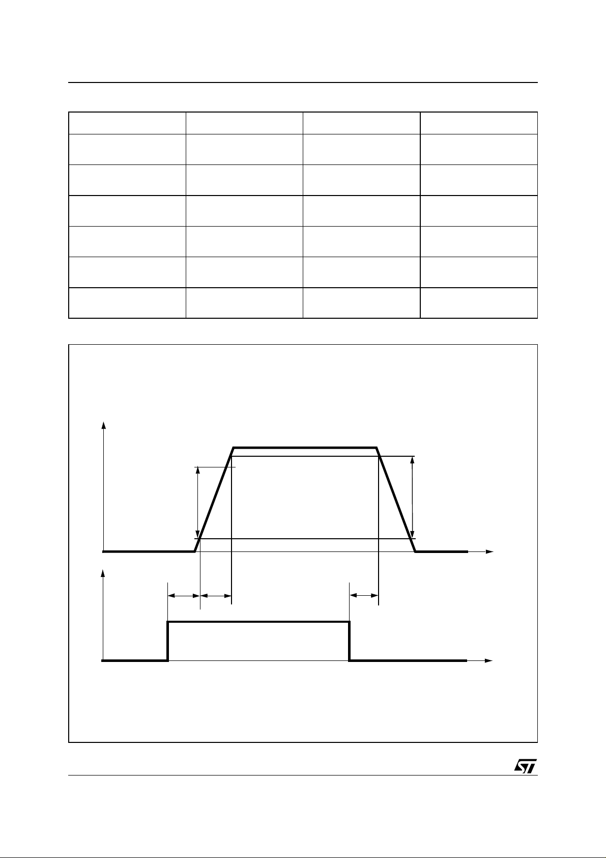
Figure 6. Switching Characteristics
V
LOAD
L
H
L
H
L
H
L
H
L
H
L
H
L
H
L
L
L
L
L
L
L
X
H
H
H
H
H
L
X
X
H
H
H
H
L
H
90%
80%
dV
/dt
OUT
dV
OUT
/dt
(on)
(off)
10%
t
V
IN
t
d(on)
t
r
t
d(off)
t
6/20
 Loading...