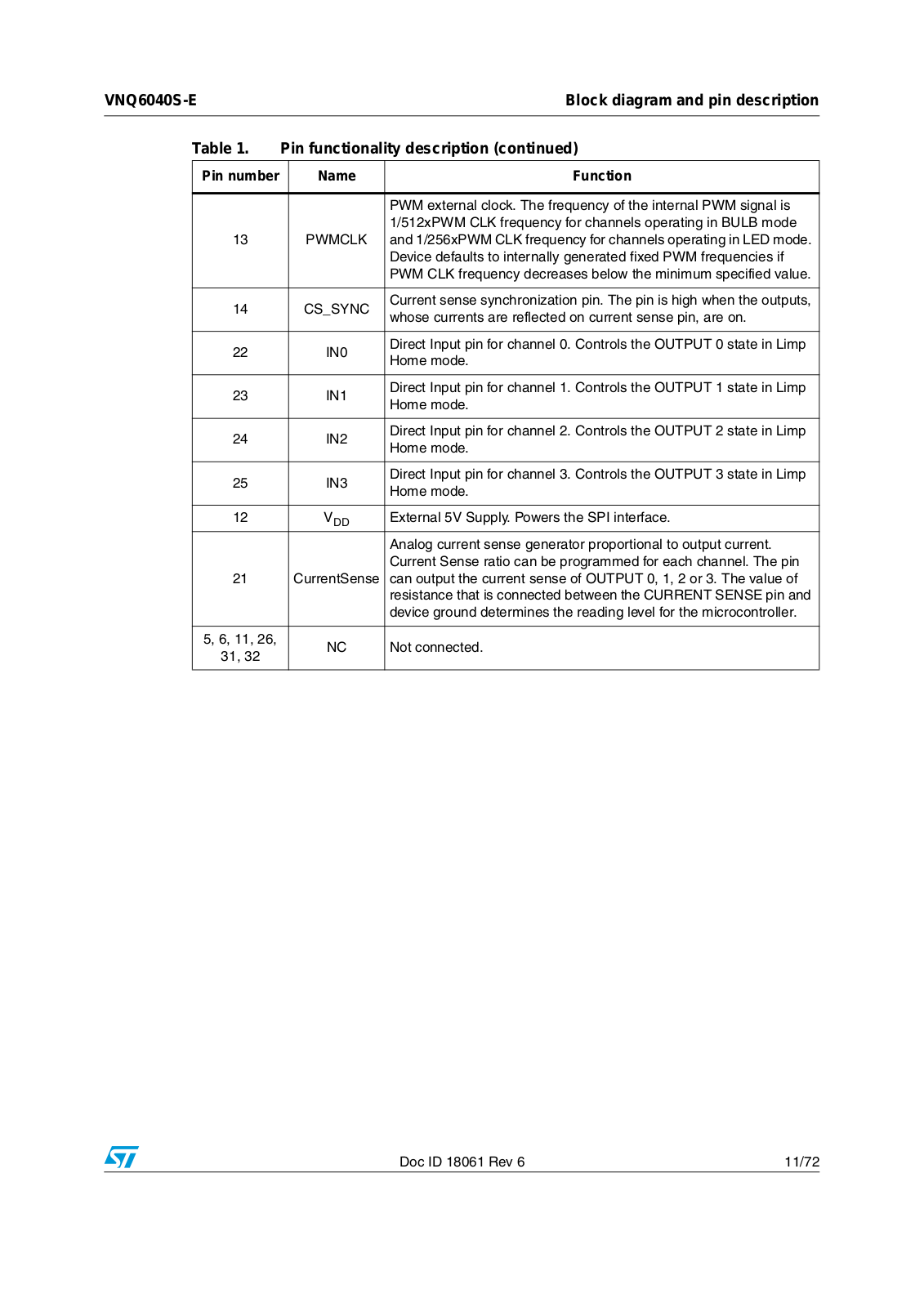
ST VNQ6040S-E User Manual

VNQ6040S-E

Quad channel high-side driver

Features

Channel

VCC

RON (typ)

ILIMH (min)

Channel0-3

41 V

35 mΩ

25 A


General

16 bit ST-SPI for full and diagnostic

Programmable BULB/LED mode

Integrated PWM and phase shift generation unit

120 Hz internal PWM fallback frequency

Advanced limp home functionalities for robust fail-safe system

Very low standby current

Optimized electromagnetic emissions

Very low electromagnetic susceptibility

In compliance with the 2002/95/EC

Diagnostic

Multiplex proportional load current sense

Synchronous diagnostic of overload and

short to GND, output shorted to VCC, ON-state and OFF-state open-load

Programmable case overtemperature warning

Protections

Load current limitation

Self limiting of fast thermal transients

Power limitation and overtemperature shutdown (latching off or autorestart)

Undervoltage shutdown

Overvoltage clamp

Reverse battery protected through power outputs self turn-on (no external components)

Load dump protected

Protection against loss of ground

Datasheet production data

PowerSSO-36

Description

The VNQ6040S-E is a device made using STMicroelectronics® VIPower® technology. It is intended for driving resistive or inductive loads directly connected to ground. The device is protected against voltage transient on VCC pin.

Programming, control and diagnostics are implemented via the SPI bus.

An analog current feedback for each channel is connected to the CURRENT-SENSE pin via a multiplexer. A CS_SYNC pin delivers a synchronous signal for sampling the current sense while the corresponding output is on.

The device detects open-load for both on-state and off-state conditions.

Real time diagnostic is available through the SPI bus (open-load, output short to VCC, overtemperature, communication error).

Output current limitation protects the device in an overload condition. The device can limit the dissipated power to a safe level up to thermal shutdown intervention. Thermal shutdown can be configured as latched off or with automatic restart.

The device enters a limp home mode in case of loss of digital supply (VDD), reset of digital memory or CSN monitoring time-out event. In this mode states of channel 0, 1, 2 or 3 are respectively controlled by four dedicated pins IN0, IN1, IN2 and IN3. Each channel can be programmed in BULB/LED mode.

July 2012

Doc ID 18061 Rev 6

1/72

This is information on a product in full production.

www.st.com

Contents

VNQ6040S-E


Contents

1

Block diagram and pin description . . . . . . . . . . . . . . . . . . . . . . . . . . . .

. 8

2

Functional description . . . . . . . . . . . . . . . . . . . . . . . . . . . . . . . . . . . . . .

12


2.1

Operating modes . . . . . . . . . . . . . . . . . . . . . . . . . . . . . . . . . . . . . . . . . . .

12

2.1.1 Reset mode . . . . . . . . . . . . . . . . . . . . . . . . . . . . . . . . . . . . . . . . . . . . . . 14 2.1.2 Fail Safe mode . . . . . . . . . . . . . . . . . . . . . . . . . . . . . . . . . . . . . . . . . . . . 14 2.1.3 Normal mode . . . . . . . . . . . . . . . . . . . . . . . . . . . . . . . . . . . . . . . . . . . . . 15 2.1.4 Standby mode . . . . . . . . . . . . . . . . . . . . . . . . . . . . . . . . . . . . . . . . . . . . 16 2.1.5 Sleep mode 1 . . . . . . . . . . . . . . . . . . . . . . . . . . . . . . . . . . . . . . . . . . . . . 16 2.1.6 Sleep mode 2 . . . . . . . . . . . . . . . . . . . . . . . . . . . . . . . . . . . . . . . . . . . . . 16 2.1.7 Battery undervoltage mode . . . . . . . . . . . . . . . . . . . . . . . . . . . . . . . . . . 16

2.2

Programmable functions . . . . . . . . . . . . . . . . . . . . . . . . . . . . . . . . . . . . .

19


2.2.1

Outputs configuration . . . . . . . . . . . . . . . . . . . . . . . . . . . . . . . . . . . . . . .

19


2.2.2

Case over temperature . . . . . . . . . . . . . . . . . . . . . . . . . . . . . . . . . . . . .

20


2.2.3

Protections . . . . . . . . . . . . . . . . . . . . . . . . . . . . . . . . . . . . . . . . . . . . . . .

21


2.2.4

Open-load ON-state detection . . . . . . . . . . . . . . . . . . . . . . . . . . . . . . . .

22


2.2.5

Open-load OFF-state detection . . . . . . . . . . . . . . . . . . . . . . . . . . . . . . .

23


2.2.6

Current sense . . . . . . . . . . . . . . . . . . . . . . . . . . . . . . . . . . . . . . . . . . . .

24

2.3 Test mode (reserved) . . . . . . . . . . . . . . . . . . . . . . . . . . . . . . . . . . . . . . . . 25

3

SPI functional description . . . . . . . . . . . . . . . . . . . . . . . . . . . . . . . . . . .

26


3.1

SPI communication . . . . . . . . . . . . . . . . . . . . . . . . . . . . . . . . . . . . . . . . .

26

3.1.1 Signal description . . . . . . . . . . . . . . . . . . . . . . . . . . . . . . . . . . . . . . . . . 26 3.1.2 Connecting to the SPI bus . . . . . . . . . . . . . . . . . . . . . . . . . . . . . . . . . . . 26 3.1.3 SPI mode . . . . . . . . . . . . . . . . . . . . . . . . . . . . . . . . . . . . . . . . . . . . . . . . 26

3.2 SPI protocol . . . . . . . . . . . . . . . . . . . . . . . . . . . . . . . . . . . . . . . . . . . . . . . 27

3.2.1 SDI, SDO format . . . . . . . . . . . . . . . . . . . . . . . . . . . . . . . . . . . . . . . . . . 27 3.2.2 Global status byte description . . . . . . . . . . . . . . . . . . . . . . . . . . . . . . . . 28 3.2.3 Operating code definition . . . . . . . . . . . . . . . . . . . . . . . . . . . . . . . . . . . . 29

3.3 Address mapping . . . . . . . . . . . . . . . . . . . . . . . . . . . . . . . . . . . . . . . . . . . 32

3.3.1 Address 00h - Control Register (CTLR) . . . . . . . . . . . . . . . . . . . . . . . . . 33 3.3.2 Address 01h - SPI Output Control Register (SOCR) . . . . . . . . . . . . . . . 34 3.3.3 Address 02h - Direct Input Enable Control Register (DIENCR) . . . . . . . 35

2/72

Doc ID 18061 Rev 6

VNQ6040S-E

Contents


3.3.4Address 03h - Current Sense Multiplexer Control Register (CSMUXCR) .

. . . . . . . . . . . . . . . . . . . . . . . . . . . . . . . . . . . . . . . . . . . . . . . . . . . . . . . . 35

3.3.5Address 04h - Current Sense Ratio Control Register (CSRATCR) . . . . 36

3.3.6 Address 05h - PWM Mode Control Register (PWMCR) . . . . . . . . . . . . 36 3.3.7 Address 06h - Open-load ON-State Control Register (OLONCR) . . . . . 36 3.3.8 Address 07h - Open-load OFF-State Control Register (OLOFFCR) . . . 37

3.3.9Address 08h - Automatic Shutdown Control Register (ASDTCR) . . . . . 37

3.3.10 Address 09h - Channel Control Register (CCR) . . . . . . . . . . . . . . . . . . 37 3.3.11 Address 10h - 13h - Duty Cycle Control Register (DUTYXCR) . . . . . . . 38 3.3.12 Address 18h - 1Ah - Phase Control Register (PHASEXCR) . . . . . . . . . 38 3.3.13 Address 2Eh - Channel Read Back Status Register (CHDRVR) . . . . . . 39 3.3.14 Address 2Fh - General Status Register (GENSTR) . . . . . . . . . . . . . . . 39 3.3.15 Address 30h - Over Temperature Status Register (OTFLTR) . . . . . . . . 40 3.3.16 Address 31h - Open-Load ON-State Status Register (OLFLTR) . . . . . . 41

3.3.17Address 32h - Open-Load OFF-State / Stuck to VCC Status Register

(STKFLTR) . . . . . . . . . . . . . . . . . . . . . . . . . . . . . . . . . . . . . . . . . . . . . . . 41 3.3.18 Address 33h - Power Limitation Status Register (PWLMFLTR) . . . . . . . 42 3.3.19 Address 34h - Over Load Status Register (OVLFLTR) . . . . . . . . . . . . . 43 3.3.20 Minimum duty cycle vs frequency . . . . . . . . . . . . . . . . . . . . . . . . . . . . . 43 3.3.21 Address 3Eh - Test Register (TEST) . . . . . . . . . . . . . . . . . . . . . . . . . . . 44 3.3.22 Address 3Fh - Configuration Register (GLOBCTR) . . . . . . . . . . . . . . . . 44

4

Electrical specifications . . . . . . . . . . . . . . . . . . . . . . . . . . . . . . . . . . . . .

46


4.1

Absolute maximum ratings . . . . . . . . . . . . . . . . . . . . . . . . . . . . . . . . . . . .

46


4.2

Thermal data . . . . . . . . . . . . . . . . . . . . . . . . . . . . . . . . . . . . . . . . . . . . . .

47


4.3

Electrical characteristics . . . . . . . . . . . . . . . . . . . . . . . . . . . . . . . . . . . . . .

48

4.3.1 SPI . . . . . . . . . . . . . . . . . . . . . . . . . . . . . . . . . . . . . . . . . . . . . . . . . . . . . 48 4.3.2 BULB mode . . . . . . . . . . . . . . . . . . . . . . . . . . . . . . . . . . . . . . . . . . . . . . 51 4.3.3 LED mode . . . . . . . . . . . . . . . . . . . . . . . . . . . . . . . . . . . . . . . . . . . . . . . 53

4.4 Maximum demagnetization energy (VCC = 13.5 V) . . . . . . . . . . . . . . . . . 61

5

Package and PCB thermal data . . . . . . . . . . . . . . . . . . . . . . . . . . . . . . .

62


5.1

PowerSSO-36 thermal data . . . . . . . . . . . . . . . . . . . . . . . . . . . . . . . . . . .

62

6

Package information . . . . . . . . . . . . . . . . . . . . . . . . . . . . . . . . . . . . . . . .

65


6.1

ECOPACK® package . . . . . . . . . . . . . . . . . . . . . . . . . . . . . . . . . . . . . . . .

65


6.2

PowerSSO-36 mechanical data . . . . . . . . . . . . . . . . . . . . . . . . . . . . . . . .

66

Doc ID 18061 Rev 6

3/72

Contents


VNQ6040S-E


6.3

Packing information . . . . . . . . . . . . . . . . . . . . . . . . . . . . . . . . . .

. . . . . . . 68

7

Order codes . . . . . . . . . . . . . . . . . . . . . . . . . . . . . . . . . . . . . . . . .

. . . . . . 69

8

Revision history . . . . . . . . . . . . . . . . . . . . . . . . . . . . . . . . . . . . .

. . . . . . 70

4/72

Doc ID 18061 Rev 6

VNQ6040S-E

List of tables


List of tables

Table 1. Pin functionality description . . . . . . . . . . . . . . . . . . . . . . . . . . . . . . . . . . . . . . . . . . . . . . . . 10 Table 2. Operating modes . . . . . . . . . . . . . . . . . . . . . . . . . . . . . . . . . . . . . . . . . . . . . . . . . . . . . . . . 13 Table 3. Output control truth table . . . . . . . . . . . . . . . . . . . . . . . . . . . . . . . . . . . . . . . . . . . . . . . . . . 19 Table 4. Example of DUTYCXCR register . . . . . . . . . . . . . . . . . . . . . . . . . . . . . . . . . . . . . . . . . . . . 20 Table 5. Example of PHASEXCR register . . . . . . . . . . . . . . . . . . . . . . . . . . . . . . . . . . . . . . . . . . . . 20 Table 6. Activation of blanking filter in case of power limitation . . . . . . . . . . . . . . . . . . . . . . . . . . . . 22 Table 7. Nominal open-load thresholds . . . . . . . . . . . . . . . . . . . . . . . . . . . . . . . . . . . . . . . . . . . . . . 23 Table 8. STKFLTR state . . . . . . . . . . . . . . . . . . . . . . . . . . . . . . . . . . . . . . . . . . . . . . . . . . . . . . . . . . 24 Table 9. Current sense ratio . . . . . . . . . . . . . . . . . . . . . . . . . . . . . . . . . . . . . . . . . . . . . . . . . . . . . . . 24 Table 10. SPI signal description . . . . . . . . . . . . . . . . . . . . . . . . . . . . . . . . . . . . . . . . . . . . . . . . . . . . . 26 Table 11. Command byte . . . . . . . . . . . . . . . . . . . . . . . . . . . . . . . . . . . . . . . . . . . . . . . . . . . . . . . . . . 27 Table 12. Input data byte . . . . . . . . . . . . . . . . . . . . . . . . . . . . . . . . . . . . . . . . . . . . . . . . . . . . . . . . . . 28 Table 13. Global status byte . . . . . . . . . . . . . . . . . . . . . . . . . . . . . . . . . . . . . . . . . . . . . . . . . . . . . . . . 28 Table 14. Output data byte . . . . . . . . . . . . . . . . . . . . . . . . . . . . . . . . . . . . . . . . . . . . . . . . . . . . . . . . . 28 Table 15. Global status byte . . . . . . . . . . . . . . . . . . . . . . . . . . . . . . . . . . . . . . . . . . . . . . . . . . . . . . . . 28 Table 16. Operating codes . . . . . . . . . . . . . . . . . . . . . . . . . . . . . . . . . . . . . . . . . . . . . . . . . . . . . . . . . 29 Table 17. RAM memory map . . . . . . . . . . . . . . . . . . . . . . . . . . . . . . . . . . . . . . . . . . . . . . . . . . . . . . . 32 Table 18. ROM memory map . . . . . . . . . . . . . . . . . . . . . . . . . . . . . . . . . . . . . . . . . . . . . . . . . . . . . . . 33 Table 19. Control register . . . . . . . . . . . . . . . . . . . . . . . . . . . . . . . . . . . . . . . . . . . . . . . . . . . . . . . . . . 33 Table 20. SPI output control register . . . . . . . . . . . . . . . . . . . . . . . . . . . . . . . . . . . . . . . . . . . . . . . . . 34 Table 21. Direct enable control register . . . . . . . . . . . . . . . . . . . . . . . . . . . . . . . . . . . . . . . . . . . . . . . 35 Table 22. Current sense multiplexer control register . . . . . . . . . . . . . . . . . . . . . . . . . . . . . . . . . . . . . 35 Table 23. Current sense ratio control register . . . . . . . . . . . . . . . . . . . . . . . . . . . . . . . . . . . . . . . . . . 36 Table 24. PWM mode control register . . . . . . . . . . . . . . . . . . . . . . . . . . . . . . . . . . . . . . . . . . . . . . . . 36 Table 25. Open-load ON-state control register. . . . . . . . . . . . . . . . . . . . . . . . . . . . . . . . . . . . . . . . . . 36 Table 26. Open-load off-state control register . . . . . . . . . . . . . . . . . . . . . . . . . . . . . . . . . . . . . . . . . . 37 Table 27. Automatic shutdown control register. . . . . . . . . . . . . . . . . . . . . . . . . . . . . . . . . . . . . . . . . . 37 Table 28. Channel control register . . . . . . . . . . . . . . . . . . . . . . . . . . . . . . . . . . . . . . . . . . . . . . . . . . . 37 Table 29. DUTYCXCR - duty cycle control register . . . . . . . . . . . . . . . . . . . . . . . . . . . . . . . . . . . . . . 38 Table 30. PHASECXCR - duty cycle control register . . . . . . . . . . . . . . . . . . . . . . . . . . . . . . . . . . . . . 38 Table 31. Channel read back status register . . . . . . . . . . . . . . . . . . . . . . . . . . . . . . . . . . . . . . . . . . . 39 Table 32. General status register . . . . . . . . . . . . . . . . . . . . . . . . . . . . . . . . . . . . . . . . . . . . . . . . . . . . 39 Table 33. Over temperature status register . . . . . . . . . . . . . . . . . . . . . . . . . . . . . . . . . . . . . . . . . . . . 40 Table 34. Open-load ON-state status register . . . . . . . . . . . . . . . . . . . . . . . . . . . . . . . . . . . . . . . . . . 41

Table 35. Open-load OFF-state / stuck to VCC status register . . . . . . . . . . . . . . . . . . . . . . . . . . . . . . 41 Table 36. Power limitation status register. . . . . . . . . . . . . . . . . . . . . . . . . . . . . . . . . . . . . . . . . . . . . . 42

Table 37. Over load status register. . . . . . . . . . . . . . . . . . . . . . . . . . . . . . . . . . . . . . . . . . . . . . . . . . . 43 Table 38. Test register . . . . . . . . . . . . . . . . . . . . . . . . . . . . . . . . . . . . . . . . . . . . . . . . . . . . . . . . . . . . 44 Table 39. Configuration register . . . . . . . . . . . . . . . . . . . . . . . . . . . . . . . . . . . . . . . . . . . . . . . . . . . . . 44 Table 40. Absolute maximum ratings . . . . . . . . . . . . . . . . . . . . . . . . . . . . . . . . . . . . . . . . . . . . . . . . . 46 Table 41. Thermal data. . . . . . . . . . . . . . . . . . . . . . . . . . . . . . . . . . . . . . . . . . . . . . . . . . . . . . . . . . . . 47 Table 42. SPI - DC characteristics . . . . . . . . . . . . . . . . . . . . . . . . . . . . . . . . . . . . . . . . . . . . . . . . . . . 48 Table 43. SPI - AC characteristics (SDI, SCK, CSN, SDO, PWMCLK pins) . . . . . . . . . . . . . . . . . . . 48 Table 44. SPI - dynamic characteristics . . . . . . . . . . . . . . . . . . . . . . . . . . . . . . . . . . . . . . . . . . . . . . . 49 Table 45. SPI - CS_sync pin. . . . . . . . . . . . . . . . . . . . . . . . . . . . . . . . . . . . . . . . . . . . . . . . . . . . . . . . 49 Table 46. SPI - power section. . . . . . . . . . . . . . . . . . . . . . . . . . . . . . . . . . . . . . . . . . . . . . . . . . . . . . . 49 Table 47. SPI - logic inputs (IN0,1,2,3 pins) . . . . . . . . . . . . . . . . . . . . . . . . . . . . . . . . . . . . . . . . . . . . 50 Table 48. SPI - protections . . . . . . . . . . . . . . . . . . . . . . . . . . . . . . . . . . . . . . . . . . . . . . . . . . . . . . . . . 50

Doc ID 18061 Rev 6

5/72

List of tables

VNQ6040S-E


Table 49. SPI - open-load detection (8V < VCC < 18 V) . . . . . . . . . . . . . . . . . . . . . . . . . . . . . . . . . . 51 Table 50. BULB - power section . . . . . . . . . . . . . . . . . . . . . . . . . . . . . . . . . . . . . . . . . . . . . . . . . . . . . 51 Table 51. BULB - switching (VCC=13V channel 0) . . . . . . . . . . . . . . . . . . . . . . . . . . . . . . . . . . . . . . 51 Table 52. BULB - open-load detection (8 V < VCC < 18 V) . . . . . . . . . . . . . . . . . . . . . . . . . . . . . . . . 52 Table 53. BULB - protections and diagnosis . . . . . . . . . . . . . . . . . . . . . . . . . . . . . . . . . . . . . . . . . . . 52 Table 54. BULB - current sense (8 V < VCC < 18 V, channel 0,1,2,3). . . . . . . . . . . . . . . . . . . . . . . . 52 Table 55. LED - power section . . . . . . . . . . . . . . . . . . . . . . . . . . . . . . . . . . . . . . . . . . . . . . . . . . . . . . 53 Table 56. LED - switching (VCC=13V channel 0,1,2,3) . . . . . . . . . . . . . . . . . . . . . . . . . . . . . . . . . . . 54 Table 57. LED - open-load detection (8 V < VCC < 18 V) . . . . . . . . . . . . . . . . . . . . . . . . . . . . . . . . . 54 Table 58. LED - protections and diagnosis. . . . . . . . . . . . . . . . . . . . . . . . . . . . . . . . . . . . . . . . . . . . . 54 Table 59. LED - current sense (8 V < VCC < 18 V , channel 0,1,2,3) . . . . . . . . . . . . . . . . . . . . . . . . 55 Table 60. Electrical transient requirements (part 1) . . . . . . . . . . . . . . . . . . . . . . . . . . . . . . . . . . . . . . 57 Table 61. Electrical transient requirements (part 2) . . . . . . . . . . . . . . . . . . . . . . . . . . . . . . . . . . . . . . 57 Table 62. Electrical transient requirements (part 3) . . . . . . . . . . . . . . . . . . . . . . . . . . . . . . . . . . . . . . 57 Table 63. Thermal parameter . . . . . . . . . . . . . . . . . . . . . . . . . . . . . . . . . . . . . . . . . . . . . . . . . . . . . . . 64 Table 64. PowerSSO-36 mechanical data . . . . . . . . . . . . . . . . . . . . . . . . . . . . . . . . . . . . . . . . . . . . . 67 Table 65. Device summary . . . . . . . . . . . . . . . . . . . . . . . . . . . . . . . . . . . . . . . . . . . . . . . . . . . . . . . . . 69 Table 66. Document revision history . . . . . . . . . . . . . . . . . . . . . . . . . . . . . . . . . . . . . . . . . . . . . . . . . 70

6/72

Doc ID 18061 Rev 6

VNQ6040S-E

List of figures


List of figures

Figure 1. SPI configurable functionalities. . . . . . . . . . . . . . . . . . . . . . . . . . . . . . . . . . . . . . . . . . . . . . . 8 Figure 2. SPI diagnostic reporting . . . . . . . . . . . . . . . . . . . . . . . . . . . . . . . . . . . . . . . . . . . . . . . . . . . . 8 Figure 3. Block diagram . . . . . . . . . . . . . . . . . . . . . . . . . . . . . . . . . . . . . . . . . . . . . . . . . . . . . . . . . . . . 9 Figure 4. Connection diagram (top view - not in scale) . . . . . . . . . . . . . . . . . . . . . . . . . . . . . . . . . . . 10 Figure 5. Battery undervoltage shutdown diagram . . . . . . . . . . . . . . . . . . . . . . . . . . . . . . . . . . . . . . 17 Figure 6. Device state diagram . . . . . . . . . . . . . . . . . . . . . . . . . . . . . . . . . . . . . . . . . . . . . . . . . . . . . 18 Figure 7. Example of PWM mode . . . . . . . . . . . . . . . . . . . . . . . . . . . . . . . . . . . . . . . . . . . . . . . . . . . 20 Figure 8. Open-load OFF-state detection . . . . . . . . . . . . . . . . . . . . . . . . . . . . . . . . . . . . . . . . . . . . . 23 Figure 9. Example of CS_SYNC synchronization and the current sense pin . . . . . . . . . . . . . . . . . . 24 Figure 10. Bus master and two devices in a normal configuration . . . . . . . . . . . . . . . . . . . . . . . . . . . 27 Figure 11. Supported SPI mode . . . . . . . . . . . . . . . . . . . . . . . . . . . . . . . . . . . . . . . . . . . . . . . . . . . . . 27 Figure 12. SPI write operation . . . . . . . . . . . . . . . . . . . . . . . . . . . . . . . . . . . . . . . . . . . . . . . . . . . . . . . 30 Figure 13. SPI read operation . . . . . . . . . . . . . . . . . . . . . . . . . . . . . . . . . . . . . . . . . . . . . . . . . . . . . . . 30 Figure 14. SPI read and clear operation . . . . . . . . . . . . . . . . . . . . . . . . . . . . . . . . . . . . . . . . . . . . . . . 31 Figure 15. SPI read device information . . . . . . . . . . . . . . . . . . . . . . . . . . . . . . . . . . . . . . . . . . . . . . . . 32 Figure 16. Behaviour of overtemperature status bits . . . . . . . . . . . . . . . . . . . . . . . . . . . . . . . . . . . . . . 40 Figure 17. Behaviour of power limitation status bits . . . . . . . . . . . . . . . . . . . . . . . . . . . . . . . . . . . . . . 42 Figure 18. Min duty cycle vs frequency - BULB_MODE . . . . . . . . . . . . . . . . . . . . . . . . . . . . . . . . . . . 43 Figure 19. Min duty cycle vs frequency - LED_MODE. . . . . . . . . . . . . . . . . . . . . . . . . . . . . . . . . . . . . 44 Figure 20. Current and voltage conventions . . . . . . . . . . . . . . . . . . . . . . . . . . . . . . . . . . . . . . . . . . . . 46 Figure 21. Current sense delay characteristics . . . . . . . . . . . . . . . . . . . . . . . . . . . . . . . . . . . . . . . . . . 56 Figure 22. Switching characteristics . . . . . . . . . . . . . . . . . . . . . . . . . . . . . . . . . . . . . . . . . . . . . . . . . . 56 Figure 23. Application schematic . . . . . . . . . . . . . . . . . . . . . . . . . . . . . . . . . . . . . . . . . . . . . . . . . . . . . 58 Figure 24. Typical application . . . . . . . . . . . . . . . . . . . . . . . . . . . . . . . . . . . . . . . . . . . . . . . . . . . . . . . 59 Figure 25. SPI timings . . . . . . . . . . . . . . . . . . . . . . . . . . . . . . . . . . . . . . . . . . . . . . . . . . . . . . . . . . . . . 60 Figure 26. Maximum turn off current versus inductance (channel 0-3) . . . . . . . . . . . . . . . . . . . . . . . . 61 Figure 27. PowerSSO-36 PC board. . . . . . . . . . . . . . . . . . . . . . . . . . . . . . . . . . . . . . . . . . . . . . . . . . . 62 Figure 28. Rthj-amb vs PCB copper area in open box free air condition (one channel ON) . . . . . . . . 63 Figure 29. PowerSSO-36 Thermal impedance junction ambient single pulse (one channel ON) . . . . 63 Figure 30. Thermal fitting model of a quad channel HSD in PowerSSO-36 . . . . . . . . . . . . . . . . . . . . 64 Figure 31. PowerSSO-36 package dimensions . . . . . . . . . . . . . . . . . . . . . . . . . . . . . . . . . . . . . . . . . . 66 Figure 32. PowerSSO-36 tube shipment (no suffix) . . . . . . . . . . . . . . . . . . . . . . . . . . . . . . . . . . . . . . 68 Figure 33. PowerSSO-36 tape and reel shipment (suffix “TR”) . . . . . . . . . . . . . . . . . . . . . . . . . . . . . . 68

Doc ID 18061 Rev 6

7/72

Block diagram and pin description

VNQ6040S-E


1 Block diagram and pin description

Figure 1. SPI configurable functionalities


30)#ONFIGURABLE&UNCTIONALITIES


/UTPUT


"ULB OR ,%$0RESET #ONFIGURATIONS


07-


$IAGNOSTIC


0ROTECTION


#HANNELS3TATUS


#HANNEL AND


'ENERATION 5NIT


&EATURES


&EATURES


/UTPUT CHARACT


$IAGNOSTIC CHARACT


/UTPUT /. /&&


2/.


)/,


$UTY #YCLE


#URRENT 3ENSE


3HUTDOWN WITH


/. STATE


/PEN LOAD /./


-ULTIPLEXER #HANNELL


#ONTROL


LEVELS


!UTOMATICCRESTARTROR


RESISTANCE


STATE DET CURRENT


ASSIGNEMENT


,ATCH OFF WITH


BLANKING ON


$IRECT )NPUTS


),)-


+


0HASE SHIFT


+


OVERLOAD


/. STATE


#URRENT 3ENSE


#URRENT 3ENSE 2ATIO


%NABLE


LEVELS


OVERTEMPERATURE


RESISTANCE


2ATIO


LEVELS


07MODE


)/,


#ASEETEMPERATUREE


/UTPUT #HANNELL


3LEW RATES


/PEN LOAD /. STATE


WARNINGGDETECTION


!SSIGNMENT


DET CURRENT LEVELS


THRESHOLD


07- #LOCK


#ASE TEMPERATURE


WARNING DETECTION


0RESCALER 2ATIO


THRESHOLD


("1(3*


Figure 2.

SPI diagnostic reporting


30)

$IAGNOSTIC2EPORTING


#OMMUNICATION


$EVICE 3TATUS


,OAD $IAGNOSTICS


7ARNINGS


%RRORS


3ETTINGS


#3. 4IMEOUT


.ORMAL ORR&AILSAFE


/. STATE OPENLOAD


0OWER ,IMITATION


#ASESTEMPERATURE


MODE


)NVALID NUMBERROF


5NDERVOLTAGE


07--#LOCK OUT OF


CLOCK PULSES OR 30)


/&& STATE OPENLOAD


/VERTEMPERATURE


SHUTDOWN


RANGE


SETTINGS


)NVALID WRITE


/UTPUTTCHANNELE


/VERLOAD &LAGL


OPERATIONN &&HHn


3HORTTTO 6##


/UTPUT -/3&%4


STATUS READBACK


37 RESET


SATURATION


("1(3*


8/72

Doc ID 18061 Rev 6

VNQ6040S-E

Block diagram and pin description


Figure 3. Block diagram


6 ##


2%6%23%


"!44%29


6##


02/4%#4)/.


#,!-0

5.$%2


CHANNEL


'.$


6/,4!'%


/54054


6$$

,6$


0W#,!-00


6


$$

$2)6%2


/54054


3$)


6

),)-


$3,)-


3#+

BITS 30))INTERFACE


0WR ,)-

/0%.,/!$$/.


#3.


3$/


,/')#

4,)-


3(/24 4/ 6 ##


#/.42/,


07-#,+


'ATE CONTROL AND PROTECTECTION

/54054


EQUIVALENT TO CHANNEL


).


).


'ATE CONTROL AND PROTECTECTION

/54054


EQUIVALENT TO CHANNEL


).


).


'ATE CONTROL AND PROTECTECTION

/54054


EQUIVALENT TO CHANNEL


)/54

#3?SYNC

+


)/54


+


-58

#522%.4

)/54

+

3%.3%


)/54


+


'!0'2)

Note:

VNQ6040S block diagram illustrates only a major internal device functionality and it is not


intended to mimic any details of hardware design.

Doc ID 18061 Rev 6

9/72

Block diagram and pin description

VNQ6040S-E


Figure 4. Connection diagram (top view - not in scale)


/54054


/54054


/54054


/54054


.#


.#


/54054


/54054


/54054


/54054


.#


6$$


07-#,+


#3?39.#


#3.


3#+


3$)


3$/


4!" 6CC


/54054

/54054

/54054

/54054

.#

.#

/54054

/54054

/54054

/54054

.#

).

).

).

).

#URRENT3ENSE

'.$ '.$

033/ 0!#+!'%

.OTE

0INS /54054 MUSTTBE CONNECTED TOGETHER 0INS /54054 MUST BEECONNECTEDDTOGETHER 0INS /54054 MUST BE CONNECTEDDTOGETHER 0INS /54054 MUST BE CONNECTEDDTOGETHER


'!0'2)


Table 1.

Pin functionality description


Pin number


Name

Function


VCC

Battery connection. This is the backside TAB and is the direct


connection to drain Power MOSFET switches.

19, 20


GND

Ground connection. This pin serves as the ground connection for the


logic part of the device.


27, 28, 29, 30

OUTPUT0

Power OUTPUT 0. It is the direct connection to the source Power

MOSFET switch No. 0.


7, 8, 9, 10


OUTPUT1

Power OUTPUT 1. It is the direct connection to the source Power


MOSFET switch No. 1.


1, 2, 3, 4


OUTPUT2

Power OUTPUT 2. It is the direct connection to the source Power


MOSFET switch No. 2.


33, 34, 35, 36

OUTPUT3

Power OUTPUT 3. It is the direct connection to the source Power

MOSFET switch No. 3.


Chip Select Not (Active low). It is the selection pin of the device. It is a

15


CSN

CMOS compatible input.


It is also used as CSN monitoring pin. It must be toggled within a


CSN monitoring Time-out period to keep the device alive.


16


SCK

Serial Clock. It is a CMOS compatible input.


17


SDI

Serial Data Input. Transfers data to be written serially into the device


on SCK rising edge.


18


SDO

Serial Data Output. Transfers data serially out of the device on SCK


falling edge.


10/72

Doc ID 18061 Rev 6

VNQ6040S-E


Block diagram and pin description


Table 1.

Pin functionality description (continued)


Pin number


Name

Function


PWM external clock. The frequency of the internal PWM signal is


1/512xPWM CLK frequency for channels operating in BULB mode


13


PWMCLK

and 1/256xPWM CLK frequency for channels operating in LED mode.


Device defaults to internally generated fixed PWM frequencies if


PWM CLK frequency decreases below the minimum specified value.


14


CS_SYNC

Current sense synchronization pin. The pin is high when the outputs,


whose currents are reflected on current sense pin, are on.


22


IN0

Direct Input pin for channel 0. Controls the OUTPUT 0 state in Limp


Home mode.


23


IN1

Direct Input pin for channel 1. Controls the OUTPUT 1 state in Limp


Home mode.


24


IN2

Direct Input pin for channel 2. Controls the OUTPUT 2 state in Limp


Home mode.


25


IN3

Direct Input pin for channel 3. Controls the OUTPUT 3 state in Limp


Home mode.


12


VDD

External 5V Supply. Powers the SPI interface.


Analog current sense generator proportional to output current.


Current Sense ratio can be programmed for each channel. The pin


21


CurrentSense

can output the current sense of OUTPUT 0, 1, 2 or 3. The value of


resistance that is connected between the CURRENT SENSE pin and


device ground determines the reading level for the microcontroller.


5, 6, 11, 26,


NC

Not connected.


31, 32


Doc ID 18061 Rev 6

11/72

Functional description

VNQ6040S-E


2 Functional description

2.1Operating modes

The device can operate in 7 different modes:

Reset mode

Reset mode is entered after startup, and if the digital voltage VDD falls below VDDR. In this condition, the outputs are controlled by the direct inputs INX. The SPI is inactive, all SPI registers are cleared.

Fail Safe mode

After reset, after wake-up from Standby or Sleep mode 1 or 2 and in case of several error conditions, the device operates in Fail Safe mode. In this condition, the outputs are controlled by the direct inputs INX regardless of SPI commands. Diagnosis is available through SPI bus.

Normal mode

If the device is in Fail Safe mode, Normal mode can be entered using a special SPI sequence. In Normal mode, outputs can be driven by SPI commands or a combination of SPI command and direct inputs INX. Diagnosis is available through SPI bus and CurrentSense pin.

Standby mode

If the device is in Normal mode or Fail Safe mode, Standby mode can be entered using a special SPI sequence. In Standby mode the consumption of the digital part is nearly 0. The outputs are controlled by the direct inputs INX regardless of SPI commands.

Sleep mode 1

If the device is in Reset mode and the direct inputs INX are all 0, the device enters Sleep mode 1. In Sleep mode 1, the output stages are off, the current consumption of the digital part is nearly 0 and the current consumption on VCC is below ISoff.

Sleep mode 2

If the device is in Standby mode and the direct inputs INX are all 0, the device enters Sleep mode 2. In Sleep mode 2, the output stages are off, the current consumption of the digital part is nearly 0 and the current consumption on VCC is below ISoff.

Battery undervoltage mode

If the battery voltage VCC is below the undervoltage threshold, the device enters Battery undervoltage mode. In this condition, the output stages are off regardless of SPI commands.

The Reset mode, the Fail Safe mode and the Sleep mode 1 are combined into the Limp home mode. In this mode the chip is able to operate without the connection to the SPI. All transitions between the states in limp home mode are driven by VDD and INX. The outputs are controlled by the direct inputs INX.

For an overview over the operating modes and the triggering conditions please refer to

Table 2.

12/72

Doc ID 18061 Rev 6

VNQ6040S-E


Functional description


Table 2.

Operating modes


Operating


Entering conditions

Leaving conditions

Characteristics

mode


– Startup


– Outputs: according to INX


– Any mode:


– All INX low: sleep 1

– SPI: inactive

Reset


VDD < VDDR


– VDD > VDDR: fail safe

– Registers: cleared


– Sleep 1:


– Diagnostics: not available


INX low to high


– Reset or sleep 1:

– VDD < VDDR: reset

– Outputs: according to INX


VDD > VDDR

– SPI sequence


– SPI: active


1. UNLOCK = 1


– Standby or sleep 2:


2. STBY = 0

– Registers: read/writeable,

Fail Safe


CSN low for t > tstdby_out


and EN = 1: normal

cleared if entered after HW or


– Normal:


– SPI sequence

SW reset


EN = 0


1. UNLOCK = 1

– Diagnostics: SPI possible


or CSN time out


2. STBY = 1

CurrentSense not possible


or SW reset


and EN = 0: fail safe


– VDD < VDDR: reset

– Outputs: according to SPI


– Fail Safe:

– SPI sequence

register settings and INX


– SPI: active


1. UNLOCK = 1


SPI sequence


2. STBY = 1

– Registers: read/writeable

Normal


1. UNLOCK = 1


and EN = 0: standby

– Diagnostics: SPI and


2. STBY = 0


– EN = 0

CurrentSense possible


and EN = 1


or CSN time out

– Regular toggling of CSN


or SW reset: fail safe

necessary


– Normal: SPI sequence


1. UNLOCK=1


– Outputs: according to INX


2. STBY = 1 and EN = 0

– VDD < VDDR: reset


– SPI: inactive

Standby


– Fail Safe: SPI sequence

– CSN low for t>tstdby_out: fail

– Registers: frozen


1. UNLOCK=1

safe

– Diagnostics: not available


2. STBY = 1 and EN = 0

– All INX low: sleep 2


– Low supply current from VDD


– Sleep 2:


INX low to high


– Outputs: OFF


– SPI: inactive

Sleep 1


– Reset: all INX = 0

– VDD > VDDR: fail safe

– Registers: cleared


– INX low to high: reset

– Diagnostics: not available


– Low supply current from VDD and


VCC

Doc ID 18061 Rev 6

13/72

Functional description


VNQ6040S-E


Table 2.

Operating modes (continued)


Operating


Entering conditions

Leaving conditions

Characteristics

mode


– Outputs: OFF


– VDD < VDDR: reset

– SPI: inactive

Sleep 2


– Standby: all INX = 0

– CSN low for t > tstdby_out: fail

– Registers: frozen


safe

– Diagnostics: not available


– INX low to high: standby

– Low supply current from VDD and


VCC


– Outputs: OFF

Battery


– VCC > VUSD: back to last

– SPI: active


– Any mode: VCC < VUSD

– Register: read/writeable

undervoltage


mode


– Diagnostics: SPI possible,


CurrentSense not possible


2.1.1Reset mode

The device enters Reset mode under 3 conditions:

Automatically during startup

If it is in any other mode and if VDD falls below VDDR

If it is in Sleep mode 1 and if one input INX is set to 1

In Reset mode, the output stages are controlled by INX inputs. The SPI is inactive and all SPI registers are cleared. The reset bit inside the Global Status Byte is set to 0. The diagnostics is not available, but the protections are fully functional. In case of over temperature or power limitation, the outputs work in Autorestart.

Reset mode can be left with 2 conditions:

If VDD rises above VDDR, the device enters Fail Safe mode

If all inputs INX are 0, the device enters Sleep mode 1.

2.1.2Fail Safe mode

The device enters Fail Safe mode under 5 conditions:

If it is in Reset mode or in Sleep mode 1 and VDD rises above VDDR

If it is in Standby mode or in Sleep mode 2 and CSN is low for t > tstdby_out

If it is in Normal mode and bit EN is cleared

If it is in Normal mode and CSN is not toggled within tWHCH (CSN timeout)

If it is in Normal mode and the SPI sends a SW reset (Command byte = FFh).

In Fail Safe mode, the output stages are according to the inputs INX. The SPI is active. The reset bit is 0 if the last state was Reset mode or the last command was a SW reset and it is set to 1 after the first SPI access. The SPI diagnostics is available, the CurrentSense pin is not available. The protections are fully functional. In case of over temperature or power limitation, the outputs work in Autorestart.

14/72

Doc ID 18061 Rev 6

VNQ6040S-E

Functional description


Fail Safe mode can be left with 2 conditions:

If the SPI sends the goto Normal mode sequence, the device enters Normal mode:

In a first communication set bit UNLOCK = 1

In the consecutive communication set bit STBY = 0 and bit EN = 1

This mechanism avoids entering the Normal mode unintentionally.

If the SPI sends the goto standby mode sequence, the device enters Standby mode:

In a first communication set bit UNLOCK = 1

In the consecutive communication set bit STBY = 1 and bit EN = 0

This mechanism avoids entering the Standby mode unintentionally.

If VDD falls below VDDR, the device enters Reset mode.

2.1.3Normal mode

The device enters Normal mode, if it is in Fail Safe mode and if the SPI sends the goto Normal mode sequence:

In a first communication set bit UNLOCK = 1

In the consecutive communication set bit STBY = 0 and bit EN = 1

This mechanism avoids entering the Normal mode unintentionally.

In Normal mode, the output stages are controlled by the SPI and the INX settings. The SPI is active. CSN must be toggled regularly within tWHCH to keep the device in Normal mode. The SPI diagnostics and the CurrentSense pin are both available. The protection are fully functional. The outputs can be set to Autorestart or Latch. In Autorestart the outputs are switched on again automatically after an over temperature or power limitation event, while in Latch the relevant status register has to be cleared to switch them on again.

Normal mode can be left with 5 conditions:

If VDD falls below VDDR, the device enters Reset mode.

If the SPI sends the goto standby sequence, the devices enters Standby mode:

In a first communication set UNLOCK = 1

In the consecutive communication set STBY = 1 and EN = 0

This mechanism avoids entering the Standby mode unintentionally.

If the SPI clears the EN bit (EN = 0), the devices enters Fail Safe mode

CSN time out: If CSN is not toggled within the minimum CSN monitoring timeout period tWHCH, the device enters Fail Safe mode.

If the SPI sends a SW reset command (Command byte = FFh), all registers are cleared and the device enters Fail Safe mode.

Doc ID 18061 Rev 6

15/72

Functional description

VNQ6040S-E


2.1.4Standby mode

The device enters Standby mode under three conditions:

If it is in Fail Safe mode and the SPI sends the goto standby sequence:

In a first communication set UNLOCK = 1

In the consecutive communication set STBY = 1 and EN = 0

This mechanism avoids entering the Standby mode unintentionally.

If it is in Normal mode and the SPI sends the goto standby sequence:

In a first communication set UNLOCK = 1

In the consecutive communication set STBY = 1 and EN = 0

This mechanism avoids entering the Standby mode unintentionally.

If it is in Sleep mode 2 and one input INX is set to one.

The output stages are according to INX settings, the current from VDD is nearly 0.The SPI is inactive and all registers are frozen to the last state. The diagnostics is not available.

Standby mode can be left with 3 conditions:

If VDD falls below VDDR, the device enters Reset mode.

If CSN is low for t > tstdby_out, the device wakes up. As EN has been set to 0, the device enters Fail Safe mode and recovers full functionality with command of the outputs and diagnostics.

If all direct inputs INX are 0, the device enters Sleep Mode 2 resulting in minimal supply current from VCC and VDD.

2.1.5Sleep mode 1

The device enters Sleep mode 1, if it is in Reset mode and if all inputs INX are 0.

All outputs are off, the current from VDD is nearly 0, and the current from VCC is reduced to ISoff. The SPI is inactive and all registers are cleared. The diagnostics is not available.

Sleep mode 1 can be left with 2 conditions:

If VDD rises above VDDR, the device enters Fail Safe mode.

If one of the inputs INX is set to 1, the device enters Reset mode.

2.1.6Sleep mode 2

The device enters Sleep mode 2, if it is in Standby mode and if all inputs INX are 0.

All outputs are off, the current from VDD is nearly 0, and the current from VCC is reduced to

ISoff. The SPI is inactive and all registers are frozen to the last state. The diagnostics is not available.

Sleep mode 2 can be left with 3 conditions:

If VDD falls below VDDR, the device enters Reset mode.

If CSN is low for t > tstdby_out, the device enters Fail Safe mode.

If one of the inputs INX is set to 1, the device enters Standby mode.

2.1.7Battery undervoltage mode

If the battery supply voltage VCC falls below the undervoltage shutdown threshold VUSD while VDD remains above the reset threshold VDDR, the device enters Battery undervoltage

16/72

Doc ID 18061 Rev 6

VNQ6040S-E

Functional description


mode independent from the operation mode. In Battery undervoltage mode, the outputs are turned off. The SPI is active and the SPI register contents are retained. The SPI diagnostics is available, the CurrentSense pin is not available. The bit VCCUV in the general status

register GENSTR is set. If VCC rises above the threshold VUSD + VUSDhyst, the device returns to the last mode and VCCUV is cleared.

Figure 5. Battery undervoltage shutdown diagram

2ESET &AILI3AFE .ORMAL L3TAND

"Y 3LEEP -ODE

6## 6 53$ 6 53$HYST

6## 6 53$

"ATTERY 5NDERVOLTAGE

ALL /UTPUTS OFFFREGARDLESS OF 30)

REGISTER CONTENT AND ).X STATE

("1(3*

Doc ID 18061 Rev 6

17/72

ST VNQ6040S-E User Manual

Functional description

VNQ6040S-E


Figure 6. Device state diagram

6## 653$

6$$ 6$$2

3TARTUP 4RANSITION !LLLREGISTERS SET TOODEFAULT

6## 653$

,IMP (OME


-ODE

6$$ 6$$2

.ORMAL

2ESET -ODE


!LLL30))2EGISTERS CLEARED


30))INACTIVE


/UTPUT 3TAGES ACCORDINGGTO ).8

37 2ESET

2ESET "IT

#OMMANDN"YTE &&H

6$$ 6$$2

ALLL30))REGISTERS ARE


CLEARED


6$$ 6$$2

).8 LOW TO HIGHH


TRANSITION


-ODE

30))REGISTERS ACTIVE

/UTPUT STAGES ACCORDING TOT30) AND OR ).88SETTINGS

$IAGNOSIS AVAILABLE THROUGH #3 AND #3?39.#(

30))SEQUENCE5.,/#+%. ANDA

'/34"9

#3. TOGGLING

WITHIN T7(#(

6$$ 6

$$2

,IMP (OMEM


6$$ 6$$2


%.


-ODE


OR


#3. TIMEOUT

6$$ 6$$2

!LL ).8 LOW

3LEEP

&AIL 3AFE -ODE 30))2EGISTERS ACTIVE

/UTPUT 3TAGES ACCORDING TOT).8

.O $IAGNOSIS THROUGH #3

$IAGNOSIS THROUGH 30) POSSIBLE 2ESET "IT

2ESETS"ITT INNCASE OF #3.4/

30))SEQUENCE5.,/#+%. ANDA '/34"9

6$$ 6$$2

#3. LOW FOR TT TSTDBY?OUT

,IMP (OMEM -ODE

30))SEQUENCE5.,/#+%. ANDA '/34"9

-ODE


3TAND "Y


#3. LOW FOR

-ODE


/UTPUT STAGESSOFF


TT TSTDBY?OUT


,OW QUIESCENT CURRENT FROM


30))REGISTERS FROZEN


6$$AND 6##


/UTPUT STAGESSACCORDING ).8 SETTINGS

2ESET "IT


.O DIAGNOSTIC THROUGH #3


!LL 30))REGISTERS CLEARED

).8 LOW TOTHIGHH


,OW QUIESCENT CURRENT FROM 6

$$

30))INACTIVE

TRANSITION


3LEEP


-ODE


/UTPUT STAGES OFF

!LL ).88LOW


,OW QUIESCENT CURRENT FROMM


6$$AND 6##


2ESET "IT


30) REGISTERS FROZEN


'!0'2)


18/72

Doc ID 18061 Rev 6

VNQ6040S-E

Functional description


2.2Programmable functions

2.2.1Outputs configuration

The status of the output drivers is configured via the SPI Output Control Register (SOCR), the Direct Input Enable Control Register (DIENCR), the PWM Mode Control Register (PWMCR) and the Channel Control Register (CCR). The DIENCR selects if the outputs OUTPUTX are controlled also by the direct inputs INX or only by the SOCR. The PWMCR selects if the outputs operates in PWM mode. Please refer to Table 3 for details.

Table 3. Output control truth table

DIENCRX

INX

SOCRX

PWMCRX

OUTPUTX


0

X

0

0

OFF


0

X

0

1

OFF


0

X

1

0

ON


0

X

1

1

PWM


1

L

0

0

OFF


1

L

0

1

OFF


1

L

1

0

ON


1

L

1

1

PWM


1

H

X

0

ON


1

H

X

1

PWM


The output channels 0 and 1 can be configured to operate in BULB or LED mode using the Channel Control Register (CCR). If the relevant bit in CCR is 0, the output is configured in BULB mode, if it is set to 1, the output is configured in LED mode. This configuration has an influence on the base frequency for PWM operation (see below in this chapter), on the open-load thresholds (see Section 2.2.4) and on the current sense ratio (see Section 2.2.6).

PWM operation

If the PWMCRX bit is set, the relevant output OUTPUTX operates in PWM mode. The duty cycle and the phase of the PWM signal are configured via the DUTYCXCR and the PHASEXCR registers, respectively.

The signal on the PWMCLK is divided internally by 512 or by 256 depending on the operating mode of the output (BULB mode or LED mode) to generate the base frequency for the output.

The duty cycle of the output signal is configured for each OUTPUTX with the DUTYCXCR register using 8 bits (MSB first). DUTYCXCR = 00h means a duty cycle of 0, consequently in this setting the output is OFF, while DUTYCXCR = FFh results in a maximum duty cycle of 255/256 = 99.6 %. To switch the output permanently ON, it is necessary to select PWMCRX = 0 (see Table 3).

The phase shift of the output signal is configured for each OUTPUTX with the PHASEXCR register using 5 bits (MSB first, bit2 ... bit0 are ignored). PHASEXCR = 00h means a phase shift of 0, while PHASEXCR = F8h results in a maximum phase shift of 31/32 = 96.9 %. The phase shift is relative to the base frequency of the selected channel. Thus, the exact point in

Doc ID 18061 Rev 6

19/72

Functional description

VNQ6040S-E


time when the channel switches on depends also on the operating mode (BULB or LED mode) of the selected channel.

Below, an example with a 30% duty cycle and a 16% phase is given:

1.30% duty cycle results in a DUTYCXCR register content equal to 76 = 4Ch (30 % x 256 = 76).

2.16% phase results in a PHASECXR register content equal to 5 (16 % x 32 = 5), equivalent to a content of 40 = 28 h for a 8 bit register.

Table 4.

Example of DUTYCXCR register


bit 7

bit 6

bit 5

bit 4


bit 3

bit 2

bit 1

bit 0


0

1

0

0


1

1

0

0


Table 5.

Example of PHASEXCR register


bit 7

bit 6

bit 5

bit 4


bit 3

bit 2

bit 1

bit 0


0

0

1

0


1

X

X

X


Resulting waveforms can be seen in Figure 7.

Figure 7.

Example of PWM mode


4


07-#,+


EXTERNAL


07-?/54


INTERNAL


$549#8#2


0(!3%8#2


DUTY CYCLE


PHASE SHIFT


("1(3*


Note: 1 If the frequency on PWMCLK is too low (f < fpwm), the device falls back to an internally generated PWM frequency of about 120 Hz in BULB mode and 240 Hz in LED mode. In this

case the PWMLOW bit in the General Status Register (GENSTR) and the global error flag are set.

2The application should ensure that the duty cycle is not chosen too low. For very low duty cycle there are two restrictions: Due to the slew-rate control of the outputs, the outputs do not switch on and off immediately. Therefore, for low duty cycles, the output pulses are no longer rectangular but change to triangular form, resulting in a non-linear duty cycle - power relationship. Moreover, if the output is switched off while the voltage drop on the PowerMOS VDS is still above VDSmax, this causes a false over load detection (see also Section 2.2.3).

2.2.2Case over temperature

If the case temperature rises above the case thermal detection pre-warning threshold TCSD,

the bit TFRAME in the Global Status Byte is set. TFRAME is cleared automatically when the case temperature drops below the case temperature reset threshold TCR. The typical value

20/72

Doc ID 18061 Rev 6

VNQ6040S-E

Functional description


of TCSD can be set using the bits CTDTH1 and CTDTH0 inside the CTLR register (see

Section 3.3.1).

2.2.3Protections

Junction over temperature

If the junction temperature of one channel rises above the shutdown temperature TTSD, an over temperature event (OT) is detected. The channel is switched OFF and the corresponding bit in the over temperature status register OTFLTR (address 30h) is set. Consequently, the thermal shutdown bit (bit 4) in the Global Status Byte and the Global Error Flag are set.

Each output channel can be either set in Autorestart or Latched OFF operation in case of junction over temperature event by setting the corresponding ASDTCR register bit (address 08h).

In Autorestart operation, the output is switched off as described and switches on again automatically when the junction temperature falls below the reset temperature TR. The status bit is latched during OFF-state of the channel in order to allow asynchronous diagnostic and it is automatically cleared when the junction temperature falls below the thermal reset temperature of OT detection TRS.

In Latched OFF operation, the output remains switched OFF until the junction temperature falls below TRS and a read and clear command is sent.

Power limitation

If the difference between junction temperature and case temperature ( T = Tj - Tc) rises above the power limitation threshold TPLIM, a power limitation event is detected. The corresponding bit in the power limitation status register PWLMFLTR (address 33h) is set and the channel is switched OFF. Consequently, the power limitation bit (bit 4) in the Global Status Byte and the Global Error Flag are set.

Each output channel can be either set in Autorestart or Latched OFF operation in case of power limitation event by setting the corresponding ASDTCR register bit (address 08h).

In Autorestart operation, the output is switched off as described and switches on again

automatically when T falls below the reset threshold TPLIMreset. The status bit is latched during OFF-state of the channel in order to allow asynchronous diagnostic and it is

automatically cleared in ON-state when the power limitation event is removed.

In Latched OFF operation, the output remains switched OFF until T falls below the reset threshold TPLIMreset and a read and clear command is sent.

Each time a channel is switched on via the corresponding bit in SOCR, power limitation events and the relevant diagnostic indication in the PWLMFLTR register are masked for a

blanking time tblanking. The blanking time does not account for an overtemperature event, i.e. the outputs are switched OFF and the relevant bits in OTFLTR are set even during the

blanking time, or for an over load event.

The blanking filter is only active, if the channel is turned on through SOCR. There are, however, additional conditions which cause the output to switch from OFF to steady ONstate or to PWM output which do not activate the blanking filter. Refer to Table 6 for more details.

Doc ID 18061 Rev 6

21/72

Functional description


VNQ6040S-E


Table 6.

Activation of blanking filter in case of power limitation


Action

Output state


Blanking filter


SOCR = 0 to 1

Switches from off to steady state or PWM


Active


according to PWMCR


SOCR = 0


Switches from off to steady state or PWM


DIEN = 1


Not active


according to PWMCR


INX = 0 to 1


SOCR = 1, DIEN = 0


PWMCR = 1


Switches from off to PWM


Not active


DUTYCRX = 00h to nonzero


value


SOCR = 1, DIEN = 0


PWMCR = 1 to 0

Switches from off to steady state


Not active


DUTYCRX = 00h


Over load

During low duty cycle PWM operation on a shorted load, ON-time may be too short to allow power limitation or over temperature detection. Current sense output is 0. This would make detection of this over load condition impossible. To overcome this, always when an output channel is turned OFF, the voltage drop on the PowerMOS (VDS) is measured. If VDS exceeds the threshold VOVL, an over load condition is detected. The corresponding bit in the over load status register OVLFLTR (address 34H) is set. Consequently, the over load bit (bit 4) in the Global Status Byte and the Global Error Flag are set.

The OVLFLTR is a warning and the channel can be switched on again even if the OVLFLTRX bit is set. The OVLFLTRX bit remains unchanged until a read and clear command on OVLFLTR is sent by the SPI or until the output is turned off the next time, when VDS is evaluated again.

If the output channel is switched ON for a very short time, VDS might be greater than VOVL even if the output is not in over load state so that a false warning is issued. Please refer to Table 37 for more details.

2.2.4Open-load ON-state detection

If the current through the output during the ON-state falls below the open-load ON-state detection thresholds, an open-load condition is detected for the relevant channel. The corresponding bit in the open-load ON-state status register (OLFLTR) is set. At the same time, the open-load at ON-state bit (bit 2) in the Global Status Byte and the Global Error Flag are set.

Two different open-load ON-state detection thresholds (see Table 7) can be set for each channel by writing into OLONCR register (address 06H). For channel related information, bit0 corresponds to channel0, bit1 to channel1, bit2 to channel2, bit3 to channel3.

22/72

Doc ID 18061 Rev 6

Loading...
+ 50 hidden pages