

ST VNQ600 User Manual
Features
Max supply voltage V
Max On-state resistance R
Current limitation (typ.) I
1. Per each channel.
CC
ON
LIM
VNQ600
Quad channel high side solid state relay
36V
(1)
35mΩ
25A
■ DC short circuit current: 25A
■ CMOS compatible inputs
■ Proportional load current sense.
■ Undervoltage & overvoltage shutdown
■ Overvoltage clamp
■ Thermal shutdown
■ Current limitation
■ Very low standby power dissipation
■ Protection against:
– Loss of ground & loss of V
■ Reverse battery protection
(a)
CC
SO-28 (double island)
Description
The VNQ600 is a quad HSD formed by
assembling two VND600 chips in the same SO-28
package. The VNQ600 is a monolithic device
designed in| STMicroelectronics VIPower M0-3
Technology. The VNQ600 is intended for driving
any type of multiple loads with one side
connected to ground.
This device has four independent channels and
four analog sense outputs which deliver currents
proportional to the outputs currents.
Active current limitation combined with thermal
shutdown and automatic restart protect the device
against overload. Device automatically turns off in
case of ground pin disconnection.
a. See Application schematic on page 17
Table 1. Device summary
Order codes
Package
Tube Tape and reel
SO-28 (double island) VNQ600 VNQ60013TR
November 2008 Rev 10 1/26
www.st.com
26

Contents VNQ600
Contents
1 Block diagram and pin description . . . . . . . . . . . . . . . . . . . . . . . . . . . . . 5
2 Electrical specifications . . . . . . . . . . . . . . . . . . . . . . . . . . . . . . . . . . . . . . 7
2.1 Absolute maximum ratings . . . . . . . . . . . . . . . . . . . . . . . . . . . . . . . . . . . . . 7
2.2 Thermal data . . . . . . . . . . . . . . . . . . . . . . . . . . . . . . . . . . . . . . . . . . . . . . . 8
2.3 Electrical characteristics . . . . . . . . . . . . . . . . . . . . . . . . . . . . . . . . . . . . . . . 8
2.4 Electrical characteristics curves . . . . . . . . . . . . . . . . . . . . . . . . . . . . . . . . 15
3 Application information . . . . . . . . . . . . . . . . . . . . . . . . . . . . . . . . . . . . . 17
3.1 GND protection network against reverse battery . . . . . . . . . . . . . . . . . . . 17
3.1.1 Solution 1: a resistor in the ground line (RGND only) . . . . . . . . . . . . . . 17
3.1.2 Solution 2: a diode (D
3.2 Load dump protection . . . . . . . . . . . . . . . . . . . . . . . . . . . . . . . . . . . . . . . . 18
3.3 MCU I/O protection . . . . . . . . . . . . . . . . . . . . . . . . . . . . . . . . . . . . . . . . . . 18
3.4 Maximum demagnetization energy (VCC = 13.5V) . . . . . . . . . . . . . . . . . 19
) in the ground line . . . . . . . . . . . . . . . . . . . . 18
GND
4 Package and PCB thermal data . . . . . . . . . . . . . . . . . . . . . . . . . . . . . . . 20
4.1 SO-28 thermal data . . . . . . . . . . . . . . . . . . . . . . . . . . . . . . . . . . . . . . . . . 20
5 Package and packing information . . . . . . . . . . . . . . . . . . . . . . . . . . . . . 23
5.1 ECOPACK® packages . . . . . . . . . . . . . . . . . . . . . . . . . . . . . . . . . . . . . . . 23
5.2 SO-28 packing information . . . . . . . . . . . . . . . . . . . . . . . . . . . . . . . . . . . . 24
6 Revision history . . . . . . . . . . . . . . . . . . . . . . . . . . . . . . . . . . . . . . . . . . . 25
2/26

VNQ600 List of tables
List of tables
Table 1. Device summary . . . . . . . . . . . . . . . . . . . . . . . . . . . . . . . . . . . . . . . . . . . . . . . . . . . . . . . . . . 1
Table 2. Suggested connections for unused and not connected pins . . . . . . . . . . . . . . . . . . . . . . . . 6
Table 3. Absolute maximum rating . . . . . . . . . . . . . . . . . . . . . . . . . . . . . . . . . . . . . . . . . . . . . . . . . . . 7
Table 4. Thermal data (per island) . . . . . . . . . . . . . . . . . . . . . . . . . . . . . . . . . . . . . . . . . . . . . . . . . . . 8
Table 5. Power . . . . . . . . . . . . . . . . . . . . . . . . . . . . . . . . . . . . . . . . . . . . . . . . . . . . . . . . . . . . . . . . . . 9
Table 6. Protections . . . . . . . . . . . . . . . . . . . . . . . . . . . . . . . . . . . . . . . . . . . . . . . . . . . . . . . . . . . . . . 9
Table 7. Switching (V
Table 8. Current sense (9V< V
Table 9. Logic inputs. . . . . . . . . . . . . . . . . . . . . . . . . . . . . . . . . . . . . . . . . . . . . . . . . . . . . . . . . . . . . 11
Table 10. V
- output diode . . . . . . . . . . . . . . . . . . . . . . . . . . . . . . . . . . . . . . . . . . . . . . . . . . . . . . . 11
CC
Table 11. Truth table. . . . . . . . . . . . . . . . . . . . . . . . . . . . . . . . . . . . . . . . . . . . . . . . . . . . . . . . . . . . . . 12
Table 12. Electrical transient requirements . . . . . . . . . . . . . . . . . . . . . . . . . . . . . . . . . . . . . . . . . . . . 13
Table 13. Thermal calculation according to the PCB heatsink area . . . . . . . . . . . . . . . . . . . . . . . . . . 20
Table 14. Thermal parameters . . . . . . . . . . . . . . . . . . . . . . . . . . . . . . . . . . . . . . . . . . . . . . . . . . . . . . 22
Table 15. SO-28 mechanical data . . . . . . . . . . . . . . . . . . . . . . . . . . . . . . . . . . . . . . . . . . . . . . . . . . . 23
Table 16. Document revision history . . . . . . . . . . . . . . . . . . . . . . . . . . . . . . . . . . . . . . . . . . . . . . . . . 25
=13V; Tj = 25°C) . . . . . . . . . . . . . . . . . . . . . . . . . . . . . . . . . . . . . . . . . . . . . 10
CC
< 16V) . . . . . . . . . . . . . . . . . . . . . . . . . . . . . . . . . . . . . . . . . . . . . 10
CC
3/26

List of figures VNQ600
List of figures
Figure 1. Block diagram . . . . . . . . . . . . . . . . . . . . . . . . . . . . . . . . . . . . . . . . . . . . . . . . . . . . . . . . . . . . 5
Figure 2. Configuration diagram (top view) . . . . . . . . . . . . . . . . . . . . . . . . . . . . . . . . . . . . . . . . . . . . . 6
Figure 3. Current and voltage conventions . . . . . . . . . . . . . . . . . . . . . . . . . . . . . . . . . . . . . . . . . . . . . 8
Figure 4. I
OUT/ISENSE
Figure 5. Switching characteristics . . . . . . . . . . . . . . . . . . . . . . . . . . . . . . . . . . . . . . . . . . . . . . . . . . 12
Figure 6. Waveforms . . . . . . . . . . . . . . . . . . . . . . . . . . . . . . . . . . . . . . . . . . . . . . . . . . . . . . . . . . . . . 14
Figure 7. Off state output current . . . . . . . . . . . . . . . . . . . . . . . . . . . . . . . . . . . . . . . . . . . . . . . . . . . . 15
Figure 8. High level input current . . . . . . . . . . . . . . . . . . . . . . . . . . . . . . . . . . . . . . . . . . . . . . . . . . . . 15
Figure 9. Input clamp voltage. . . . . . . . . . . . . . . . . . . . . . . . . . . . . . . . . . . . . . . . . . . . . . . . . . . . . . . 15
Figure 10. Turn-on voltage slope . . . . . . . . . . . . . . . . . . . . . . . . . . . . . . . . . . . . . . . . . . . . . . . . . . . . . 15
Figure 11. Overvoltage shutdown . . . . . . . . . . . . . . . . . . . . . . . . . . . . . . . . . . . . . . . . . . . . . . . . . . . . 15
Figure 12. Turn-off voltage slope . . . . . . . . . . . . . . . . . . . . . . . . . . . . . . . . . . . . . . . . . . . . . . . . . . . . . 15
Figure 13. I
vs Tcase. . . . . . . . . . . . . . . . . . . . . . . . . . . . . . . . . . . . . . . . . . . . . . . . . . . . . . . . . . . . 16
LIM
Figure 14. On state resistance vs V
Figure 15. Input high level . . . . . . . . . . . . . . . . . . . . . . . . . . . . . . . . . . . . . . . . . . . . . . . . . . . . . . . . . . 16
Figure 16. Input hysteresis voltage . . . . . . . . . . . . . . . . . . . . . . . . . . . . . . . . . . . . . . . . . . . . . . . . . . . 16
Figure 17. On state resistance vs Tcase . . . . . . . . . . . . . . . . . . . . . . . . . . . . . . . . . . . . . . . . . . . . . . . 16
Figure 18. Input low level . . . . . . . . . . . . . . . . . . . . . . . . . . . . . . . . . . . . . . . . . . . . . . . . . . . . . . . . . . . 16
Figure 19. Application schematic . . . . . . . . . . . . . . . . . . . . . . . . . . . . . . . . . . . . . . . . . . . . . . . . . . . . . 17
Figure 20. Maximum turn-off current versus load inductance . . . . . . . . . . . . . . . . . . . . . . . . . . . . . . . 19
Figure 21. SO-28 PC board . . . . . . . . . . . . . . . . . . . . . . . . . . . . . . . . . . . . . . . . . . . . . . . . . . . . . . . . . 20
Figure 22. Rthj-amb Vs PCB copper area in open box free air condition . . . . . . . . . . . . . . . . . . . . . . 21
Figure 23. Thermal impedance junction ambient single pulse . . . . . . . . . . . . . . . . . . . . . . . . . . . . . . 21
Figure 24. Thermal fitting model of a quad channel HSD in SO-28 . . . . . . . . . . . . . . . . . . . . . . . . . . . 22
Figure 25. SO-28 package dimensions . . . . . . . . . . . . . . . . . . . . . . . . . . . . . . . . . . . . . . . . . . . . . . . . 23
Figure 26. SO-28 tube shipment (no suffix) . . . . . . . . . . . . . . . . . . . . . . . . . . . . . . . . . . . . . . . . . . . . . 24
Figure 27. SO-28 tape and reel shipment (suffix “TR”) . . . . . . . . . . . . . . . . . . . . . . . . . . . . . . . . . . . . 24
versus I
. . . . . . . . . . . . . . . . . . . . . . . . . . . . . . . . . . . . . . . . . . . . . . . . . . . 11
OUT
. . . . . . . . . . . . . . . . . . . . . . . . . . . . . . . . . . . . . . . . . . . . . . . . . 16
CC
4/26
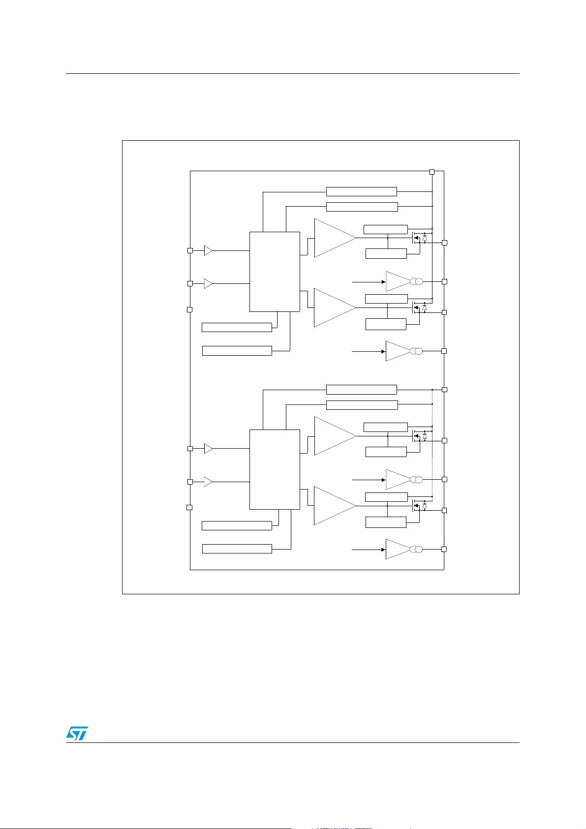
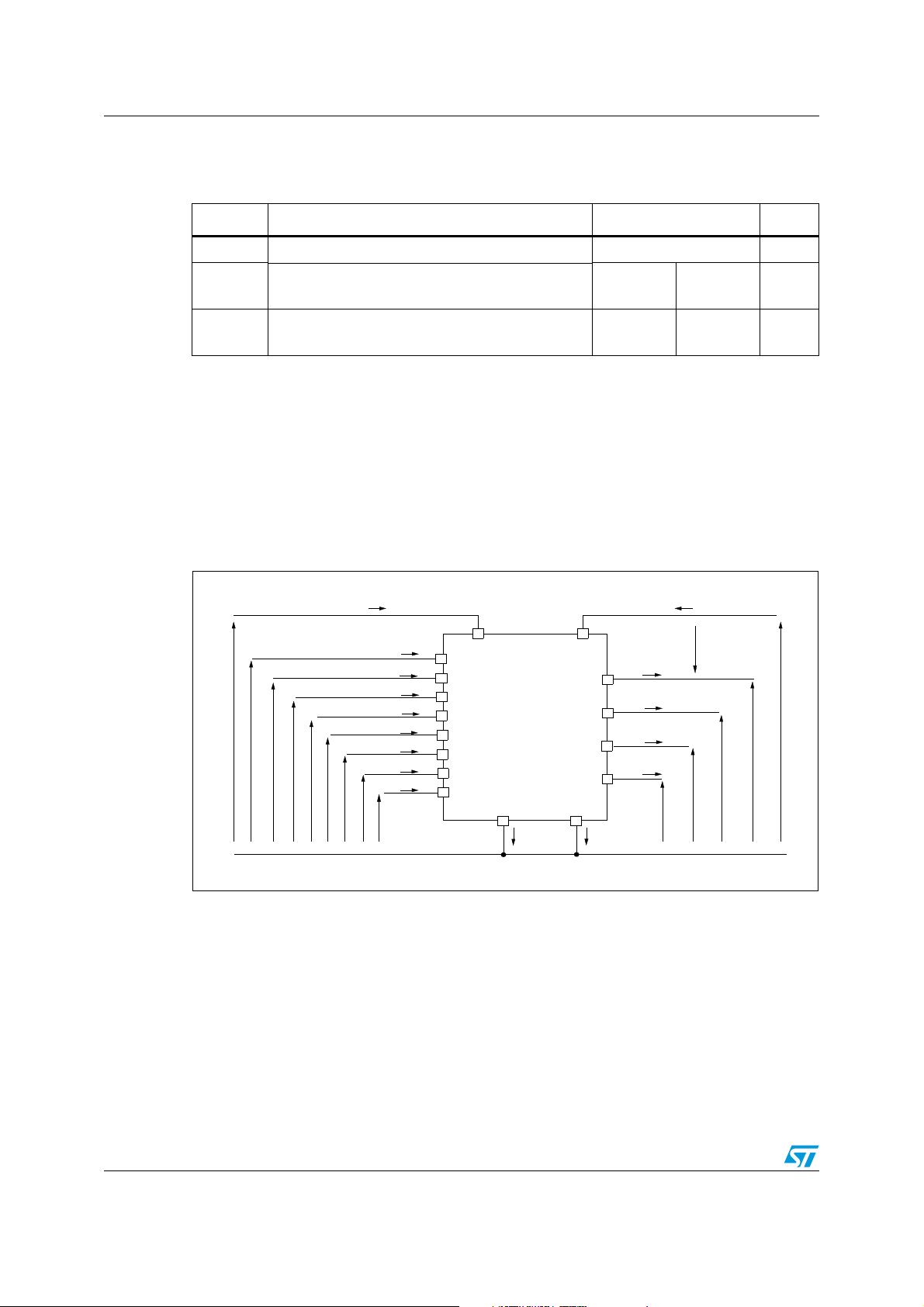
VNQ600 Block diagram and pin description
1 Block diagram and pin description
Figure 1. Block diagram
1,2
V
CC
OVERVOLTAGE
UNDERVOLTAGE
INPUT 1
INPUT 2
GND 1,2
INPUT 3
INPUT 4
GND 3,4
OVERTEMP. 1
OVERTEMP. 2
OVERTEMP. 3
OVERTEMP. 4
LOGIC
LOGIC
DRIVER 1
I
OUT1
DRIVER 2
I
OUT2
OVERVOLTAGE
UNDERVOLTAGE
DRIVER 3
I
OUT3
DRIVER 4
I
OUT4
DEMAG 1
I
LIM1
K
DEMAG 2
I
LIM2
K
DEMAG 3
I
LIM3
K
DEMAG 4
I
LIM4
K
OUTPUT 1
CURRENT
SENSE 1
OUTPUT 2
CURRENT
SENSE 2
V
3,4
CC
OUTPUT 3
CURRENT
SENSE 3
OUTPUT 4
CURRENT
SENSE 4
5/26
Block diagram and pin description VNQ600
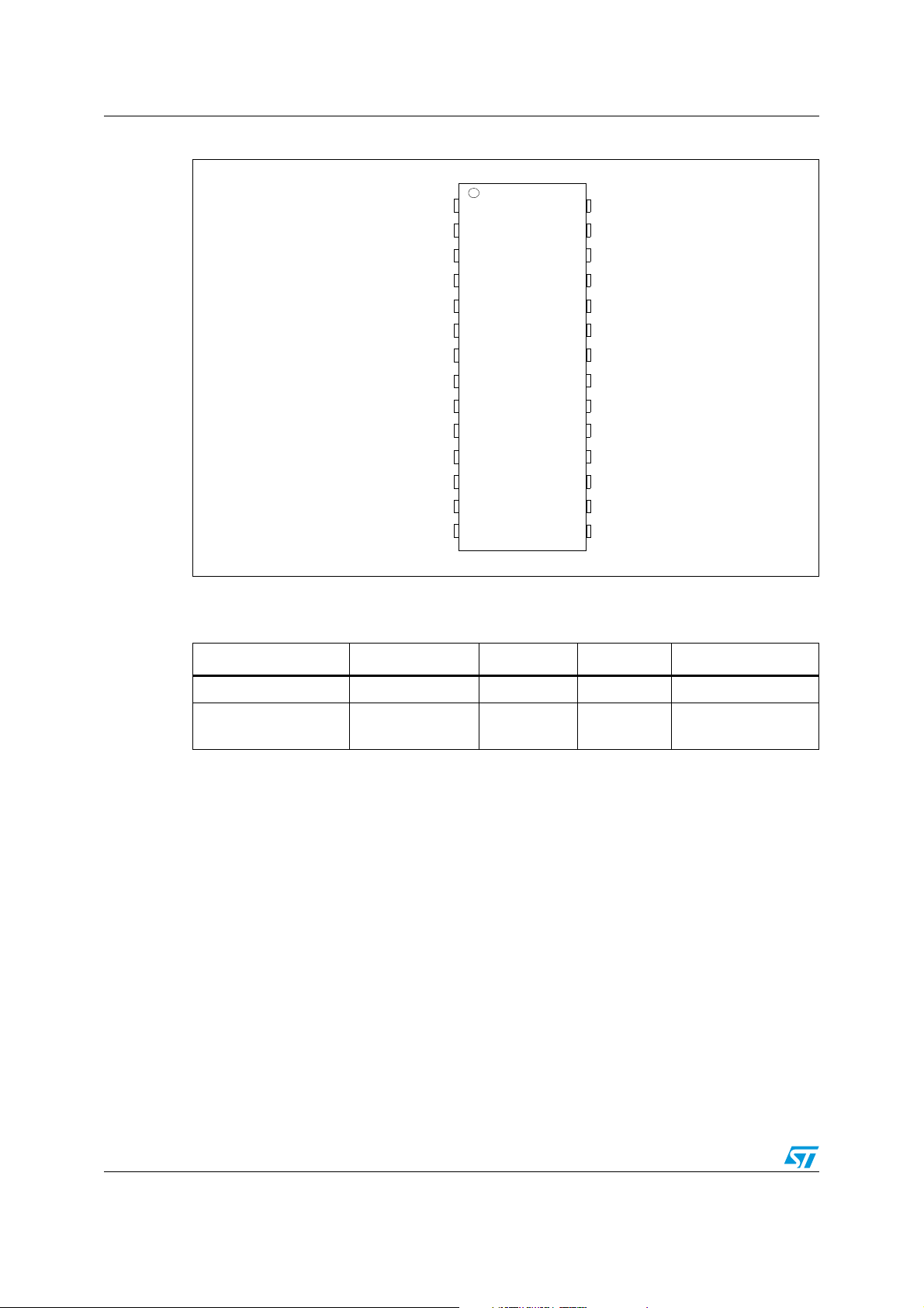
Figure 2. Configuration diagram (top view)
15
28
V
1,2
CC
OUTPUT 2
OUTPUT 2
OUTPUT 2
OUTPUT 1
OUTPUT 1
OUTPUT 1
OUTPUT 4
OUTPUT 4
OUTPUT 4
OUTPUT 3
OUTPUT 3
OUTPUT 3
3,4
V
CC
VCC1,2
1
GND 1,2
INPUT2
INPUT1
CURRENT
CURRENT
SENSE 1
SENSE 2
V
1,2
CC
3,4
V
CC
GND 3,4
INPUT4
INPUT3
CURRENT SENSE 3
CURRENT SENSE 4
V
3,4
CC
Table 2. Suggested connections for unused and not connected pins
14
Connection / pin Current sense N.C. Output Input
Floating X X X
To ground
Through 1KΩ
resistor
X
Through 10KΩ
resistor
6/26
VNQ600 Electrical specifications
2 Electrical specifications
2.1 Absolute maximum ratings
Stressing the device above the rating listed in the “Absolute maximum ratings” table may
cause permanent damage to the device. These are stress ratings only and operation of the
device at these or any other conditions above those indicated in the Operating sections of
this specification is not implied. Exposure to Absolute Maximum Rating conditions for
extended periods may affect device reliability. Refer also to the STMicroelectronics SURE
Program and other relevant quality document.
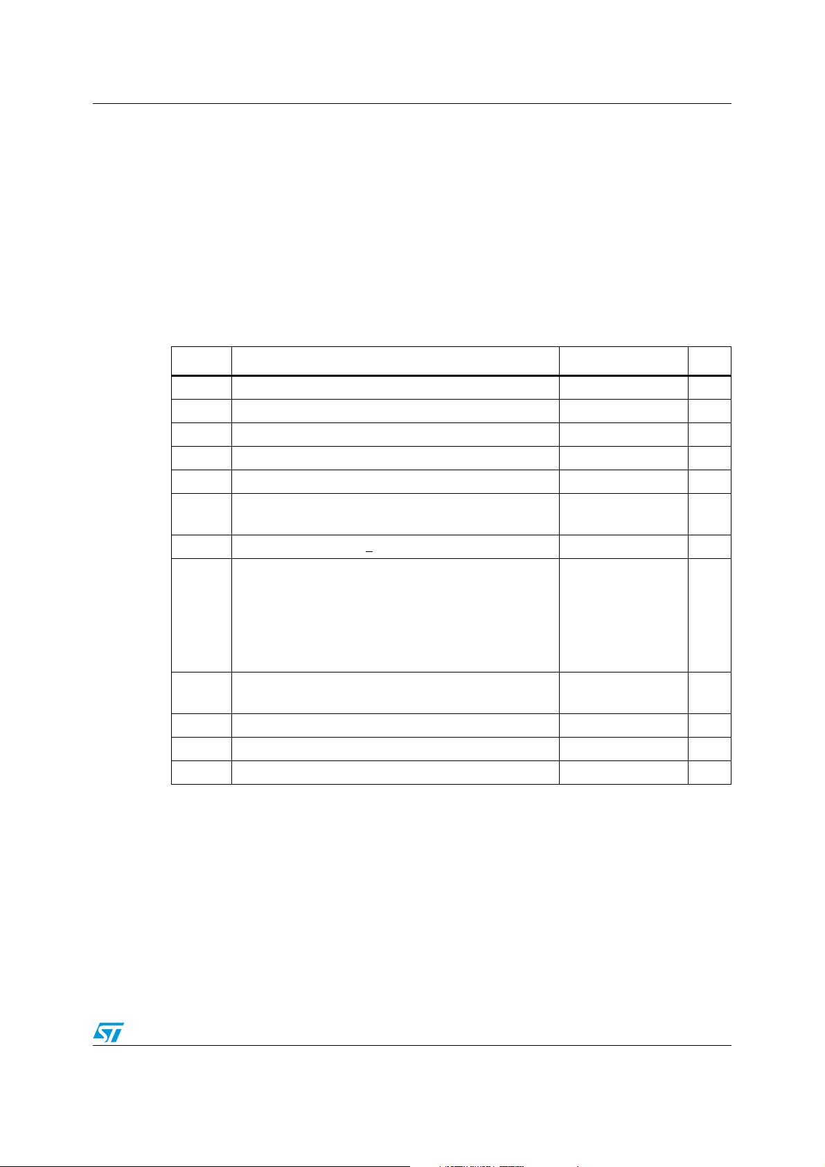
Table 3. Absolute maximum rating
Symbol Parameter Value Unit
V
-V
I
OUT
I
I
V
CSENSE
I
GND
V
ESD
E
MAX
P
T
T
Supply voltage (continuous) 41 V
CC
Reverse supply voltage (continuous) -0.3 V
CC
Output current (continuous), for each channel 15 A
Reverse output current (continuous), for each channel -15 A
R
Input current +/- 10 mA
IN
Current sense maximum voltage
Ground current at T
< 25 °C (continuous) -200 mA
pins
-3
+15
Electrostatic discharge
(Human Body Model: R=1.5KΩ; C=100pF)
- INPUT
- CURRENT SENSE
- OUTPUT
- V
CC
Maximum switching energy
(L=0.11mH; R
Power dissipation (per island) at T
tot
Junction operating temperature Internally limited °C
j
Storage temperature -55 to 150 °C
stg
=0Ω; V
L
=13.5V; T
bat
=150ºC; IL=40A)
jstart
=25°C 6.25 W
lead
4000
2000
5000
5000
126 mJ
V
V
V
V
V
V
7/26
Electrical specifications VNQ600
2.2 Thermal data
Table 4. Thermal data (per island)
Symbol Parameter Value Unit
R
thj-lead
R
thj-amb
R
thj-amb
Thermal resistance junction-lead 20 °C/W
Thermal resistance junction-ambient
(one chip ON)
Thermal Resistance junction-ambient
(two chips ON)
1. When mounted on a standard single-sided FR-4 board with 0.5cm2 of Cu (at least 35 µm thick) connected
to all V
2. When mounted on a standard single-sided FR-4 board with 6cm2 of Cu (at least 35 µm thick) connected to
all V
pins. Horizontal mounting and no artificial air flow.
CC
pins. Horizontal mounting and no artificial air flow.
CC
2.3 Electrical characteristics
Values specified in this section are for 8V<VCC<36V; -40°C< Tj <150°C, unless otherwise
stated.
Figure 3. Current and voltage conventions
I
S3,4
V
CC3,4
I
IN1
V
SENSE3
I
SENSE1
I
IN2
I
SENSE2
I
IN3
I
SENSE3
I
IN4
I
SENSE4
V
IN4
V
STAT4
V
IN1
V
SENSE1
V
IN2
V
SENSE2
V
IN3
V
CC3,4
INPUT1
CUR. SENSE1
INPUT2
CUR. SENSE2
INPUT3
CUR. SENSE3
INPUT4
CUR. SENSE4
GND
3,4
I
GND3,4
V
CC1,2
OUTPUT1
OUTPUT2
OUTPUT3
OUTPUT4
GND
(1)
60
(1)
46
V
F1
I
OUT1
I
OUT2
I
OUT3
V
OUT3
I
OUT4
V
OUT4
1,2
I
GND1,2
I
V
S1,2
OUT2
45
31
(2)
(2)
V
OUT1
V
°C/W
°C/W
CC1,2
Note: V
Fn
= V
CCn
- V
during reverse battery condition.
OUTn
8/26
 Loading...