

Features
VNN7NV04P-E, VNS7NV04P-E
OMNIFET II
fully autoprotected Power MOSFET
Typ e R
VNN7NV04P-E
VNS7NV04P-E
■ Linear current limitation
■ Thermal shutdown
■ Short circuit protection
■ Integrated clamp
■ Low current drawn from input pin
■ Diagnostic feedback through input pin
■ ESD protection
■ Direct access to the gate of the Power
DS(on)
60 mΩ 6A 40V
I
lim
V
clamp
MOSFET (analog driving)
■ Compatible with standard Power MOSFET in
compliance with the 2002/95/EC European
Directive
2
3
2
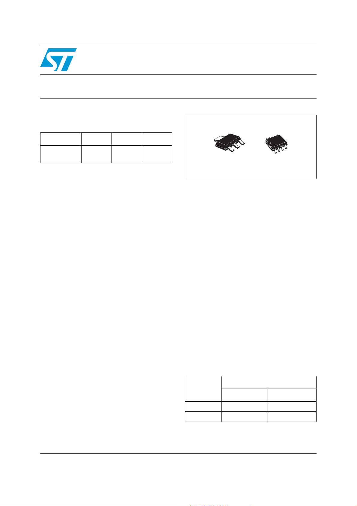
SOT-223
1
SO-8
Description
The VNN7NV04P-E, VNS7NV04P-E, are
monolithic devices designed in
STMicroelectronics VIPower™ M0-3 Technology,
intended for replacement of standard Power
MOSFETs from DC up to 50 kHz applications.
Built in thermal shutdown, linear current limitation
and overvoltage clamp protect the chip in harsh
environments.
Fault feedback can be detected by monitoring the
voltage at the input pin.
Table 1. Device summary
Order codes
Package
Tube Tape and reel
SOT-223 - VNN7NV04PTR-E
SO-8 VNS7NV04P-E VNS7NV04PTR-E
July 2011 Doc ID 15632 Rev 3 1/29
www.st.com
1

Contents VNN7NV04P-E, VNS7NV04P-E
Contents
1 Block diagram and pin description . . . . . . . . . . . . . . . . . . . . . . . . . . . . . 5
2 Electrical specifications . . . . . . . . . . . . . . . . . . . . . . . . . . . . . . . . . . . . . . 6
2.1 Absolute maximum ratings . . . . . . . . . . . . . . . . . . . . . . . . . . . . . . . . . . . . . 6
2.2 Thermal data . . . . . . . . . . . . . . . . . . . . . . . . . . . . . . . . . . . . . . . . . . . . . . . 7
2.3 Electrical characteristics . . . . . . . . . . . . . . . . . . . . . . . . . . . . . . . . . . . . . . . 7
3 Protection features . . . . . . . . . . . . . . . . . . . . . . . . . . . . . . . . . . . . . . . . . . 9
3.1 Electrical characteristics curves . . . . . . . . . . . . . . . . . . . . . . . . . . . . . . . . 12
3.2 SO-8 maximum demagnetization energy . . . . . . . . . . . . . . . . . . . . . . . . . 16
3.3 SOT-223 maximum demagnetization energy . . . . . . . . . . . . . . . . . . . . . . 17
4 Package and PCB thermal data . . . . . . . . . . . . . . . . . . . . . . . . . . . . . . . 18
4.1 SO-8 thermal data . . . . . . . . . . . . . . . . . . . . . . . . . . . . . . . . . . . . . . . . . . 18
4.2 SOT-223 thermal data . . . . . . . . . . . . . . . . . . . . . . . . . . . . . . . . . . . . . . . 20
5 Package and packing information . . . . . . . . . . . . . . . . . . . . . . . . . . . . . 23
5.1 SOT-223 mechanical data . . . . . . . . . . . . . . . . . . . . . . . . . . . . . . . . . . . . 23
5.2 SO-8 mechanical data . . . . . . . . . . . . . . . . . . . . . . . . . . . . . . . . . . . . . . . 24
5.3 SOT-223 packing information . . . . . . . . . . . . . . . . . . . . . . . . . . . . . . . . . . 26
5.4 SO-8 packing information . . . . . . . . . . . . . . . . . . . . . . . . . . . . . . . . . . . . . 27
6 Revision history . . . . . . . . . . . . . . . . . . . . . . . . . . . . . . . . . . . . . . . . . . . 28
2/29 Doc ID 15632 Rev 3

VNN7NV04P-E, VNS7NV04P-E List of tables
List of tables
Table 1. Device summary . . . . . . . . . . . . . . . . . . . . . . . . . . . . . . . . . . . . . . . . . . . . . . . . . . . . . . . . . . 1
Table 2. Absolute maximum ratings . . . . . . . . . . . . . . . . . . . . . . . . . . . . . . . . . . . . . . . . . . . . . . . . . . 6
Table 3. Thermal data. . . . . . . . . . . . . . . . . . . . . . . . . . . . . . . . . . . . . . . . . . . . . . . . . . . . . . . . . . . . . 7
Table 4. Electrical characteristics . . . . . . . . . . . . . . . . . . . . . . . . . . . . . . . . . . . . . . . . . . . . . . . . . . . . 7
Table 5. SO-8 thermal parameter . . . . . . . . . . . . . . . . . . . . . . . . . . . . . . . . . . . . . . . . . . . . . . . . . . . 19
Table 6. SOT-223 thermal parameter . . . . . . . . . . . . . . . . . . . . . . . . . . . . . . . . . . . . . . . . . . . . . . . . 22
Table 7. SOT-223 mechanical data . . . . . . . . . . . . . . . . . . . . . . . . . . . . . . . . . . . . . . . . . . . . . . . . . 23
Table 8. SO-8 mechanical data . . . . . . . . . . . . . . . . . . . . . . . . . . . . . . . . . . . . . . . . . . . . . . . . . . . . 24
Table 9. Document revision history . . . . . . . . . . . . . . . . . . . . . . . . . . . . . . . . . . . . . . . . . . . . . . . . . 28
Doc ID 15632 Rev 3 3/29

List of figures VNN7NV04P-E, VNS7NV04P-E
List of figures
Figure 1. Block diagram . . . . . . . . . . . . . . . . . . . . . . . . . . . . . . . . . . . . . . . . . . . . . . . . . . . . . . . . . . . . 5
Figure 2. Configuration diagram (top view) . . . . . . . . . . . . . . . . . . . . . . . . . . . . . . . . . . . . . . . . . . . . . 5
Figure 3. Current and voltage conventions . . . . . . . . . . . . . . . . . . . . . . . . . . . . . . . . . . . . . . . . . . . . . 6
Figure 4. Switching time test circuit for resistive load . . . . . . . . . . . . . . . . . . . . . . . . . . . . . . . . . . . . 10
Figure 5. Test circuit for diode recovery times . . . . . . . . . . . . . . . . . . . . . . . . . . . . . . . . . . . . . . . . . . 10
Figure 6. Unclamped inductive load test circuits . . . . . . . . . . . . . . . . . . . . . . . . . . . . . . . . . . . . . . . . 11
Figure 7. Input charge test circuit. . . . . . . . . . . . . . . . . . . . . . . . . . . . . . . . . . . . . . . . . . . . . . . . . . . . 11
Figure 8. Unclamped inductive waveforms . . . . . . . . . . . . . . . . . . . . . . . . . . . . . . . . . . . . . . . . . . . . 11
Figure 9. Derating curve . . . . . . . . . . . . . . . . . . . . . . . . . . . . . . . . . . . . . . . . . . . . . . . . . . . . . . . . . . 12
Figure 10. Transconductance . . . . . . . . . . . . . . . . . . . . . . . . . . . . . . . . . . . . . . . . . . . . . . . . . . . . . . . 12
Figure 11. Static drain-source on resistance vs input voltage (part 1/2) . . . . . . . . . . . . . . . . . . . . . . . 12
Figure 12. Static drain-source on resistance vs input voltage (part 2/2) . . . . . . . . . . . . . . . . . . . . . . . 12
Figure 13. Source-drain diode forward characteristics . . . . . . . . . . . . . . . . . . . . . . . . . . . . . . . . . . . . 12
Figure 14. Static drain source on resistance . . . . . . . . . . . . . . . . . . . . . . . . . . . . . . . . . . . . . . . . . . . . 12
Figure 15. Turn-on current slope (part 1/2) . . . . . . . . . . . . . . . . . . . . . . . . . . . . . . . . . . . . . . . . . . . . . 13
Figure 16. Turn-on current slope (part 2/2) . . . . . . . . . . . . . . . . . . . . . . . . . . . . . . . . . . . . . . . . . . . . . 13
Figure 17. Transfer characteristics . . . . . . . . . . . . . . . . . . . . . . . . . . . . . . . . . . . . . . . . . . . . . . . . . . . 13
Figure 18. Static drain-source on resistance vs Id . . . . . . . . . . . . . . . . . . . . . . . . . . . . . . . . . . . . . . . . 13
Figure 19. Input voltage vs input charge . . . . . . . . . . . . . . . . . . . . . . . . . . . . . . . . . . . . . . . . . . . . . . . 13
Figure 20. Turn-off drain source voltage slope (part 1/2). . . . . . . . . . . . . . . . . . . . . . . . . . . . . . . . . . . 13
Figure 21. Turn-off drain source voltage slope (part 2/2). . . . . . . . . . . . . . . . . . . . . . . . . . . . . . . . . . . 14
Figure 22. Capacitance variations . . . . . . . . . . . . . . . . . . . . . . . . . . . . . . . . . . . . . . . . . . . . . . . . . . . . 14
Figure 23. Output characteristics . . . . . . . . . . . . . . . . . . . . . . . . . . . . . . . . . . . . . . . . . . . . . . . . . . . . . 14
Figure 24. Normalized on resistance vs temperature . . . . . . . . . . . . . . . . . . . . . . . . . . . . . . . . . . . . . 14
Figure 25. Switching time resistive load (part 1/2) . . . . . . . . . . . . . . . . . . . . . . . . . . . . . . . . . . . . . . . . 14
Figure 26. Switching time resistive load (part 2/2) . . . . . . . . . . . . . . . . . . . . . . . . . . . . . . . . . . . . . . . . 14
Figure 27. Normalized input threshold voltage vs temperature . . . . . . . . . . . . . . . . . . . . . . . . . . . . . . 15
Figure 28. Normalized current limit vs junction temperature . . . . . . . . . . . . . . . . . . . . . . . . . . . . . . . . 15
Figure 29. Step response current limit . . . . . . . . . . . . . . . . . . . . . . . . . . . . . . . . . . . . . . . . . . . . . . . . . 15
Figure 30. SO-8 maximum turn-off current versus load inductance. . . . . . . . . . . . . . . . . . . . . . . . . . . 16
Figure 31. SO-8 demagnetization . . . . . . . . . . . . . . . . . . . . . . . . . . . . . . . . . . . . . . . . . . . . . . . . . . . . 16
Figure 32. SOT-223 maximum turn-off current versus load inductance . . . . . . . . . . . . . . . . . . . . . . . 17
Figure 33. SOT-223 demagnetization . . . . . . . . . . . . . . . . . . . . . . . . . . . . . . . . . . . . . . . . . . . . . . . . . 17
Figure 34. SO-8 PC board . . . . . . . . . . . . . . . . . . . . . . . . . . . . . . . . . . . . . . . . . . . . . . . . . . . . . . . . . . 18
Figure 35. Rthj-amb vs PCB copper area in open box free air condition. . . . . . . . . . . . . . . . . . . . . . . 18
Figure 36. SO-8 thermal impedance junction ambient single pulse. . . . . . . . . . . . . . . . . . . . . . . . . . . 19
Figure 37. Thermal fitting model of an OMNIFET II in SO-8 . . . . . . . . . . . . . . . . . . . . . . . . . . . . . . . . 19
Figure 38. SOT-223 PC board . . . . . . . . . . . . . . . . . . . . . . . . . . . . . . . . . . . . . . . . . . . . . . . . . . . . . . . 20
Figure 39. Rthj-amb vs PCB copper area in open box free air condition. . . . . . . . . . . . . . . . . . . . . . . 20
Figure 40. SOT-223 thermal impedance junction ambient single pulse. . . . . . . . . . . . . . . . . . . . . . . . 21
Figure 41. Thermal fitting model of an OMNIFET II in SOT-223 . . . . . . . . . . . . . . . . . . . . . . . . . . . . . 21
Figure 42. SOT-223 package dimensions . . . . . . . . . . . . . . . . . . . . . . . . . . . . . . . . . . . . . . . . . . . . . . 23
Figure 43. SO-8 package dimensions . . . . . . . . . . . . . . . . . . . . . . . . . . . . . . . . . . . . . . . . . . . . . . . . . 25
Figure 44. SOT-223 tape and reel shipment (suffix “TR”) . . . . . . . . . . . . . . . . . . . . . . . . . . . . . . . . . . 26
Figure 45. SO-8 tube shipment (no suffix) . . . . . . . . . . . . . . . . . . . . . . . . . . . . . . . . . . . . . . . . . . . . . . 27
Figure 46. SO-8 tape and reel shipment (suffix “TR”) . . . . . . . . . . . . . . . . . . . . . . . . . . . . . . . . . . . . . 27
4/29 Doc ID 15632 Rev 3

VNN7NV04P-E, VNS7NV04P-E Block diagram and pin description
1 Block diagram and pin description
Figure 1. Block diagram
DRAIN
2
Overvoltage
Clamp
INPUT
1
Gate
Control
Over
Temperature
Current
Limiter
Figure 2. Configuration diagram (top view)
SO-8 Package
SOURCE
SOURCE
SOURCE
INPUT
1
4
1. For the pins configuration related to SOT-223 see outlines at page 1.
(1)
8
5
Linear
DRAIN
DRAIN
DRAIN
DRAIN
3
SOURCE
FC01000
Doc ID 15632 Rev 3 5/29

Electrical specifications VNN7NV04P-E, VNS7NV04P-E
2 Electrical specifications
Figure 3. Current and voltage conventions
I
D
V
DS
I
IN
R
IN
INPUT
V
IN
2.1 Absolute maximum ratings
DRAIN
SOURCE
Table 2. Absolute maximum ratings
Value
Symbol Parameter
Unit
SOT-223 SO-8
V
V
R
IN MIN
V
ESD1
V
ESD2
P
DS
IN
I
IN
I
D
I
R
tot
Drain-source voltage (VIN= 0 V) Internally clamped V
Input voltage Internally clamped V
Input current +/-20 mA
Minimum input series impedance 150 Ω
Drain current Internally limited A
Reverse DC output current -10.5 A
Electrostatic discharge (R = 1.5 KΩ,
C = 100 pF)
Electrostatic discharge on output pin only
(R = 330 Ω, C = 150 pF)
4000 V
16500 V
Total dissipation at Tc=25°C 7 4.6 W
Maximum switching energy (L = 0.7 mH;
E
MAX
R
L
=9A)
I
L
=0Ω; V
=13.5V; T
bat
jstart
=150°C;
40 mJ
Maximum switching energy (L = 0.6 mH;
E
MAX
T
T
T
j
c
stg
R
L
=9A)
I
L
=0Ω; V
=13.5V; T
bat
jstart
=150°C;
Operating junction temperature Internally limited °C
Case operating temperature Internally limited °C
Storage temperature -55 to 150 °C
37 mJ
6/29 Doc ID 15632 Rev 3

VNN7NV04P-E, VNS7NV04P-E Electrical specifications
2.2 Thermal data
Table 3. Thermal data
Val ue
Symbol Parameter
SOT-223 SO-8
Unit
R
thj-case
R
thj-lead
R
thj-amb
1. When mounted on a standard single-sided FR4 board with 0.5 mm2 of Cu (at least 35 µm thick) connected
to all DRAIN pins.
Thermal resistance junction-case max 18 °C/W
Thermal resistance junction-lead max 27 °C/W
Thermal resistance junction-ambient max 96
(1)
90
(1)
2.3 Electrical characteristics
-40 °C < Tj < 150 °C, unless otherwise specified.
Table 4. Electrical characteristics
Symbol Parameter Test conditions Min Typ Max Unit
Off
V
CLAMP
V
CLTH
V
INTH
I
ISS
Drain-source clamp
voltage
Drain-source clamp
threshold voltage
=0V; ID= 3.5 A 40 45 55 V
V
IN
=0V; ID=2mA 36 V
V
IN
Input threshold voltage VDS=VIN; ID=1mA 0.5 2.5 V
Supply current from input
pin
=0V; VIN= 5 V 100 150 µA
V
DS
°C/W
V
INCL
I
DSS
On
R
DS(on)
Dynamic (T
(1)
g
fs
C
OSS
I
=1mA 6 6.8 8 V
Input-source clamp
voltage
Zero input voltage drain
current (V
=0V)
IN
Static drain-source on
resistance
= 25 °C, unless otherwise specified)
j
Forward
transconductance
IN
IIN= -1 mA -1.0 -0.3 V
V
=13V; VIN=0V; Tj=25°C 30 µA
DS
V
=25V; VIN= 0 V 75 µA
DS
=5V; ID= 3.5 A; Tj=25°C 65 mΩ
V
IN
V
=5V; ID= 3.5 A 130 mΩ
IN
V
=13V; ID=3.5A 9 S
DD
Output capacitance VDS=13V; f=1MHz; VIN=0V 220 pF
Doc ID 15632 Rev 3 7/29

Electrical specifications VNN7NV04P-E, VNS7NV04P-E
Table 4. Electrical characteristics (continued)
Symbol Parameter Test conditions Min Typ Max Unit
Switching (Tj= 25 °C, unless otherwise specified)
t
d(on)
t
t
d(off)
t
t
d(on)
t
t
d(off)
t
(dI/dt)
Q
Tu r n- on d el ay t im e
=15V; ID=3.5A;
V
Rise time 470 1500 ns
r
Turn-off delay time 500 1500 ns
Fall time 350 1000 ns
f
DD
V
=5V; R
gen
gen=RIN MIN
(see figure Figure 4)
=150Ω;
Tu r n- on d el ay t im e
=15V; ID=3.5A;
V
Rise time 4.6 14.0 µs
r
Turn-off delay time 5.4 16.0 µs
Fall time 3.6 11.0 µs
f
Turn-on current slope
on
Total input charge
i
DD
V
gen
=5V; R
=2.2KΩ;
gen
(see figure Figure 4)
=15V; ID= 3.5 A; V
V
DD
R
gen=RIN MIN
=12V; ID= 3.5 A; VIN=5V;
V
DD
I
= 2.13 mA (see figure Figure 7)
gen
=150Ω
gen
=5V;
100 300 ns
0.75 2.3 µs
6.5 A/µs
18 nC
Source drain diode (Tj= 25 °C, unless otherwise specified)
(1)
V
SD
t
Qrr Reverse recovery charge 0.28 µC
I
RRM
Protections (-40 °C < T
I
lim
t
dlim
Forward on voltage ISD= 3.5 A; VIN=0V 0.8 V
Reverse recovery time
rr
ISD= 3.5 A; dI/dt = 20 A/µs;
220 ns
VDD= 30 V; L = 200 µH;
Reverse recovery current 2.5 A
< 150 °C, unless otherwise specified)
j
(see test circuit, figure Figure 5)
Drain current limit VIN=5V; VDS=13V 6 9 12 A
Step response current
limit
=5V; VDS=13V 4.0 µs
V
IN
T
jsh
T
I
E
1. Pulsed: Pulse duration = 300 µs, duty cycle 1.5 %
Overtemperature
shutdown
Overtemperature reset 135 °C
jrs
Fault sink current VIN=5V; VDS=13V; Tj=T
gf
Single pulse avalanche
as
energy
starting T
R
gen=RIN MIN
(see Figure 6 and Figure 8)
=25°C; VDD=24V; VIN=5V;
j
8/29 Doc ID 15632 Rev 3
jsh
=150Ω; L = 24 mH;
150 175 200 °C
15 mA
200 mJ

VNN7NV04P-E, VNS7NV04P-E Protection features
3 Protection features
During normal operation, the input pin is electrically connected to the gate of the internal
Power MOSFET through a low impedance path.
The device then behaves like a standard Power MOSFET and can be used as a switch from
DC up to 50 kHz. The only difference from the user’s standpoint is that a small DC current
I
(typ. 100µA) flows into the input pin in order to supply the internal circuitry.
ISS
The device integrates:
● Overvoltage clamp protection: internally set at 45 V, along with the rugged avalanche
characteristics of the Power MOSFET stage give this device unrivalled ruggedness and
energy handling capability. This feature is mainly important when driving inductive
loads.
● Linear current limiter circuit: limits the drain current I
voltages. When the current limiter is active, the device operates in the linear region, so
power dissipation may exceed the capability of the heatsink. Both case and junction
temperatures increase, and if this phase lasts long enough, junction temperature may
reach the overtemperature threshold T
● Overtemperature and short circuit protection: these are based on sensing the chip
jsh
.
temperature and are not dependent on the input voltage. The location of the sensing
element on the chip in the power stage area ensures fast, accurate detection of the
junction temperature. Overtemperature cutout occurs in the range 150 to 190 °C, a
typical value being 170 °C. The device is automatically restarted when the chip
temperature falls of about 15 °C below shutdown temperature.
● Status feedback: in the case of an overtemperature fault condition (T
tries to sink a diagnostic current I
through the input pin in order to indicate fault
gf
condition. If driven from a low impedance source, this current may be used in order to
warn the control circuit of a device shutdown. If the drive impedance is high enough so
that the input pin driver is not able to supply the current I
however not affects the device operation: no requirement is put on the current capability
of the input pin driver except to be able to supply the normal operation drive current
I
.
ISS
Additional features of this device are ESD protection according to the Human Body model
and the ability to be driven from a TTL logic circuit.
to I
D
whatever the input pin
lim
> T
), the device
j
jsh
, the input pin falls to 0 V. This
gf
Doc ID 15632 Rev 3 9/29
 Loading...