

Features
VND1NV04
VNN1NV04 - VNS1NV04
OMNIFET II
fully autoprotected Power MOSFET
Parameter Symbol Value
Max on-state resistance (per ch.) R
Current limitation (typ) I
Drain-source clamp voltage V
■ Linear current limitation
■ Thermal shutdown
■ Short circuit protection
■ Integrated clamp
■ Low current drawn from input pin
■ Diagnostic feedback through input pin
■ ESD protection
■ Direct access to the gate of the Power
LIMH
CLAMP
ON
250 mΩ
1.7 A
40 V
MOSFET (analog driving)
■ Compatible with standard Power MOSFET
3
1
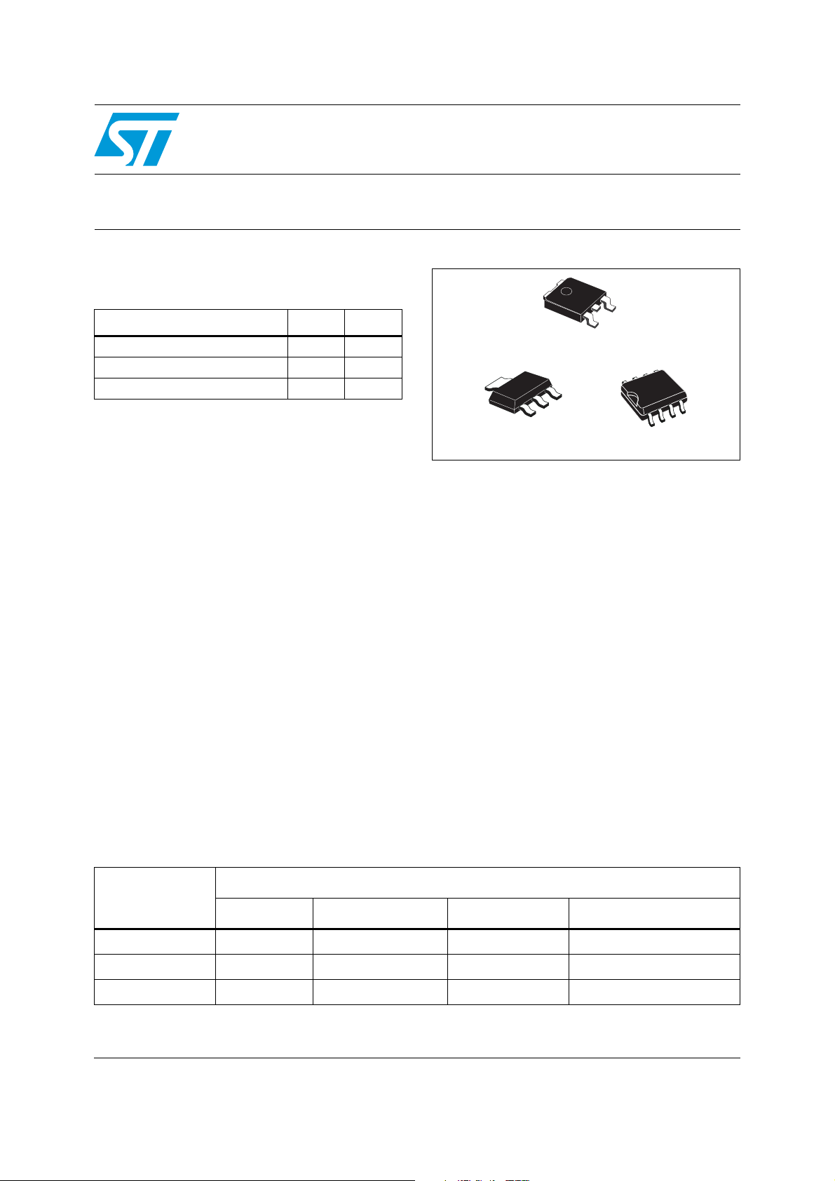
TO-252 (DPAK)
2
3
2
1
SOT-223
SO-8
Description
The VND1NV04, VNN1NV04, VNS1NV04 are
monolithic devices designed in
STMicroelectronics
intended for replacement of standard Power
MOSFETs from DC up to 50 KHz applications.
Built in thermal shutdown, linear current limitation
and overvoltage clamp protect the chip in harsh
environments.
Fault feedback can be detected by monitoring the
voltage at the input pin.
®
VIPower® M0-3 Technology,
Table 1. Device summary
Order codes
Package
Tube Tube (lead free) Tape and reel Tape and reel (lead free)
TO-252 (DPAK) VND1NV04 VND1NV04-E VND1NV0413TR VND1NV04TR-E
SOT-223 VNN1NV04 - VNN1NV0413TR -
SO-8 VNS1NV04 - VNS1NV0413TR -
December 2011 Doc ID 7381 Rev 3 1/33
www.st.com
1

Contents VND1NV04 - VNN1NV04 - VNS1NV04
Contents
1 Block diagram and pin description . . . . . . . . . . . . . . . . . . . . . . . . . . . . . 5
2 Electrical specifications . . . . . . . . . . . . . . . . . . . . . . . . . . . . . . . . . . . . . . 6
2.1 Absolute maximum ratings . . . . . . . . . . . . . . . . . . . . . . . . . . . . . . . . . . . . . 6
2.2 Thermal data . . . . . . . . . . . . . . . . . . . . . . . . . . . . . . . . . . . . . . . . . . . . . . . 7
2.3 Electrical characteristics . . . . . . . . . . . . . . . . . . . . . . . . . . . . . . . . . . . . . . . 7
2.4 Electrical characteristics curves . . . . . . . . . . . . . . . . . . . . . . . . . . . . . . . . 12
3 Protection features . . . . . . . . . . . . . . . . . . . . . . . . . . . . . . . . . . . . . . . . . 16
4 Package and PCB thermal data . . . . . . . . . . . . . . . . . . . . . . . . . . . . . . . 17
4.1 DPAK thermal data . . . . . . . . . . . . . . . . . . . . . . . . . . . . . . . . . . . . . . . . . . 17
4.2 SOT-223 thermal data . . . . . . . . . . . . . . . . . . . . . . . . . . . . . . . . . . . . . . . 19
4.3 SO-8 thermal data . . . . . . . . . . . . . . . . . . . . . . . . . . . . . . . . . . . . . . . . . . 22
5 Package and packing information . . . . . . . . . . . . . . . . . . . . . . . . . . . . . 25
5.1 DPAK mechanical data . . . . . . . . . . . . . . . . . . . . . . . . . . . . . . . . . . . . . . . 25
5.2 SOT-223 mechanical data . . . . . . . . . . . . . . . . . . . . . . . . . . . . . . . . . . . . 27
5.3 SO8 mechanical data . . . . . . . . . . . . . . . . . . . . . . . . . . . . . . . . . . . . . . . . 27
5.4 DPAK packing information . . . . . . . . . . . . . . . . . . . . . . . . . . . . . . . . . . . . 29
5.5 SOT-223 packing information . . . . . . . . . . . . . . . . . . . . . . . . . . . . . . . . . . 30
5.6 SO8 packing information . . . . . . . . . . . . . . . . . . . . . . . . . . . . . . . . . . . . . 31
6 Revision history . . . . . . . . . . . . . . . . . . . . . . . . . . . . . . . . . . . . . . . . . . . 32
2/33 Doc ID 7381 Rev 3

VND1NV04 - VNN1NV04 - VNS1NV04 List of tables
List of tables
Table 1. Device summary . . . . . . . . . . . . . . . . . . . . . . . . . . . . . . . . . . . . . . . . . . . . . . . . . . . . . . . . . . 1
Table 2. Absolute maximum ratings . . . . . . . . . . . . . . . . . . . . . . . . . . . . . . . . . . . . . . . . . . . . . . . . . . 6
Table 3. Thermal data. . . . . . . . . . . . . . . . . . . . . . . . . . . . . . . . . . . . . . . . . . . . . . . . . . . . . . . . . . . . . 7
Table 4. Electrical characteristics . . . . . . . . . . . . . . . . . . . . . . . . . . . . . . . . . . . . . . . . . . . . . . . . . . . . 7
Table 5. DPAK thermal parameter . . . . . . . . . . . . . . . . . . . . . . . . . . . . . . . . . . . . . . . . . . . . . . . . . . 19
Table 6. SOT-223 thermal parameter . . . . . . . . . . . . . . . . . . . . . . . . . . . . . . . . . . . . . . . . . . . . . . . . 21
Table 7. SO-8 thermal parameter . . . . . . . . . . . . . . . . . . . . . . . . . . . . . . . . . . . . . . . . . . . . . . . . . . . 24
Table 8. DPAK mechanical data . . . . . . . . . . . . . . . . . . . . . . . . . . . . . . . . . . . . . . . . . . . . . . . . . . . . 26
Table 9. SO-8 mechanical data . . . . . . . . . . . . . . . . . . . . . . . . . . . . . . . . . . . . . . . . . . . . . . . . . . . . 27
Table 10. Document revision history . . . . . . . . . . . . . . . . . . . . . . . . . . . . . . . . . . . . . . . . . . . . . . . . . 32
Doc ID 7381 Rev 3 3/33

List of figures VND1NV04 - VNN1NV04 - VNS1NV04
List of figures
Figure 1. Block diagram . . . . . . . . . . . . . . . . . . . . . . . . . . . . . . . . . . . . . . . . . . . . . . . . . . . . . . . . . . . . 5
Figure 2. Configuration diagram (top view) . . . . . . . . . . . . . . . . . . . . . . . . . . . . . . . . . . . . . . . . . . . . . 5
Figure 3. Current and voltage conventions . . . . . . . . . . . . . . . . . . . . . . . . . . . . . . . . . . . . . . . . . . . . . 6
Figure 4. Switching time test circuit for resistive load . . . . . . . . . . . . . . . . . . . . . . . . . . . . . . . . . . . . . 9
Figure 5. Test circuit for diode recovery times . . . . . . . . . . . . . . . . . . . . . . . . . . . . . . . . . . . . . . . . . . 10
Figure 6. Unclamped inductive load test circuits . . . . . . . . . . . . . . . . . . . . . . . . . . . . . . . . . . . . . . . . 10
Figure 7. Input charge test circuit. . . . . . . . . . . . . . . . . . . . . . . . . . . . . . . . . . . . . . . . . . . . . . . . . . . . 11
Figure 8. Unclamped inductive waveforms . . . . . . . . . . . . . . . . . . . . . . . . . . . . . . . . . . . . . . . . . . . . 11
Figure 9. Source-drain diode forward characteristics . . . . . . . . . . . . . . . . . . . . . . . . . . . . . . . . . . . . 12
Figure 10. Static drain-source on resistance . . . . . . . . . . . . . . . . . . . . . . . . . . . . . . . . . . . . . . . . . . . . 12
Figure 11. Derating curve . . . . . . . . . . . . . . . . . . . . . . . . . . . . . . . . . . . . . . . . . . . . . . . . . . . . . . . . . . 12
Figure 12. Static drain-source on resistance vs. input voltage (part 1/2) . . . . . . . . . . . . . . . . . . . . . . . 12
Figure 13. Static drain-source on resistance vs. input voltage (part 2/2) . . . . . . . . . . . . . . . . . . . . . . . 12
Figure 14. Transconductance . . . . . . . . . . . . . . . . . . . . . . . . . . . . . . . . . . . . . . . . . . . . . . . . . . . . . . . 12
Figure 15. Static drain-source on resistance vs. Id . . . . . . . . . . . . . . . . . . . . . . . . . . . . . . . . . . . . . . . 13
Figure 16. Transfer characteristics . . . . . . . . . . . . . . . . . . . . . . . . . . . . . . . . . . . . . . . . . . . . . . . . . . . 13
Figure 17. Turn-on current slope (part 1/2) . . . . . . . . . . . . . . . . . . . . . . . . . . . . . . . . . . . . . . . . . . . . . 13
Figure 18. Turn-on current slope (part 2/2) . . . . . . . . . . . . . . . . . . . . . . . . . . . . . . . . . . . . . . . . . . . . . 13
Figure 19. Input voltage vs. input charge . . . . . . . . . . . . . . . . . . . . . . . . . . . . . . . . . . . . . . . . . . . . . . . 13
Figure 20. Turn-off drain source voltage slope (part 1/2). . . . . . . . . . . . . . . . . . . . . . . . . . . . . . . . . . . 13
Figure 21. Turn-off drain-source voltage slope (part 2/2) . . . . . . . . . . . . . . . . . . . . . . . . . . . . . . . . . . 14
Figure 22. Capacitance variations . . . . . . . . . . . . . . . . . . . . . . . . . . . . . . . . . . . . . . . . . . . . . . . . . . . . 14
Figure 23. Switching time resistive load (part 1/2) . . . . . . . . . . . . . . . . . . . . . . . . . . . . . . . . . . . . . . . . 14
Figure 24. Switching time resistive load (part 2/2) . . . . . . . . . . . . . . . . . . . . . . . . . . . . . . . . . . . . . . . . 14
Figure 25. Output characteristics . . . . . . . . . . . . . . . . . . . . . . . . . . . . . . . . . . . . . . . . . . . . . . . . . . . . . 14
Figure 26. Normalized on resistance vs. temperature . . . . . . . . . . . . . . . . . . . . . . . . . . . . . . . . . . . . . 14
Figure 27. Normalized input threshold voltage vs. temperature . . . . . . . . . . . . . . . . . . . . . . . . . . . . . 15
Figure 28. Normalized current limit vs. junction temperature. . . . . . . . . . . . . . . . . . . . . . . . . . . . . . . . 15
Figure 29. Step response current limit . . . . . . . . . . . . . . . . . . . . . . . . . . . . . . . . . . . . . . . . . . . . . . . . . 15
Figure 30. DPAK PC board . . . . . . . . . . . . . . . . . . . . . . . . . . . . . . . . . . . . . . . . . . . . . . . . . . . . . . . . . 17
Figure 31. DPAK Rthj-amb vs. PCB copper area in open box free air condition. . . . . . . . . . . . . . . . . 17
Figure 32. DPAK thermal impedance junction ambient single pulse . . . . . . . . . . . . . . . . . . . . . . . . . . 18
Figure 33. DPAK thermal fitting model of a single channel . . . . . . . . . . . . . . . . . . . . . . . . . . . . . . . . . 18
Figure 34. SOT-223 PC board . . . . . . . . . . . . . . . . . . . . . . . . . . . . . . . . . . . . . . . . . . . . . . . . . . . . . . . 19
Figure 35. SOT-223 Rthj-amb vs. PCB copper area in open box free air condition . . . . . . . . . . . . . . 20
Figure 36. SOT-223 thermal impedance junction ambient single pulse . . . . . . . . . . . . . . . . . . . . . . . 20
Figure 37. SOT-223 thermal fitting model of a single channel . . . . . . . . . . . . . . . . . . . . . . . . . . . . . . 21
Figure 38. SO-8 PC board . . . . . . . . . . . . . . . . . . . . . . . . . . . . . . . . . . . . . . . . . . . . . . . . . . . . . . . . . . 22
Figure 39. SO-8 Rthj-amb vs. PCB copper area in open box free air condition . . . . . . . . . . . . . . . . . 22
Figure 40. SO-8 thermal impedance junction ambient single pulse . . . . . . . . . . . . . . . . . . . . . . . . . . 23
Figure 41. SO-8 thermal fitting model of a single channel . . . . . . . . . . . . . . . . . . . . . . . . . . . . . . . . . 23
Figure 42. DPAK package dimensions . . . . . . . . . . . . . . . . . . . . . . . . . . . . . . . . . . . . . . . . . . . . . . . . 25
Figure 43. SOT-223 mechanical data & package outline . . . . . . . . . . . . . . . . . . . . . . . . . . . . . . . . . . 27
Figure 44. SO-8 package dimension . . . . . . . . . . . . . . . . . . . . . . . . . . . . . . . . . . . . . . . . . . . . . . . . . . 28
Figure 45. SOT-223 tape and reel shipment (suffix “TR”) . . . . . . . . . . . . . . . . . . . . . . . . . . . . . . . . . . 30
Figure 46. SO-8 tube shipment (no suffix) . . . . . . . . . . . . . . . . . . . . . . . . . . . . . . . . . . . . . . . . . . . . . . 31
Figure 47. SO-8 tape and reel shipment (suffix “TR”) . . . . . . . . . . . . . . . . . . . . . . . . . . . . . . . . . . . . . 31
4/33 Doc ID 7381 Rev 3
VND1NV04 - VNN1NV04 - VNS1NV04 Block diagram and pin description
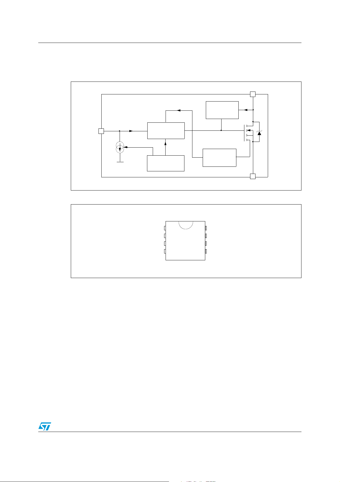
1 Block diagram and pin description
Figure 1. Block diagram
DRAIN
2
Overvoltage
Clamp
INPUT
1
Gate
Control
Over
Temperature
Linear
Current
Limiter
Figure 2. Configuration diagram (top view)
SOURCE
1
8
SOURCE
SOURCE
INPUT
1. For the pins configuration related to SOT-223 and DPAK see outline at page 1.
4
5
DRAIN
DRAIN
DRAIN
DRAIN
3
SOURCE
Doc ID 7381 Rev 3 5/33
Electrical specifications VND1NV04 - VNN1NV04 - VNS1NV04
2 Electrical specifications
Figure 3. Current and voltage conventions
I
D
V
DS
R
I
IN
IN
INPUT
V
IN
2.1 Absolute maximum ratings
DRAIN
SOURCE
The rating listed in Table 2: Absolute maximum ratings may cause permanent damage to
the device. These are stress ratings only and operation of the device at these or any other
conditions above those indicated in the operating sections of this specification is not implied.
Exposure to Absolute maximum rating conditions for extended periods may affect device
reliability.
Table 2. Absolute maximum ratings
Symbol Parameter
V
V
I
R
IN MINn
V
ESD1
V
ESD2
P
T
Drain-source voltage (V
DSn
Input voltage Internally clamped V
INn
Input current +/-20 mA
INn
=0 V) Internally clamped V
INn
Minimum input series impedance 330 Ω
Drain current Internally limited A
I
Dn
I
Reverse DC output current -3 A
Rn
Electrostatic discharge (R=1.5 KΩ, C=100 pF) 4000 V
Electrostatic discharge on output pins only
(R=330 Ω, C=150 pF)
Total dissipation at Tc=25 °C 7 8.3 35 W
tot
T
Operating junction temperature Internally limited °C
j
T
Case operating temperature Internally limited °C
c
Storage temperature -55 to 150 °C
stg
SOT-223 SO-8 DPAK
Value
Unit
16500 V
6/33 Doc ID 7381 Rev 3
VND1NV04 - VNN1NV04 - VNS1NV04 Electrical specifications
2.2 Thermal data
Table 3. Thermal data
Maximum value
Symbol Parameter
SOT-223 SO-8 DPAK
Unit
R
thj-case
R
thj-lead
R
thj-amb
1. When mounted on a standard single-sided FR4 board with 50 mm2 of Cu (at least 35 μm thick) connected
to all DRAIN pins
Thermal resistance junction-case 18 3.5 °C/W
Thermal resistance junction-lead 15 °C/W
Thermal resistance junction-ambient 70
2.3 Electrical characteristics
Table 4. Electrical characteristics
Symbol Parameter Test conditions Min. Typ. Max. Unit
Off (-40 °C<Tj<150 °C, unless otherwise specified)
V
CLAMP
V
CLTH
V
INTH
I
V
INCL
I
DSS
On (-40 °C<Tj<150 °C, unless otherwise specified)
Drain-source clamp
voltage
Drain-source clamp
threshold voltage
Input threshold
voltage
Supply current from
ISS
input pin
Input-source clamp
voltage
Zero input voltage
drain current
(V
IN
=0 V)
=0 V; ID=0.5 A 40 45 55 V
V
IN
=0 V; ID=2 mA 36 V
V
IN
V
DS=VIN
=0 V; VIN=5 V 100 150 µA
V
DS
I
=1 mA 6 6.8 8 V
IN
I
=-1 mA -1.0 -0.3
IN
V
=13 V; VIN=0 V; Tj=25 °C 30 µA
DS
=25 V; VIN=0 V 75
V
DS
(1)
65
(1)
54
(1)
°C/W
; ID=1 mA 0.5 2.5 V
R
DS(on)
Dynamic (T
(1)
g
fs
C
OSS
=5 V; ID=0.5 A; Tj=25 °C 250 mΩ
V
Static drain-source on
resistance
=25 °C, unless otherwise specified)
j
Forward
transconductance
IN
V
=5 V; ID=0.5 A 500
IN
V
=13 V; ID=0.5 A 2 S
DD
Output capacitance VDS=13 V; f=1 MHz; VIN=0 V 90 pF
Doc ID 7381 Rev 3 7/33
Electrical specifications VND1NV04 - VNN1NV04 - VNS1NV04
Table 4. Electrical characteristics (continued)
Symbol Parameter Test conditions Min. Typ. Max. Unit
Switching (T
t
d(on)
t
r
t
d(off)
t
f
t
d(on)
t
r
t
d(off)
t
f
(dI/dt)
on
Q
i
=25 °C, unless otherwise specified)
j
Turn-on delay time
Rise time 170 500 ns
Turn-off delay time 350 1000 ns
Fall time 200 600 ns
Turn-on delay time
Rise time 1.3 4.0 µs
Turn-off delay time 1.8 5.5 µs
Fall time 1.2 4.0 µs
Turn-on current slope
Total input charge
Source drain diode (T
(1)
V
SD
Qrr
I
RRM
Forward on voltage ISD=0.5 A; VIN=0 V 0.8 V
Reverse recovery
t
rr
time
Reverse recovery
charge
Reverse recovery
current
V
=15 V; ID=0.5 A
DD
V
gen
=5 V; R
gen=RIN MIN
=330 Ω
(see Figure 4)
=15 V; ID=0.5 A
V
DD
V
gen
=5 V; R
=2.2 KΩ
gen
(see Figure 4)
VDD=15 V; ID=1.5 A
=5 V; R
V
gen
V
=12 V; ID=0.5 A; VIN=5 V
DD
=2.13 mA (see Figure 7)
I
gen
=25 °C, unless otherwise specified)
j
I
=0.5 A; dI/dt=6 A/µs
SD
=30V; L=200µH
V
DD
gen=RIN MIN
=330 Ω
(see Figure 5)
70 200 ns
0.25 1.0 µs
5A/µs
5nC
205 ns
100 nC
0.7 A
Protections (-40 °C<Tj<150 °C, unless otherwise specified)
I
t
dlim
T
T
Drain current limit VIN=5 V; VDS=13 V 1.7 3.5 A
lim
Step response
current limit
Overtemperature
jsh
shutdown
Overtemperature
jrs
reset
Fault sink current VIN=5 V; VDS=13 V; Tj=T
I
gf
VIN=5 V; VDS=13 V 2.0 µs
Starting Tj=25 °C; VDD=24 V
Single pulse
E
as
avalanche energy
=5 V R
V
IN
L=50 mH
gen=RIN MIN
(see Figure 6 and Figure 8)
1. Pulsed: pulse duration = 300 µs, duty cycle 1.5 %
8/33 Doc ID 7381 Rev 3
jsh
=330 Ω;
150 175 200 °C
135 °C
10 15 20 mA
55 mJ
VND1NV04 - VNN1NV04 - VNS1NV04 Electrical specifications
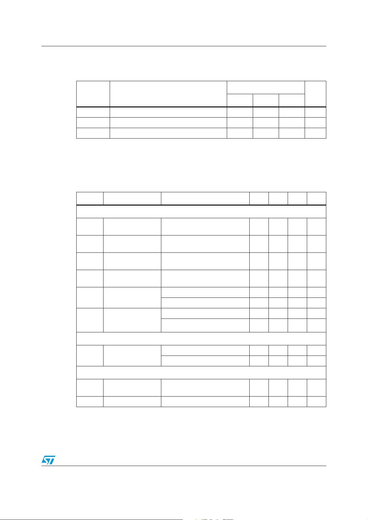
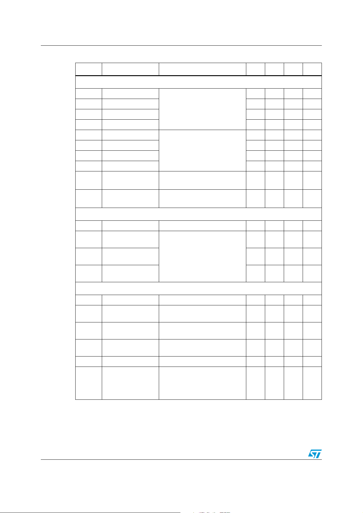
Figure 4.
Switching time test circuit for resistive load
R
V
gen
I
D
90%
t
d(off)
t
f
t
r
t
V
gen
d(on)
10%
V
gen
D
t
t
Doc ID 7381 Rev 3 9/33
Electrical specifications VND1NV04 - VNN1NV04 - VNS1NV04
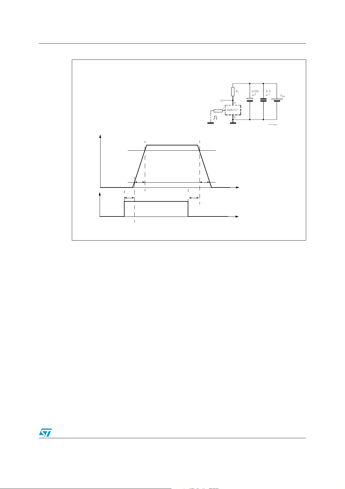
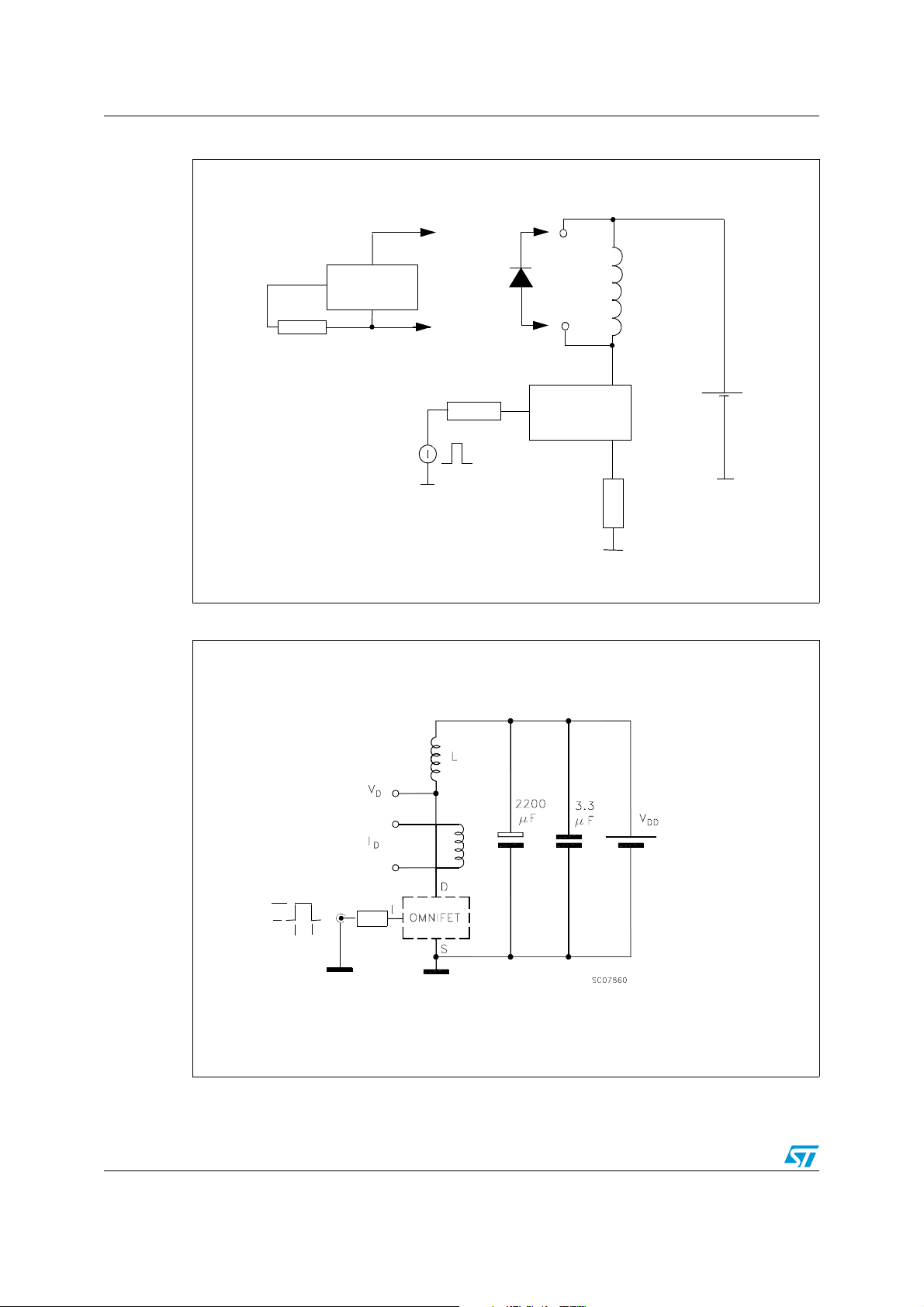
Figure 5.
Test circuit for diode recovery times
A
D
330
I
OMNIFET
Ω
S
V
gen
FAS T
DIODE
B
R
gen
I
A
B
OMNIFET
L=100uH
D
S
8.5
V
DD
Ω
Figure 6. Unclamped inductive load test circuits
R
V
IN
P
W
GEN
10/33 Doc ID 7381 Rev 3
 Loading...