

Features
Type V
VNL5160N3-E
VNL5160S5-E
clamp
41 V 160 mΩ 3.5 A
R
DS(on)
I
D
VNL5160N3-E
VNL5160S5-E
OMNIFET III
fully protected low-side driver
2
3
2
1
SOT-223
SO-8
■ Drain current:3.5A
■ ESD protection
■ Overvoltage clamp
■ Thermal shutdown
■ Current and power limitation
■ Very low standby current
■ Very low electromagnetic susceptibility
■ In compliance with the 2002/95/EC European
directive
■ Open drain status output
Specially intended for R10W or 2x R5W
■
(a)
automotive signal lamps
Description
The VNL5160N3-E and VNL5160S5-E are
monolithic devices, made using
STMicroelectronics
intended for driving resistive or inductive loads
with one side connected to the battery. Built-in
thermal shutdown protects the chip from
overtemperature and short circuit. Output current
limitation protects the devices in an overload
condition. In the case of a long duration overload,
the device limits the dissipated power to a safe
level up to thermal shutdown intervention.
Thermal shutdown, with automatic restart, allows
the device to recover normal operation as soon as
a fault condition disappears. Fast
demagnetization of inductive loads is achieved at
turn-off.
®
VIPower® Tec h n o l o gy,
a. Valid for VNL5160S5-E only.
Table 1. Device summary
Order codes
Package
Tube Tape and reel
SOT-223 VNL5160N3-E VNL5160N3TR-E
SO-8 VNL5160S5-E VNL5160S5TR-E
February 2012 Doc ID 16364 Rev 2 1/26
www.st.com
1

Contents VNL5160N3-E, VNL5160S5-E
Contents
1 Block diagrams and pins configurations . . . . . . . . . . . . . . . . . . . . . . . . 5
2 Absolute maximum rating . . . . . . . . . . . . . . . . . . . . . . . . . . . . . . . . . . . . 8
2.1 Absolute maximum ratings . . . . . . . . . . . . . . . . . . . . . . . . . . . . . . . . . . . . . 8
2.2 Thermal data . . . . . . . . . . . . . . . . . . . . . . . . . . . . . . . . . . . . . . . . . . . . . . . 9
3 Electrical characteristics . . . . . . . . . . . . . . . . . . . . . . . . . . . . . . . . . . . . 10
4 Application information . . . . . . . . . . . . . . . . . . . . . . . . . . . . . . . . . . . . . 14
4.1 MCU I/O protection . . . . . . . . . . . . . . . . . . . . . . . . . . . . . . . . . . . . . . . . . . 15
5 Package and PC board thermal data . . . . . . . . . . . . . . . . . . . . . . . . . . . 16
5.1 SOT-223 thermal data . . . . . . . . . . . . . . . . . . . . . . . . . . . . . . . . . . . . . . . 16
5.2 SO-8 thermal data . . . . . . . . . . . . . . . . . . . . . . . . . . . . . . . . . . . . . . . . . . 18
6 Package and packing information . . . . . . . . . . . . . . . . . . . . . . . . . . . . . 21
6.1 ECOPACK® packages . . . . . . . . . . . . . . . . . . . . . . . . . . . . . . . . . . . . . . . 21
6.2 SOT-223 mechanical data . . . . . . . . . . . . . . . . . . . . . . . . . . . . . . . . . . . . 21
6.3 SO8 mechanical data . . . . . . . . . . . . . . . . . . . . . . . . . . . . . . . . . . . . . . . . 22
6.4 SOT-223 packing information . . . . . . . . . . . . . . . . . . . . . . . . . . . . . . . . . . 23
6.5 SO8 packing information . . . . . . . . . . . . . . . . . . . . . . . . . . . . . . . . . . . . . 24
7 Revision history . . . . . . . . . . . . . . . . . . . . . . . . . . . . . . . . . . . . . . . . . . . 25
2/26 Doc ID 16364 Rev 2

VNL5160N3-E, VNL5160S5-E List of tables
List of tables
Table 1. Device summary . . . . . . . . . . . . . . . . . . . . . . . . . . . . . . . . . . . . . . . . . . . . . . . . . . . . . . . . . . 1
Table 2. Pin function . . . . . . . . . . . . . . . . . . . . . . . . . . . . . . . . . . . . . . . . . . . . . . . . . . . . . . . . . . . . . . 6
Table 3. Suggested connections for unused and not connected pins . . . . . . . . . . . . . . . . . . . . . . . . 7
Table 4. Absolute maximum ratings . . . . . . . . . . . . . . . . . . . . . . . . . . . . . . . . . . . . . . . . . . . . . . . . . . 8
Table 5. Thermal data. . . . . . . . . . . . . . . . . . . . . . . . . . . . . . . . . . . . . . . . . . . . . . . . . . . . . . . . . . . . . 9
Table 6. PowerMOS section . . . . . . . . . . . . . . . . . . . . . . . . . . . . . . . . . . . . . . . . . . . . . . . . . . . . . . . 10
Table 7. Source drain diode . . . . . . . . . . . . . . . . . . . . . . . . . . . . . . . . . . . . . . . . . . . . . . . . . . . . . . . 10
Table 8. Input section . . . . . . . . . . . . . . . . . . . . . . . . . . . . . . . . . . . . . . . . . . . . . . . . . . . . . . . . . . . . 10
Table 9. Status pin . . . . . . . . . . . . . . . . . . . . . . . . . . . . . . . . . . . . . . . . . . . . . . . . . . . . . . . . . . . . . . 11
Table 10. Logic input . . . . . . . . . . . . . . . . . . . . . . . . . . . . . . . . . . . . . . . . . . . . . . . . . . . . . . . . . . . . . 11
Table 11. Openload detection. . . . . . . . . . . . . . . . . . . . . . . . . . . . . . . . . . . . . . . . . . . . . . . . . . . . . . . 11
Table 12. Supply section . . . . . . . . . . . . . . . . . . . . . . . . . . . . . . . . . . . . . . . . . . . . . . . . . . . . . . . . . . 11
Table 13. Switching characteristics (Vcc=13V). . . . . . . . . . . . . . . . . . . . . . . . . . . . . . . . . . . . . . . . . . 12
Table 14. Protection and diagnostics . . . . . . . . . . . . . . . . . . . . . . . . . . . . . . . . . . . . . . . . . . . . . . . . . 12
Table 15. Truth table . . . . . . . . . . . . . . . . . . . . . . . . . . . . . . . . . . . . . . . . . . . . . . . . . . . . . . . . . . . . . 13
Table 16. SOT-223 thermal parameter . . . . . . . . . . . . . . . . . . . . . . . . . . . . . . . . . . . . . . . . . . . . . . . . 17
Table 17. SO-8 thermal parameter . . . . . . . . . . . . . . . . . . . . . . . . . . . . . . . . . . . . . . . . . . . . . . . . . . . 20
Table 18. Document revision history . . . . . . . . . . . . . . . . . . . . . . . . . . . . . . . . . . . . . . . . . . . . . . . . . 25
Doc ID 16364 Rev 2 3/26

List of figures VNL5160N3-E, VNL5160S5-E
List of figures
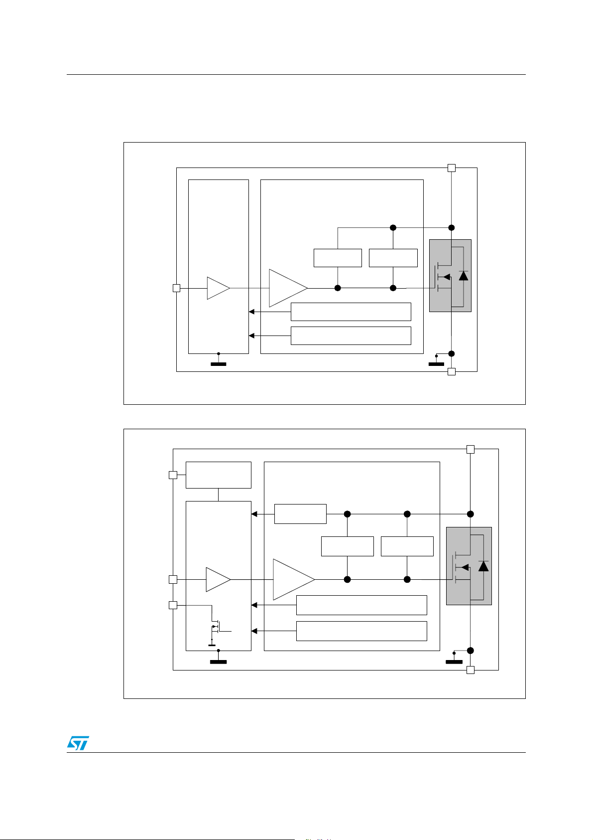
Figure 1. VNL5160N3-E block diagram . . . . . . . . . . . . . . . . . . . . . . . . . . . . . . . . . . . . . . . . . . . . . . . . 5
Figure 2. VNL5160S5-E block diagram . . . . . . . . . . . . . . . . . . . . . . . . . . . . . . . . . . . . . . . . . . . . . . . 5
Figure 3. VNL5160N3-E current and voltage conventions. . . . . . . . . . . . . . . . . . . . . . . . . . . . . . . . . . 6
Figure 4. VNL5160S5-E current and voltage conventions . . . . . . . . . . . . . . . . . . . . . . . . . . . . . . . . . 6
Figure 5. Configuration diagrams (top view) . . . . . . . . . . . . . . . . . . . . . . . . . . . . . . . . . . . . . . . . . . . . 7
Figure 6. Switching characteristics . . . . . . . . . . . . . . . . . . . . . . . . . . . . . . . . . . . . . . . . . . . . . . . . . . 13
Figure 7. VNL5160N3-E application schematic . . . . . . . . . . . . . . . . . . . . . . . . . . . . . . . . . . . . . . . . . 14
Figure 8. VNL5160S5-E application schematic . . . . . . . . . . . . . . . . . . . . . . . . . . . . . . . . . . . . . . . . . 14
Figure 9. Maximum demagnetization energy. . . . . . . . . . . . . . . . . . . . . . . . . . . . . . . . . . . . . . . . . . . 15
Figure 10. SOT-223 PC board . . . . . . . . . . . . . . . . . . . . . . . . . . . . . . . . . . . . . . . . . . . . . . . . . . . . . . . 16
Figure 11. SOT-223 Rthj-amb vs PCB copper area in open box free air condition . . . . . . . . . . . . . . . 16
Figure 12. SOT-223 thermal impedance junction ambient single pulse . . . . . . . . . . . . . . . . . . . . . . . 17
Figure 13. SOT-223 thermal fitting model
Figure 14. SO-8 PC board . . . . . . . . . . . . . . . . . . . . . . . . . . . . . . . . . . . . . . . . . . . . . . . . . . . . . . . . . . 18
Figure 15. SO-8 Rthj-amb vs PCB copper area in open box free air condition . . . . . . . . . . . . . . . . . . 19
Figure 16. SO-8 thermal impedance junction ambient single pulse. . . . . . . . . . . . . . . . . . . . . . . . . . . 19
Figure 17. SO-8 thermal fitting mode
Figure 18. SOT-223 mechanical data & package outline . . . . . . . . . . . . . . . . . . . . . . . . . . . . . . . . . . 21
Figure 19. SO8 mechanical data & package outline . . . . . . . . . . . . . . . . . . . . . . . . . . . . . . . . . . . . . . 22
Figure 20. SOT-223 tape and reel shipment (suffix “TR”) . . . . . . . . . . . . . . . . . . . . . . . . . . . . . . . . . . 23
Figure 21. SO-8 tube shipment (no suffix) . . . . . . . . . . . . . . . . . . . . . . . . . . . . . . . . . . . . . . . . . . . . . . 24
Figure 22. SO-8 tape and reel shipment (suffix “TR”) . . . . . . . . . . . . . . . . . . . . . . . . . . . . . . . . . . . . . 24
(1)
. . . . . . . . . . . . . . . . . . . . . . . . . . . . . . . . . . . . . . . . . . . . 17
(1)
l. . . . . . . . . . . . . . . . . . . . . . . . . . . . . . . . . . . . . . . . . . . . . . . . 20
4/26 Doc ID 16364 Rev 2
VNL5160N3-E, VNL5160S5-E Block diagrams and pins configurations
1 Block diagrams and pins configurations
Figure 1. VNL5160N3-E block diagram
$2!).
#ONTROL$IAGNOSTIC,/')#
).054
$2)6%2
!#4)6%0/7%2,)-)4!4)/.
Figure 2. VNL5160S5-E block diagram
3500,9
6/,4!'%
3500,9
,/')#
#ONTROL$IAGNOSTIC
/&&3TATE
/PENLOAD
#URRENT
,IMITATION
/6%24%-0%2!452%
02/4%#4)/.
/6%2,/!$02/4%#4)/.
#URRENT
,IMITATION
0O WER
#LAMP
0OWER
#LAMP
'.$
("1($'5
$2!).
).054
34!453
$2)6%2
/6%24%-0%2!452%
02/4%#
/6%2,/!$02/4%#4)/.
!#4)6%0/7%2,)-)4!4)/.
4)/.
'.$
("1($'5
Doc ID 16364 Rev 2 5/26
Block diagrams and pins configurations VNL5160N3-E, VNL5160S5-E
Table 2. Pin function
Name Function
INPUT
Voltage controlled input pin with hysteresis, CMOS compatible. Controls output
switch state
(1)
DRAIN PowerMOS drain
SOURCE PowerMOS source and ground reference for the control section
SUPPLY
VOLTAGE
STATUS Open drain digital diagnostic pin
1. Internally connected to V
2. Valid for VNL5160S5-E only.
Supply voltage connected to the signal part (5V)
(2)
in the VNL5160N3-E.
supply
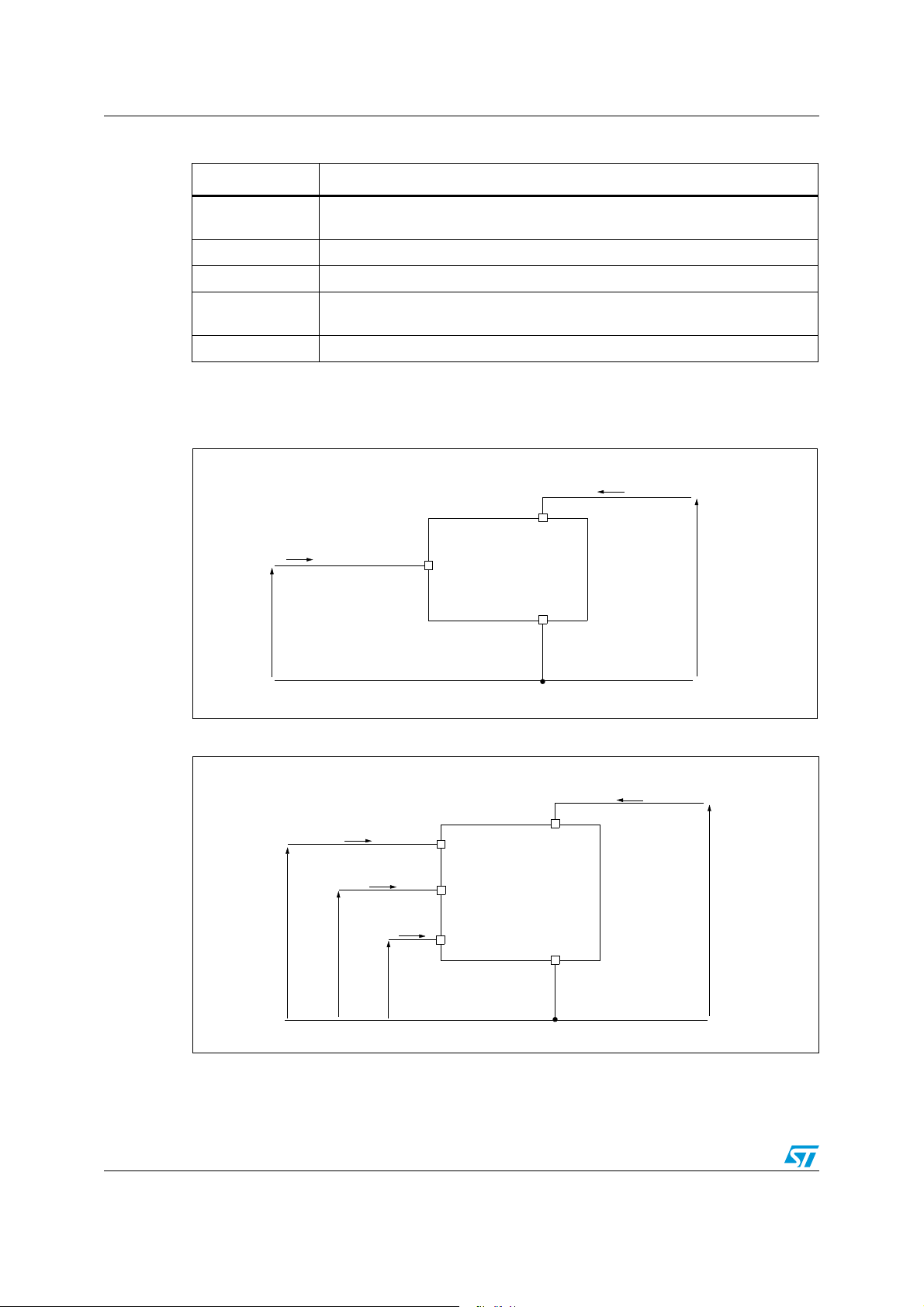
Figure 3. VNL5160N3-E current and voltage conventions
I
D
DRAIN
I
IN
INPUT
SOURCE
V
DS
V
IN
Figure 4. VNL5160S5-E current and voltage conventions
I
IN
I
STAT
V
IN
V
STAT
V
SUPPLY
INPUT
STATUS
I
S
SUPPLY
VOLTAGE
DRAIN
SOURCE
I
D
V
DS
6/26 Doc ID 16364 Rev 2
VNL5160N3-E, VNL5160S5-E Block diagrams and pins configurations
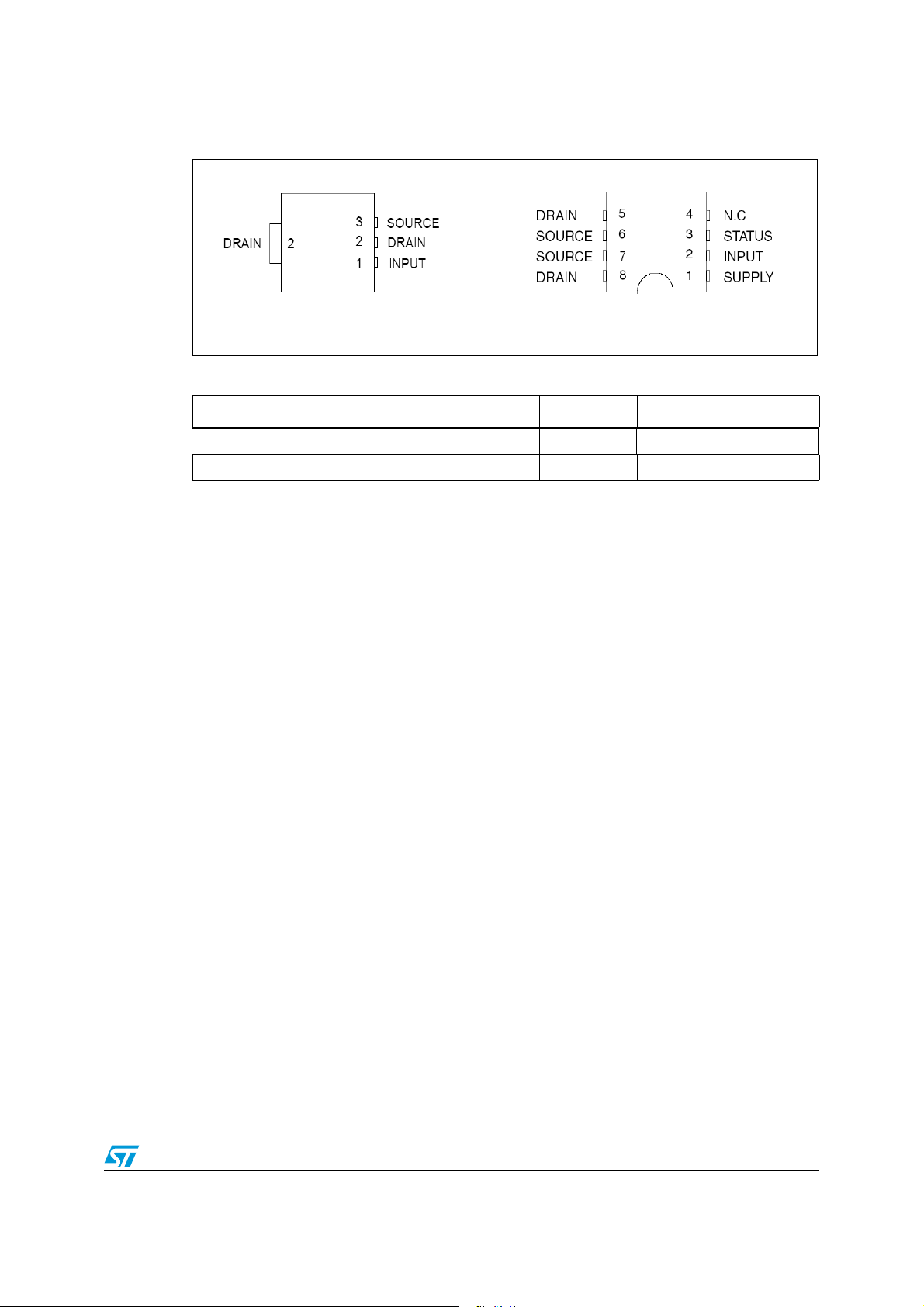
Figure 5. Configuration diagrams (top view)
SOT-223
Table 3. Suggested connections for unused and not connected pins
SO-8
Connection/pin Status N.C. Input
Floating X X X
To ground Not allowed X Through 10kΩ resistor
Doc ID 16364 Rev 2 7/26
Absolute maximum rating VNL5160N3-E, VNL5160S5-E
2 Absolute maximum rating
Stressing the device above the rating listed in Tabl e 4 may cause permanent damage to the
device. These are stress ratings only and operation of the device at these or any other
conditions above those indicated in the Operating sections of this specification is not
implied. Exposure to absolute maximum rating conditions for extended periods may affect
device reliability. Refer also to the STMicroelectronics SURE Program and other relevant
quality document
2.1 Absolute maximum ratings
Table 4. Absolute maximum ratings
Val ue Un it
Symbol Parameter
SOT-223 SO-8
V
- I
I
STAT
V
ESD1
V
ESD2
T
E
Drain-source voltage (VIN=0V) Internally clamped V
DS
DC drain current Internally limited A
I
D
Reverse DC drain current -4 A
D
DC supply current - -1 to 10 mA
I
S
DC input current -1 to 10 mA
I
IN
DC status current - -1 to 10 mA
Electrostatic discharge (R=1.5kΩ; C=100pF)
–INPUT
–STATUS
– SUPPLY
– DRAIN
Electrostatic discharge on output pin only
(R=330Ω, C=150pF)
T
Junction operating temperature -40 to 150 °C
j
Storage temperature -55 to 150 °C
stg
4000
4000
4000
5000
2000 V
Single pulse avalanche energy
L=8.5mH, T
as
V
=13.5V, I
batt
= 150 °C, RL=0Ω,
j
out=IlimL
37 mJ
V
8/26 Doc ID 16364 Rev 2
 Loading...