


Features
VNL5050N3-E
VNL5050S5-E
OMNIFET III
fully protected low-side driver
Typ e V
VNL5050N3-E
VNL5050S5-E
■ Drain current: 19 A
■ ESD protection
■ Overvoltage clamp
■ Thermal shutdown
■ Current and power limitation
■ Very low standby current
■ Very low electromagnetic susceptibility
■ In compliance with the 2002/95/EC european
clamp
41 V 50 mΩ 19 A
R
DS(on)
I
D
directive
■ Open drain status output
(a)
2
3
2
1
SOT-223
SO-8
Description
The VNL5050N3-E and VNL5050S5-E are
monolithic devices made using
STMicroelectronics VIPower Technology,
intended for driving resistive or inductive loads
with one side connected to the battery. Built-in
thermal shutdown protects the chip from
overtemperature and short-circuit. Output current
limitation protects the devices in an overload
condition. In case of long duration overload, the
device limits the dissipated power to a safe level
up to thermal shutdown intervention.Thermal
shutdown, with automatic restart, allows the
device to recover normal operation as soon as a
fault condition disappears. Fast demagnetization
of inductive loads is achieved at turn-off.
a. Valid for VNL5050S5-E only
Table 1. Devices summary
Package
SOT-223 VNL5050N3-E VNL5050N3TR-E
SO-8 VNL5050S5-E VNL5050S5TR-E
November 2009 Doc ID 15917 Rev 4 1/32
Order codes
Tube Tape & reel
www.st.com
1

Contents VNL5050N3-E / VNL5050S5-E
Contents
1 Block diagrams and pins configurations . . . . . . . . . . . . . . . . . . . . . . . . 5
2 Absolute maximum rating . . . . . . . . . . . . . . . . . . . . . . . . . . . . . . . . . . . . 8
2.1 Absolute maximum ratings . . . . . . . . . . . . . . . . . . . . . . . . . . . . . . . . . . . . . 8
2.2 Thermal data . . . . . . . . . . . . . . . . . . . . . . . . . . . . . . . . . . . . . . . . . . . . . . . 8
3 Electrical characteristics . . . . . . . . . . . . . . . . . . . . . . . . . . . . . . . . . . . . . 9
3.1 Electrical characteristics curves . . . . . . . . . . . . . . . . . . . . . . . . . . . . . . . . 12
3.2 MCU I/O protection . . . . . . . . . . . . . . . . . . . . . . . . . . . . . . . . . . . . . . . . . . 17
4 Package and PC board thermal data . . . . . . . . . . . . . . . . . . . . . . . . . . . 18
4.1 SOT-223 thermal data . . . . . . . . . . . . . . . . . . . . . . . . . . . . . . . . . . . . . . . 18
4.2 SO-8 thermal data . . . . . . . . . . . . . . . . . . . . . . . . . . . . . . . . . . . . . . . . . . 21
5 Package and packing information . . . . . . . . . . . . . . . . . . . . . . . . . . . . . 24
5.1 ECOPACK® . . . . . . . . . . . . . . . . . . . . . . . . . . . . . . . . . . . . . . . . . . . . . . . 24
5.2 SOT-223 mechanical data . . . . . . . . . . . . . . . . . . . . . . . . . . . . . . . . . . . . 24
5.3 SO-8 mechanical data . . . . . . . . . . . . . . . . . . . . . . . . . . . . . . . . . . . . . . . 26
5.4 SOT-223 packing information . . . . . . . . . . . . . . . . . . . . . . . . . . . . . . . . . . 28
5.5 SO-8 packing information . . . . . . . . . . . . . . . . . . . . . . . . . . . . . . . . . . . . . 29
6 Revision history . . . . . . . . . . . . . . . . . . . . . . . . . . . . . . . . . . . . . . . . . . . 30
2/32 Doc ID 15917 Rev 4

VNL5050N3-E / VNL5050S5-E List of tables
List of tables
Table 1. Devices summary . . . . . . . . . . . . . . . . . . . . . . . . . . . . . . . . . . . . . . . . . . . . . . . . . . . . . . . . . 1
Table 2. Pin function . . . . . . . . . . . . . . . . . . . . . . . . . . . . . . . . . . . . . . . . . . . . . . . . . . . . . . . . . . . . . . 6
Table 3. Suggested connections for unused and n.c. pins . . . . . . . . . . . . . . . . . . . . . . . . . . . . . . . . . 7
Table 4. Absolute maximum ratings . . . . . . . . . . . . . . . . . . . . . . . . . . . . . . . . . . . . . . . . . . . . . . . . . . 8
Table 5. Thermal data . . . . . . . . . . . . . . . . . . . . . . . . . . . . . . . . . . . . . . . . . . . . . . . . . . . . . . . . . . . . . 8
Table 6. Power MOS section . . . . . . . . . . . . . . . . . . . . . . . . . . . . . . . . . . . . . . . . . . . . . . . . . . . . . . . 9
Table 7. Source drain diode . . . . . . . . . . . . . . . . . . . . . . . . . . . . . . . . . . . . . . . . . . . . . . . . . . . . . . . . 9
Table 8. Input section. . . . . . . . . . . . . . . . . . . . . . . . . . . . . . . . . . . . . . . . . . . . . . . . . . . . . . . . . . . . . 9
Table 9. Status pin . . . . . . . . . . . . . . . . . . . . . . . . . . . . . . . . . . . . . . . . . . . . . . . . . . . . . . . . . . . . . . . 9
Table 10. Logic input . . . . . . . . . . . . . . . . . . . . . . . . . . . . . . . . . . . . . . . . . . . . . . . . . . . . . . . . . . . . . 10
Table 11. Openload detection. . . . . . . . . . . . . . . . . . . . . . . . . . . . . . . . . . . . . . . . . . . . . . . . . . . . . . . 10
Table 12. Supply section . . . . . . . . . . . . . . . . . . . . . . . . . . . . . . . . . . . . . . . . . . . . . . . . . . . . . . . . . . 10
Table 13. Switching characteristics . . . . . . . . . . . . . . . . . . . . . . . . . . . . . . . . . . . . . . . . . . . . . . . . . . 11
Table 14. Protection and diagnostics . . . . . . . . . . . . . . . . . . . . . . . . . . . . . . . . . . . . . . . . . . . . . . . . . 11
Table 15. Truth table. . . . . . . . . . . . . . . . . . . . . . . . . . . . . . . . . . . . . . . . . . . . . . . . . . . . . . . . . . . . . . 14
Table 16. Thermal parameters . . . . . . . . . . . . . . . . . . . . . . . . . . . . . . . . . . . . . . . . . . . . . . . . . . . . . . 20
Table 17. Thermal parameters . . . . . . . . . . . . . . . . . . . . . . . . . . . . . . . . . . . . . . . . . . . . . . . . . . . . . . 23
Table 18. SOT-223 mechanical data . . . . . . . . . . . . . . . . . . . . . . . . . . . . . . . . . . . . . . . . . . . . . . . . . 25
Table 19. SO-8 mechanical data . . . . . . . . . . . . . . . . . . . . . . . . . . . . . . . . . . . . . . . . . . . . . . . . . . . . 27
Table 20. Document revision history . . . . . . . . . . . . . . . . . . . . . . . . . . . . . . . . . . . . . . . . . . . . . . . . . 30
Doc ID 15917 Rev 4 3/32

List of figures VNL5050N3-E / VNL5050S5-E
List of figures
Figure 1. VNL5050N3-E block diagram . . . . . . . . . . . . . . . . . . . . . . . . . . . . . . . . . . . . . . . . . . . . . . . . 5
Figure 2. VNL5050S5-E block diagram . . . . . . . . . . . . . . . . . . . . . . . . . . . . . . . . . . . . . . . . . . . . . . . 5
Figure 3. VNL5050N3-E current and voltage conventions. . . . . . . . . . . . . . . . . . . . . . . . . . . . . . . . . . 6
Figure 4. VNL5050S5-E current and voltage conventions . . . . . . . . . . . . . . . . . . . . . . . . . . . . . . . . . 6
Figure 5. Configuration diagrams (top view) . . . . . . . . . . . . . . . . . . . . . . . . . . . . . . . . . . . . . . . . . . . . 7
Figure 6. Source diode forward characteristics . . . . . . . . . . . . . . . . . . . . . . . . . . . . . . . . . . . . . . . . . 12
Figure 7. Static drain source on-resistance vs. drain current. . . . . . . . . . . . . . . . . . . . . . . . . . . . . . . 12
Figure 8. Static drain source on-resistance vs. input voltage . . . . . . . . . . . . . . . . . . . . . . . . . . . . . . 12
Figure 9. Static drain source on-resistance vs. drain current. . . . . . . . . . . . . . . . . . . . . . . . . . . . . . . 12
Figure 10. Transfer characteristics . . . . . . . . . . . . . . . . . . . . . . . . . . . . . . . . . . . . . . . . . . . . . . . . . . . 13
Figure 11. Transfer characteristics (inside view for V
Figure 12. Output characteristics . . . . . . . . . . . . . . . . . . . . . . . . . . . . . . . . . . . . . . . . . . . . . . . . . . . . . 13
Figure 13. Normalized on-resistance vs. temperature . . . . . . . . . . . . . . . . . . . . . . . . . . . . . . . . . . . . . 13
Figure 14. Normalized input threshold vs. temperature . . . . . . . . . . . . . . . . . . . . . . . . . . . . . . . . . . . . 14
Figure 15. Switching characteristics . . . . . . . . . . . . . . . . . . . . . . . . . . . . . . . . . . . . . . . . . . . . . . . . . . 15
Figure 16. VNL5050N3-E application schematic . . . . . . . . . . . . . . . . . . . . . . . . . . . . . . . . . . . . . . . . . 15
Figure 17. VNL5050S5-E application schematic . . . . . . . . . . . . . . . . . . . . . . . . . . . . . . . . . . . . . . . . 16
Figure 18. Maximum demagnetization energy
Figure 19. SOT-223 PC board
(1)
. . . . . . . . . . . . . . . . . . . . . . . . . . . . . . . . . . . . . . . . . . . . . . . . . . . . . 18
(1)
Figure 20. Rthj-amb vs. PCB copper area in open box free air condition . . . . . . . . . . . . . . . . . . . . . . 18
Figure 21. SOT-223 thermal impedance junction ambient single pulse. . . . . . . . . . . . . . . . . . . . . . . . 19
Figure 22. Thermal fitting model of a LSD in SOT-223
Figure 23. SO-8 PC board
(1)
. . . . . . . . . . . . . . . . . . . . . . . . . . . . . . . . . . . . . . . . . . . . . . . . . . . . . . . . 21
Figure 24. Rthj-amb vs. PCB copper area in open box free air condition . . . . . . . . . . . . . . . . . . . . . . 21
Figure 25. SO-8 thermal impedance junction ambient single pulse. . . . . . . . . . . . . . . . . . . . . . . . . . . 22
Figure 26. Thermal fitting model of a LSD in SO-8
Figure 27. SOT-223 package dimensions . . . . . . . . . . . . . . . . . . . . . . . . . . . . . . . . . . . . . . . . . . . . . . 24
Figure 28. SO-8 package dimensions . . . . . . . . . . . . . . . . . . . . . . . . . . . . . . . . . . . . . . . . . . . . . . . . . 26
Figure 29. SOT-223 tape and reel shipment (suffix “TR”) . . . . . . . . . . . . . . . . . . . . . . . . . . . . . . . . . . 28
Figure 30. SO-8 tube shipment (no suffix) . . . . . . . . . . . . . . . . . . . . . . . . . . . . . . . . . . . . . . . . . . . . . . 29
Figure 31. SO-8 tape and reel shipment (suffix “TR”) . . . . . . . . . . . . . . . . . . . . . . . . . . . . . . . . . . . . . 29
= 2 V to 3 V) . . . . . . . . . . . . . . . . . . . . . . . . . 13
IN
. . . . . . . . . . . . . . . . . . . . . . . . . . . . . . . . . . . . . . . . . 17
(1)
. . . . . . . . . . . . . . . . . . . . . . . . . . . . . . . . . . 19
(1)
. . . . . . . . . . . . . . . . . . . . . . . . . . . . . . . . . . . . . 22
4/32 Doc ID 15917 Rev 4

VNL5050N3-E / VNL5050S5-E Block diagrams and pins configurations
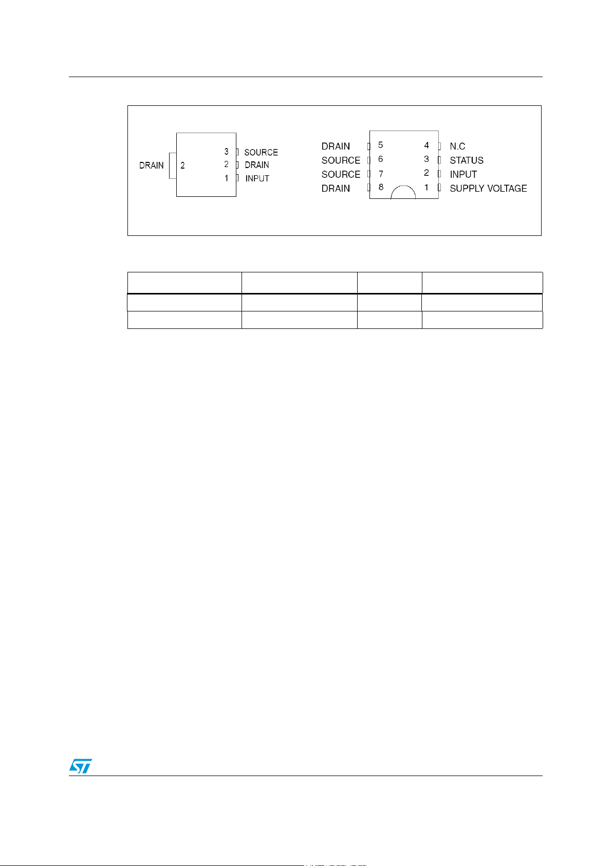
1 Block diagrams and pins configurations
Figure 1. VNL5050N3-E block diagram
Drain
Control & DiagnosticLOGIC
IN
DRIVER
(ACTIVE POWER LIMITATION)
Figure 2. VNL5050S5-E block diagram
SUPPLY
SUPPLY
LOGIC
Control & Diagnostic
OFF State
Open load
Current
Limitation
OVERTEMPERATURE
PROTECTION
OVERLOAD PROTECTION
Power
Clamp
GND
Drain
IN
ST
Current
Limitation
DRIVER
OVERTEMPERATURE
PROTECTION
OVERLOAD PROTECTION
(ACTIVE POWER LIMITATION)
Power
Clamp
GND
Doc ID 15917 Rev 4 5/32

Block diagrams and pins configurations VNL5050N3-E / VNL5050S5-E
Table 2. Pin function
Name Function
INPUT
Voltage controlled input pin with hysteresis, CMOS compatible. Controls output
switch state
(1)
DRAIN Power MOS drain
SOURCE Power MOS source and ground reference for the control section
SUPPLY
VOLTAGE
STATUS Open drain digital diagnostic pin
1. Internally connected to V
2. Valid for VNL5050S5-E only.
Supply voltage connected to the signal part (5 V)
(2)
in the VNL5050N3-E
supply
Figure 3. VNL5050N3-E current and voltage conventions
Figure 4. VNL5050S5-E current and voltage conventions
6/32 Doc ID 15917 Rev 4
VNL5050N3-E / VNL5050S5-E Block diagrams and pins configurations
Figure 5. Configuration diagrams (top view)
SOT-223
Table 3. Suggested connections for unused and n.c. pins
SO-8
Connection / pin STATUS N.C. INPUT
Floating X X X
To ground Not allowed X Through 10 kΩ resistor
Doc ID 15917 Rev 4 7/32
Absolute maximum rating VNL5050N3-E / VNL5050S5-E
2 Absolute maximum rating
Stressing the device above the rating listed in the Ta bl e 4 may cause permanent damage to
the device. These are stress ratings only and operation of the device at these or any other
conditions above those indicated in the operating sections of this specification is not implied.
Exposure to absolute maximum rating conditions for extended periods may affect device
reliability. Refer also to the STMicroelectronics SURE program and other relevant quality
document
2.1 Absolute maximum ratings
Table 4. Absolute maximum ratings
Val ue
Symbol Parameter
SOT-223 SO-8
Unit
V
- I
I
STAT
Drain-source voltage (V
DS
DC drain current Internally limited A
I
D
Reverse DC drain current -4 A
D
DC supply current - -1 to 10 mA
I
S
DC input current -1 to 10 mA
I
IN
DC status current - -1 to 10 mA
Electrostatic discharge
V
ESD1
(R = 1.5 kΩ; C = 100 pF)
– DRAIN
– SUPPLY, INPUT, STATUS
V
T
E
ESD2
Electrostatic discharge on output pin only
(R = 330 Ω, C = 150 pF)
Junction operating temperature -40 to 150 °C
T
j
Storage temperature -55 to 150 °C
stg
Single pulse avalanche energy
AS
(L = 1.1 mH, TJ= 150 °C, RL=0, I
2.2 Thermal data
= 0 V) Internally clamped V
IN
5000
4000
2000 V
OUT
= I
limL
)
93 mJ
V
Table 5. Thermal data
Symbol Parameter
R
thj-amb
1. When mounted on a standard single-sided FR4 board with 0.5 cm2 of Cu (at least 35 µm thick) connected
to all DRAIN pins
Thermal resistance junction-ambient 108.3
8/32 Doc ID 15917 Rev 4
Maximum value
SOT-223 SO-8
(1)
87 °C/W
Unit
VNL5050N3-E / VNL5050S5-E Electrical characteristics
3 Electrical characteristics
Values specified in this section are for V
supply
= V
= 4.5 V to 5.5 V, -40 °C < Tj < 150 °C,
IN
unless otherwise stated.
Table 6. Power MOS section
Symbol Parameter Test conditions Min. Typ. Max. Unit
V
R
V
CLAMP
V
I
Table 7. Source drain diode
Symbol Parameter Test conditions Min. Typ. Max. Unit
supply
ON
CLTH
DSS
Operating supply voltage - 3.5 5 5.5 V
I
= 2 A; Tj = 25 °C,
ON-state resistance
Drain-source clamp voltage V
Drain-source clamp
threshold voltage
D
= VIN = 5 V
V
supply
= 2 A; Tj = 150 °C,
I
D
V
= VIN = 5 V
supply
= 0 V; ID = 2 A 41 46 52 V
IN
= 0 V; ID = 2 mA 36 V
V
IN
V
= 0 V; V
IN
Tj = 25 °C
DS
= 13 V;
03
50
mΩ
100
OFF-state output current
V
= 0 V; V
IN
Tj = 125 °C
DS
= 13 V;
05
µA
V
Table 8. Input section
Forward on voltage ID = 2 A; V
SD
(1)
.
= 0 V - 0.8 - V
IN
Symbol Parameter Test conditions Min. Typ. Max. Unit
= V
I
Supply current from input pin
ISS
ON-state: V
= 0 V
V
DS
supply
= 5 V;
IN
30 110 µA
IS = 1 mA 5.5 7
V
V
1. Valid for VNL5050N3-E option (input and supply pins connected together)
Table 9. Status pin
Input clamp voltage
ICL
Input threshold voltage V
INTH
(1)
= -1 mA -0.7
I
S
= VIN; ID = 1 mA 1 3.5 V
DS
Symbol Parameter Test conditions Min. Typ. Max. Unit
V
STAT
I
LSTAT
C
STAT
Status low output voltage I
Status leakage current
Status pin input capacitance
= 1mA 0.5 V
STAT
Normal operation,
V
= 5 V
STAT
Normal operation,
V
= 5 V
STAT
10 µA
100 pF
V
Doc ID 15917 Rev 4 9/32

Electrical characteristics VNL5050N3-E / VNL5050S5-E
Table 9. Status pin
(1)
(continued)
Symbol Parameter Test conditions Min. Typ. Max. Unit
I
= 1 mA 5.5 7
V
1. Valid for VNL5050S5-E option
Table 10. Logic input
Status clamp voltage
STCL
(1)
STAT
= -1 mA -0.7
I
STAT
V
Symbol Parameter Test conditions Min. Typ. Max. Unit
V
Low-level input voltage - 0.9 V
IL
Low-level input current V
I
IL
V
High-level input voltage - 2.1 V
IH
High-level input current V
I
IH
I(hyst)
ICL
Input hysteresis voltage - 0.13 V
Input clamp voltage
V
V
1. Valid for VNL5050S5-E option
Table 11. Openload detection
(1)
= 0.9 V 1 µA
IN
= 2.1 V 10 µA
IN
= 1 mA 5.5 7
I
IN
= -1 mA -0.7
I
IN
V
Symbol Parameter Test conditions Min. Typ. Max. Unit
Openload OFF-state voltage
V
Ol
detection threshold
V
= 0 V 0.6 1.2 1.7 V
IN
Delay between INPUT falling
t
d(oloff)
edge and STATUS falling edge
I
= 0 A 45 425 1100 µs
OUT
in openload condition
1. Valid for VNL5050S5-E option
Table 12. Supply section
(1)
Symbol Parameter Test conditions Min. Typ. Max. Unit
I
Supply current
S
V
1. Valid for VNL5050S5-E option
Supply clamp voltage
SCL
OFF-state: T
= V
V
IN
ON-state: T
V
= 5 V; V
IN
I
= 1 mA 5.5 7
SCL
= -1 mA -0.7
I
SCL
DRAIN
= 25 °C;
j
= 0 V;
= 25 °C;
j
= 0 V
DS
10 25
µA
25 110
V
10/32 Doc ID 15917 Rev 4
 Loading...