

Quad high-side smart power solid-state relay
Features
Typ e V
VNI4140K VCC-41 V 0.08 Ω 0.7 A 41 V
1. Per channel.
■ Output current: 0.7 A per channel
■ Shorted load protections
■ Junction overtemperature protection
■ Case overtemperature protection for thermal
demag
(1)
R
independence of the channels
■ Thermal case shutdown restart not
simultaneous for the various channels
■ Protection against loss of ground
■ Current limitation
■ Undervoltage shutdown
■ Open drain diagnostic outputs
■ 3.3 V CMOS/TTL compatible inputs
■ Fast demagnetization of inductive loads
■ Conforms to IEC 61131-2
■ ESD according to IEC 61000-4-2 up to +/-
25 kV
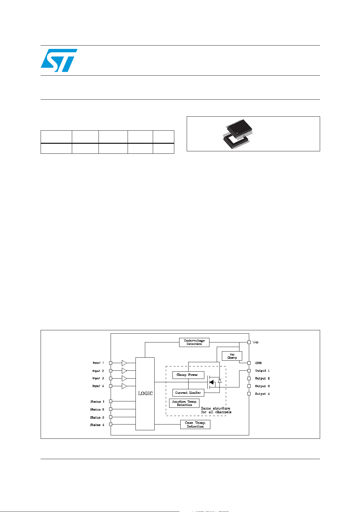
Figure 1. Block diagram
DS(on)
(1)
I
out
(1)
V
CC
VNI4140K
Datasheet − production data
PowerSSO-24
Description
The VNI4140K is a monolithic device made using
STMicroelectronics VIPower technology, intended
for driving four independent resistive or inductive
loads with one side connected to ground. Active
current limitation avoids dropping the system
power supply in case of shorted load. Built-in
thermal shutdown protects the chip from
overtemperature and short-circuit. In overload
condition, channel turns OFF and back ON
automatically so as to maintain junction
temperature between T
condition makes case temperature reach T
overloaded channel is turned OFF and will
restartonly when case temperature has
decreased down to T
channel in overload, re-start of the overloaded
channels will not be simultaneous, in order to
avoid high peak current from the supply. Non
overloaded channels continue to operate
normally. The open drain diagnostics outputs
indicates overtemperature conditions.
and TR. If this
TSD
. In case of more than one
CR
CSD
,
March 2012 Doc ID 14174 Rev 10 1/25
This is information on a product in full production.
www.st.com
25

Contents VNI1440K
Contents
1 Pin connection . . . . . . . . . . . . . . . . . . . . . . . . . . . . . . . . . . . . . . . . . . . . . . 3
2 Maximum ratings . . . . . . . . . . . . . . . . . . . . . . . . . . . . . . . . . . . . . . . . . . . . 5
2.1 Thermal data . . . . . . . . . . . . . . . . . . . . . . . . . . . . . . . . . . . . . . . . . . . . . . . 5
3 Electrical characteristics . . . . . . . . . . . . . . . . . . . . . . . . . . . . . . . . . . . . . 6
4 Truth table . . . . . . . . . . . . . . . . . . . . . . . . . . . . . . . . . . . . . . . . . . . . . . . . . 9
5 Typical application circuit . . . . . . . . . . . . . . . . . . . . . . . . . . . . . . . . . . . . 9
6 Switching waveforms . . . . . . . . . . . . . . . . . . . . . . . . . . . . . . . . . . . . . . . 11
7 Pin functions . . . . . . . . . . . . . . . . . . . . . . . . . . . . . . . . . . . . . . . . . . . . . . 12
8 Package and PC board thermal data . . . . . . . . . . . . . . . . . . . . . . . . . . . 14
8.1 VNI4140K thermal data . . . . . . . . . . . . . . . . . . . . . . . . . . . . . . . . . . . . . . 14
9 Reverse polarity protection . . . . . . . . . . . . . . . . . . . . . . . . . . . . . . . . . . 16
10 Package mechanical data . . . . . . . . . . . . . . . . . . . . . . . . . . . . . . . . . . . . 17
11 Order codes . . . . . . . . . . . . . . . . . . . . . . . . . . . . . . . . . . . . . . . . . . . . . . . 23
12 Revision history . . . . . . . . . . . . . . . . . . . . . . . . . . . . . . . . . . . . . . . . . . . 24
2/25 Doc ID 14174 Rev 10
VNI1440K Pin connection
1 Pin connection
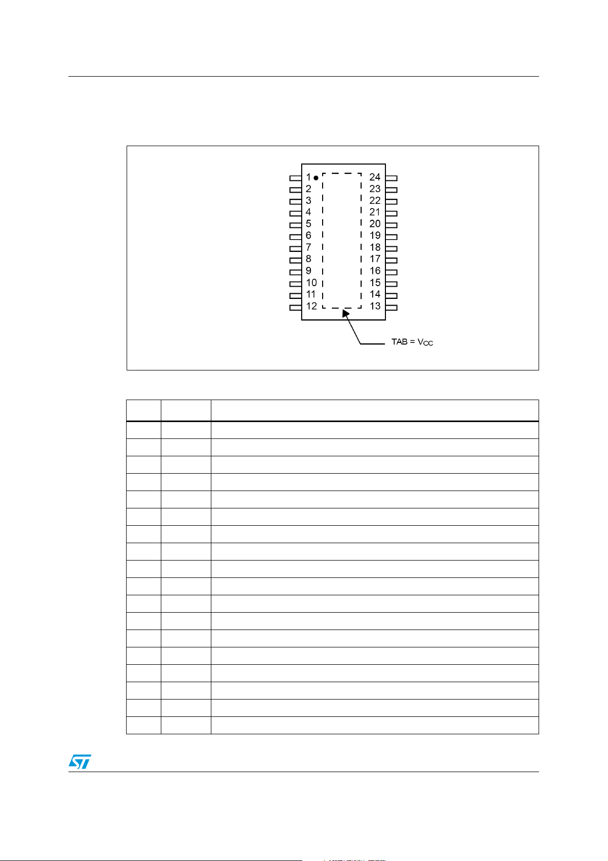
Figure 2. Pin connection (top view)
V
CC
IN1
STAT1
IN2
STAT2
GND
STAT3
IN3
STAT4
IN4
NC
NC
Table 1. Pin description
Pin Name Description
Tab TAB Exposed tab internally connected to Vcc
1 Vcc Supply voltage
2 IN1 Channel 1 input 3.3 V CMOS/TTL compatible
OUT1
OUT1
OUT1
OUT2
OUT2
OUT2
OUT3
OUT3
OUT3
OUT4
OUT4
OUT4
3 STAT1 Channel 1 status in open drain configuration
4 IN2 Channel 2 input 3.3 V CMOS/TTL compatible
5 STA2 Channel 2 status in open drain configuration
6 GND Device ground connection
7 STAT3 Channel 3 status in open drain configuration
8 IN3 Channel 3 input 3.3 V CMOS/TTL compatible
9 STAT4 Channel 4 status in open drain configuration
10 IN4 Channel 4 input 3.3 V CMOS/TTL compatible
11 NC
12 NC
13 OUT4 Channel 4 power stage output, internally protected
14 OUT4 Channel 4 power stage output, internally protected
15 OUT4 Channel 4 power stage output, internally protected
16 OUT3 Channel 3 power stage output, internally protected
17 OUT3 Channel 3 power stage output, internally protected
Doc ID 14174 Rev 10 3/25

Pin connection VNI1440K
Table 1. Pin description (continued)
Pin Name Description
18 OUT3 Channel 3 power stage output, internally protected
19 OUT2 Channel 2 power stage output, internally protected
20 OUT2 Channel 2 power stage output, internally protected
21 OUT2 Channel 2 power stage output, internally protected
22 OUT1 Channel 1 power stage output, internally protected
23 OUT1 Channel 1 power stage output, internally protected
24 OUT1 Channel 1 power stage output, internally protected
4/25 Doc ID 14174 Rev 10
VNI1440K Maximum ratings
2 Maximum ratings
Table 2. Absolute maximum rating
Symbol Parameter Value Unit
V
-V
I
I
V
I
V
E
P
T
GND
OUT
V
STAT
Power supply voltage 41 V
CC
Reverse supply voltage -0.3 V
CC
DC ground reverse current -250 mA
Output current (continuos) Internally limited A
I
Reverse output current (per channel) -5 A
R
I
Input current (per channel) ± 10 mA
IN
Input voltage +V
IN
Status pin voltage +V
STAT
Status pin current ± 10 mA
Electrostatic discharge (R = 1.5 kΩ; C = 100 pF) 2000 V
ESD
Single pulse avalanche energy per channel not
AS
simultaneously
Power dissipation at Tc = 25 °C Internally limited W
TOT
T
Junction operating temperature Internally limited °C
J
Storage temperature -55 to 150 °C
STG
2.1 Thermal data
CC
CC
V
V
300 mJ
Table 3. Thermal data
Symbol Parameter Value Unit
R
th(JC)
R
th(JA)
1. Per channel
Thermal resistance junction-case
Thermal resistance junction-ambient Max see Figure 11 °C/W
Doc ID 14174 Rev 10 5/25
(1)
Max 2 °C/W
Electrical characteristics VNI1440K
3 Electrical characteristics
10.5 V < VCC < 36 V; -25 °C < TJ < 125 °C; unless otherwise specified
Table 4. Power section
Symbol Parameter Test condition Min Typ Max Unit
Vcc Supply voltage 10.5 36 V
I
R
DS(on)
V
clamp
I
S
I
LGND
V
OUT(OFF)
On-state resistance
Supply current
Output current at turnoff
Off state output
voltage
= 0.5 A at TJ = 25 °C
OUT
I
= 0.5 A
OUT
Is = 20 mA 41 45 52 V
All channel in OFF state
ON state with V
= 125 °C)
(T
J
VCC = V
V
V
STAT
= 24 V, V
GND
= 0 V and I
IN
= 5 V
IN
= VIN =
= 0 V
OUT
= 0 A 1 V
OUT
250
2.4 4
0.080
0.140ΩΩ
µA
mA
1mA
CP
Off state output
current
Charge pump
frequency
V
IN
= V
= 0 V 0 5 µA
OUT
Channel in ON state
(1)
1450 kHz
I
OUT(OFF)
F
1. To cover EN55022 class A and class B normative.
= 24 V; -25 °C < TJ < 125 °C, RL = 48 Ω, input rise time < 0.1 µs
V
CC
Table 5. Switching
Symbol Parameter Min Typ Max Unit
t
d
t
d
(OFF)
dV/dt
dV/dt
(ON)
Turn on delay - 20 - µs
t
Rise time - 10 - µs
r
Turn off - 30 - µs
t
Fall time - 8 - µs
f
Turn on voltage slope - 3 - V/µs
(ON)
(off) Turn off voltage slope - 4 - V/µs
6/25 Doc ID 14174 Rev 10
VNI1440K Electrical characteristics
Table 6. Logical input
Symbol Parameter Test condition Min Typ Max Unit
V
V
V
I(HYST)
I
Input low level voltage 0.8 V
IL
Input high level voltage 2.20 V
IH
Input hysteresis
voltage
Input current
IN
V
= 15 V 10
IN
= 36 V 210
V
IN
0.15 V
Table 7. Protection and diagnostic
Symbol Parameter Test condition Min Typ Max Unit
v
STAT
V
USD
V
USDHYS
I
LIM
I
PEAK
Status voltage
output low
Undervoltage
protection
Undervoltage
hysteresis
DC short-circuit
current
Maximum DC output
current
= 1.6 mA 0.6 V
I
STAT
710.5V
0.4 0.5 V
V
CC
= 24 V; R
< 10 mΩ 0.7 1 1.7 A
LOAD
Dynamic load 1.3 A
µΑ
Hyst Tracking limits 0.2 A
I
LSTAT
T
T
T
HIST
T
CSD
T
T
CHYST
V
demag
TSD
Status leakage current VCC = V
Junction shutdown
temperature
Junction reset
R
temperature
Junction thermal
hysteresis
Case shutdown
temperature
Case reset
CR
temperature
Case thermal
hysteresis
Output voltage at
turn-OFF
I
OUT
= 36 V 30 µΑ
STAT
= 0.5 A; L
LOAD
>= 1 mH
150 170 190 °C
135 °C
715 °C
125 130 135 °C
110 °C
715 °C
-41VCC-45VCC-
V
CC
52
V
Doc ID 14174 Rev 10 7/25
Electrical characteristics VNI1440K
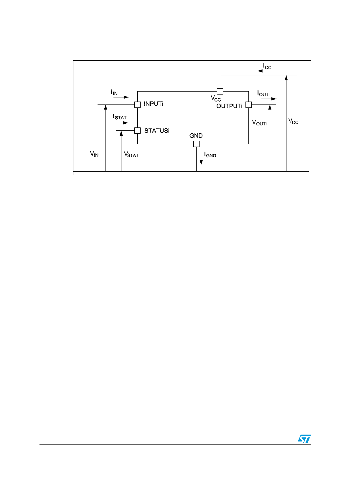
Figure 3. Current and voltage conventions
8/25 Doc ID 14174 Rev 10
 Loading...