

Features
Typ e R
VNH5019A-E
■ ECOPACK
■ Automotive Grade: compliance with AEC
DS(on)
18 mΩ typ
(per leg)
®
: lead free and RoHS compliant
I
out
30 A 41 V
guidelines
■ Output current: 30 A
■ 3 V CMOS compatible inputs
■ Undervoltage and overvoltage shutdown
■ High-side and low-side thermal shutdown
■ Cross-conduction protection
■ Current limitation
■ Very low standby power consumption
■ PWM operation up to 20 khz
■ Protection against:
– Loss of ground and loss of V
■ Current sense output proportional to motor
CC
current
■ Charge pump output for reverse polarity
protection
■ Output protected against short to ground and
short to V
CC
Description
The VHN5019A-E is a full bridge motor driver
intended for a wide range of automotive
applications. The device incorporates a dual
monolithic high-side drivers and two low-side
switches. The high-side driver switch is designed
using STMicroelectronics’ well known and proven
proprietary VIPower
to efficiently integrate on the same die a true
®
M0 technology that allows
VNH5019A-E
Automotive fully integrated
H-bridge motor driver
V
ccmax
MultiPowerSO-30™
Power MOSFET with an intelligent
signal/protection circuit.
The three dice are assembled in
MultiPowerSO-30 package on electrically isolated
lead-frames. This package, specifically designed
for the harsh automotive environment offers
improved thermal performance thanks to exposed
die pads. The input signals IN
directly interface to the microcontroller to select
the motor direction and the brake condition.
The DIAG
/ENA or DIAGB/ENB, when connected
A
to an external pull-up resistor, enable one leg of
the bridge. They also provide a feedback digital
diagnostic signal. The CS pin allows to monitor
the motor current by delivering a current
proportional to its value when CS_DIS pin is
driven low or left open. The PWM, up to 20 KHz,
lets us to control the speed of the motor in all
possible conditions. In all cases, a low-level state
on the PWM pin turns-off both the LS
switches. When PWM rises to a high-level, LS
LS
turn-on again depending on the input pin
B
state.
Output current limitation and thermal shutdown
protects the concerned high-side in short to
ground condition.
The short to battery condition is revealed by the
overload detector or by thermal shutdown that
latches off the relevant low-side.
Active V
pin voltage clamp protects the device
CC
against low energy spikes in all configurations for
the motor.
CP pin provides the necessary gate drive for an
external n-channel PowerMOS used for reverse
polarity protection.
and INB can
A
and LSB
A
A
or
December 2011 Doc ID 15701 Rev 8 1/37
www.st.com
1

Contents VNH5019A-E
Contents
1 Block diagram and pin description . . . . . . . . . . . . . . . . . . . . . . . . . . . . . 5
2 Electrical specifications . . . . . . . . . . . . . . . . . . . . . . . . . . . . . . . . . . . . . . 9
2.1 Absolute maximum ratings . . . . . . . . . . . . . . . . . . . . . . . . . . . . . . . . . . . . . 9
2.2 Thermal data . . . . . . . . . . . . . . . . . . . . . . . . . . . . . . . . . . . . . . . . . . . . . . 10
2.3 Electrical characteristics . . . . . . . . . . . . . . . . . . . . . . . . . . . . . . . . . . . . . . 11
2.4 Waveforms and truth table . . . . . . . . . . . . . . . . . . . . . . . . . . . . . . . . . . . . 14
2.5 Reverse battery protection . . . . . . . . . . . . . . . . . . . . . . . . . . . . . . . . . . . . 19
3 Package and PCB thermal data . . . . . . . . . . . . . . . . . . . . . . . . . . . . . . . 26
3.1 MultiPowerSO-30 thermal data . . . . . . . . . . . . . . . . . . . . . . . . . . . . . . . . 26
3.1.1 Thermal calculation in clockwise and anti-clockwise operation in
steady-state mode . . . . . . . . . . . . . . . . . . . . . . . . . . . . . . . . . . . . . . . . . 27
3.1.2 Thermal calculation in transient mode . . . . . . . . . . . . . . . . . . . . . . . . . . 27
4 Package and packing information . . . . . . . . . . . . . . . . . . . . . . . . . . . . . 30
4.1 ECOPACK® . . . . . . . . . . . . . . . . . . . . . . . . . . . . . . . . . . . . . . . . . . . . . . . 30
4.2 MultiPowerSO-30 mechanical data . . . . . . . . . . . . . . . . . . . . . . . . . . . . . 30
4.3 MultiPowerSO-30 suggested land pattern . . . . . . . . . . . . . . . . . . . . . . . . 32
4.4 MultiPowerSO-30 packing information . . . . . . . . . . . . . . . . . . . . . . . . . . . 33
5 Order codes . . . . . . . . . . . . . . . . . . . . . . . . . . . . . . . . . . . . . . . . . . . . . . . 34
6 Revision history . . . . . . . . . . . . . . . . . . . . . . . . . . . . . . . . . . . . . . . . . . . 35
2/37 Doc ID 15701 Rev 8

VNH5019A-E List of tables
List of tables
Table 1. Suggested connections for unused and not connected pins . . . . . . . . . . . . . . . . . . . . . . . . 6
Table 2. Pin definitions and functions . . . . . . . . . . . . . . . . . . . . . . . . . . . . . . . . . . . . . . . . . . . . . . . . . 6
Table 3. Block descriptions . . . . . . . . . . . . . . . . . . . . . . . . . . . . . . . . . . . . . . . . . . . . . . . . . . . . . . . . . 7
Table 4. Absolute maximum rating . . . . . . . . . . . . . . . . . . . . . . . . . . . . . . . . . . . . . . . . . . . . . . . . . . . 9
Table 5. Thermal data. . . . . . . . . . . . . . . . . . . . . . . . . . . . . . . . . . . . . . . . . . . . . . . . . . . . . . . . . . . . 10
Table 6. Power section . . . . . . . . . . . . . . . . . . . . . . . . . . . . . . . . . . . . . . . . . . . . . . . . . . . . . . . . . . . 11
Table 7. Logic inputs (INA, INB, ENA, ENB,PWM, CS_DIS) . . . . . . . . . . . . . . . . . . . . . . . . . . . . . . 11
Table 8. Switching (V
Table 9. Protection and diagnostic . . . . . . . . . . . . . . . . . . . . . . . . . . . . . . . . . . . . . . . . . . . . . . . . . . 12
Table 10. Current sense (8 V < V
Table 11. Charge pump . . . . . . . . . . . . . . . . . . . . . . . . . . . . . . . . . . . . . . . . . . . . . . . . . . . . . . . . . . . 14
Table 12. Truth table in normal operating conditions . . . . . . . . . . . . . . . . . . . . . . . . . . . . . . . . . . . . . 14
Table 13. Truth table in fault conditions (detected on OUTA). . . . . . . . . . . . . . . . . . . . . . . . . . . . . . . 16
Table 14. Electrical transient requirements (part 1) . . . . . . . . . . . . . . . . . . . . . . . . . . . . . . . . . . . . . . 18
Table 15. Electrical transient requirements (part 2) . . . . . . . . . . . . . . . . . . . . . . . . . . . . . . . . . . . . . . 18
Table 16. Electrical transient requirements (part 3) . . . . . . . . . . . . . . . . . . . . . . . . . . . . . . . . . . . . . . 18
Table 17. Thermal calculation in clockwise and anti-clockwise operation in steady-state mode . . . . 27
Table 18. Thermal parameters . . . . . . . . . . . . . . . . . . . . . . . . . . . . . . . . . . . . . . . . . . . . . . . . . . . . . . 29
Table 19. MultiPowerSO-30 mechanical data . . . . . . . . . . . . . . . . . . . . . . . . . . . . . . . . . . . . . . . . . . 31
Table 20. Device summary . . . . . . . . . . . . . . . . . . . . . . . . . . . . . . . . . . . . . . . . . . . . . . . . . . . . . . . . . 34
Table 21. Document revision history . . . . . . . . . . . . . . . . . . . . . . . . . . . . . . . . . . . . . . . . . . . . . . . . . 35
= 13 V, R
CC
= 0.87 W, Tj = 25 °C) . . . . . . . . . . . . . . . . . . . . . . . . . . . . . 12
LOAD
< 21 V). . . . . . . . . . . . . . . . . . . . . . . . . . . . . . . . . . . . . . . . . . . . 13
CC
Doc ID 15701 Rev 8 3/37

List of figures VNH5019A-E
List of figures
Figure 1. Block diagram . . . . . . . . . . . . . . . . . . . . . . . . . . . . . . . . . . . . . . . . . . . . . . . . . . . . . . . . . . . . 5
Figure 2. Configuration diagram (top view) . . . . . . . . . . . . . . . . . . . . . . . . . . . . . . . . . . . . . . . . . . . . . 6
Figure 3. Current and voltage conventions . . . . . . . . . . . . . . . . . . . . . . . . . . . . . . . . . . . . . . . . . . . . . 9
Figure 4. Typical application circuit for DC to 20 kHz PWM operation with reverse battery protection
(option A) . . . . . . . . . . . . . . . . . . . . . . . . . . . . . . . . . . . . . . . . . . . . . . . . . . . . . . . . . . . . . . 15
Figure 5. Typical application circuit for DC to 20 kHz PWM operation with reverse battery protection
(option B) . . . . . . . . . . . . . . . . . . . . . . . . . . . . . . . . . . . . . . . . . . . . . . . . . . . . . . . . . . . . . . 16
Figure 6. Behavior in fault condition (how a fault can be cleared) . . . . . . . . . . . . . . . . . . . . . . . . . . . 17
Figure 7. Definition of the delay times measurement . . . . . . . . . . . . . . . . . . . . . . . . . . . . . . . . . . . . 19
Figure 8. Definition of the low-side switching times . . . . . . . . . . . . . . . . . . . . . . . . . . . . . . . . . . . . . . 20
Figure 9. Definition of the high-side switching times . . . . . . . . . . . . . . . . . . . . . . . . . . . . . . . . . . . . . 20
Figure 10. Definition of dynamic cross conduction current during a PWM operation. . . . . . . . . . . . . . 21
Figure 11. Waveforms in full bridge operation (part 1). . . . . . . . . . . . . . . . . . . . . . . . . . . . . . . . . . . . . 22
Figure 12. Waveforms in full bridge operation (part 2). . . . . . . . . . . . . . . . . . . . . . . . . . . . . . . . . . . . . 23
Figure 13. Definition of delay response time of sense current . . . . . . . . . . . . . . . . . . . . . . . . . . . . . . . 24
Figure 14. Half-bridge configuration. . . . . . . . . . . . . . . . . . . . . . . . . . . . . . . . . . . . . . . . . . . . . . . . . . . 24
Figure 15. Multi-motors configuration . . . . . . . . . . . . . . . . . . . . . . . . . . . . . . . . . . . . . . . . . . . . . . . . . 25
Figure 16. MultiPowerSO-30™ PC board . . . . . . . . . . . . . . . . . . . . . . . . . . . . . . . . . . . . . . . . . . . . . . 26
Figure 17. Chipset configuration . . . . . . . . . . . . . . . . . . . . . . . . . . . . . . . . . . . . . . . . . . . . . . . . . . . . . 26
Figure 18. Auto and mutual Rthj-amb vs PCB copper area in open box free air condition . . . . . . . . . 26
Figure 19. Chipset configuration . . . . . . . . . . . . . . . . . . . . . . . . . . . . . . . . . . . . . . . . . . . . . . . . . . . . . 27
Figure 20. MultiPowerSO-30 HSD thermal impedance junction ambient single pulse . . . . . . . . . . . . 28
Figure 21. MultiPowerSO-30 LSD thermal impedance junction ambient single pulse . . . . . . . . . . . . . 28
Figure 22. Thermal fitting model of an H-bridge in MultiPowerSO-30 . . . . . . . . . . . . . . . . . . . . . . . . . 29
Figure 23. MultiPowerSO-30 package dimensions . . . . . . . . . . . . . . . . . . . . . . . . . . . . . . . . . . . . . . . 30
Figure 24. MultiPowerSO-30 suggested pad layout . . . . . . . . . . . . . . . . . . . . . . . . . . . . . . . . . . . . . . 32
Figure 25. MultiPowerSO-30 tube shipment (no suffix) . . . . . . . . . . . . . . . . . . . . . . . . . . . . . . . . . . . 33
Figure 26. MultiPowerSO-30 tape and reel shipment (suffix “TR”) . . . . . . . . . . . . . . . . . . . . . . . . . . . 33
4/37 Doc ID 15701 Rev 8
VNH5019A-E Block diagram and pin description
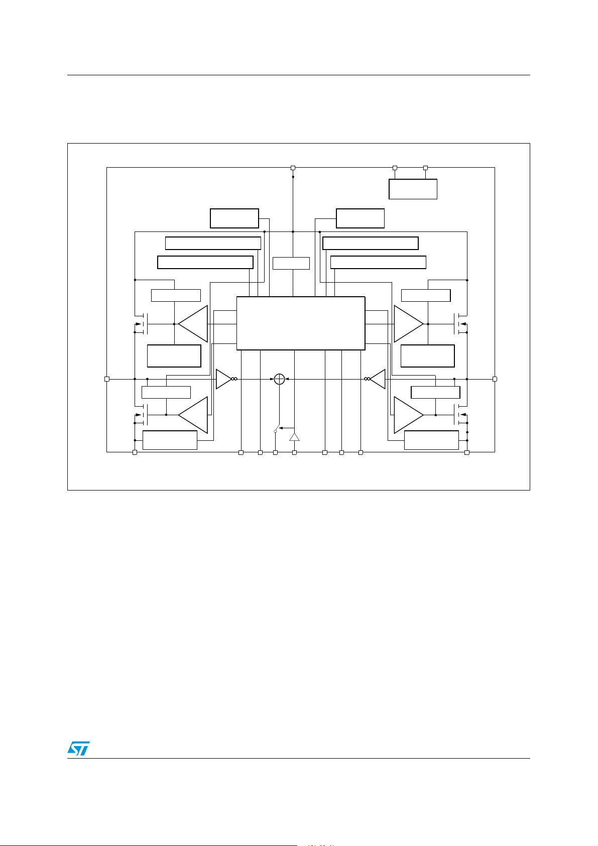
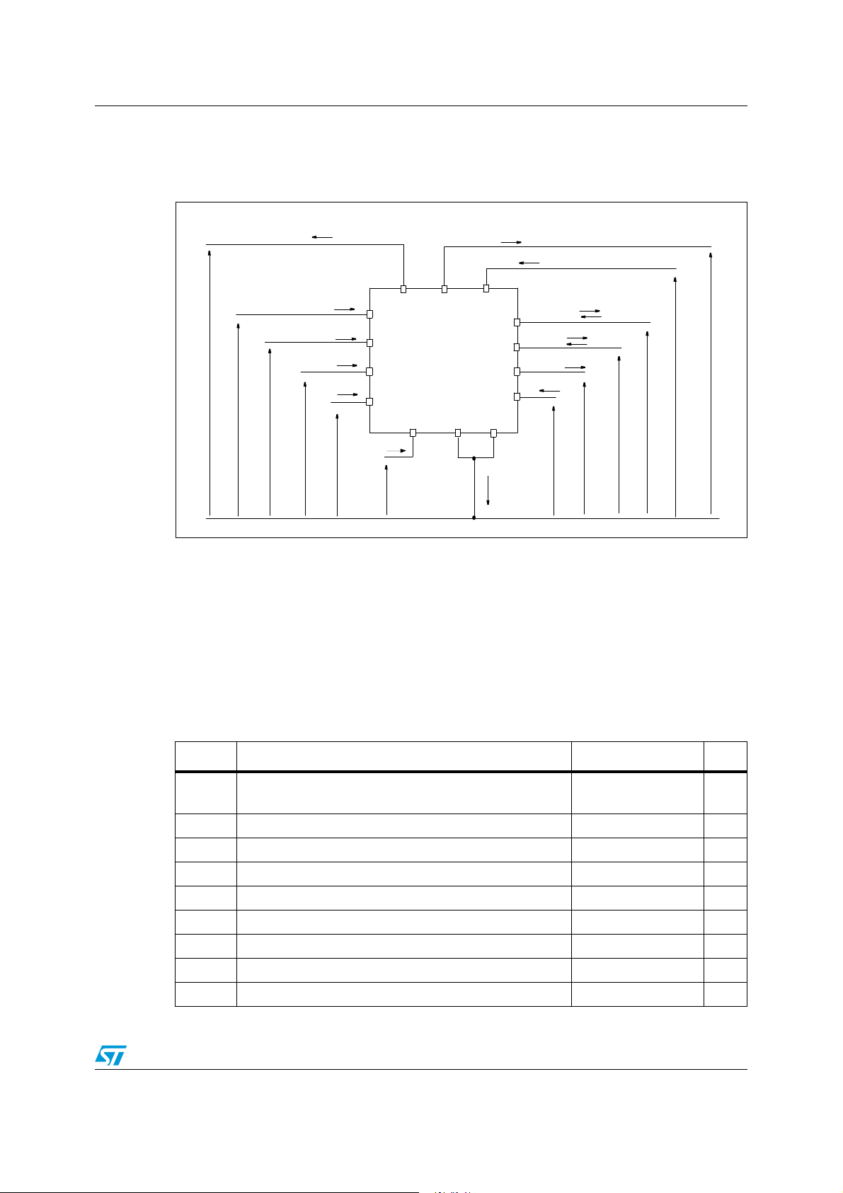
1 Block diagram and pin description
Figure 1. Block diagram
6
##
#(!2'%
05-
0
/54
&!5,4
$%4%#4)/.
,3!?/6%24%-0%2!452%
/65
6
#,!-0?(3
(3
!
#522%.4
,)-)4!4 )/.?!
!
#,!-0?,3
,3
!
/6%2,/!$
$%4%#4/2?!
'.$
!
$2)6%2
!
$2)6%2
!
(3
!
+
,3
!
,/')#
$)!'!%.!).!#3 #3?$)3 07- )."$)!'"%.
0/7%2
,)-)4! 4)/.
,3"?/6%24%-0%2!4 52%
(3"?/6%24%-0%2!452%(3!?/6%24%-0%2!452%
$2)6%2
(3
#522%.4
,)-)4!4 )/.?"
+
$2)6%2
,3
"
#,!-0?(3
"
#,!-0?,3
"
/6%2,/!$
$%4%#4
"
/2?"
(3
"
/54
"
"
,3
"
'.$
"
("1($'5
Doc ID 15701 Rev 8 5/37
Block diagram and pin description VNH5019A-E
Figure 2. Configuration diagram (top view)
OUT
N.C.
V
IN
ENA/DIAG
CC
A
A
A
1
OUT
A
Heat Slug2
30
CS_DIS
EN
/DIAG
B
PWM
CS
IN
B
B
V
CC
Heat Slug1
CP
V
BAT
V
CC
OUT
B
Heat Slug3
N.C.
OUT
B
Table 1. Suggested connections for unused and not connected pins
15 16
Connection / pin Current sense N.C. OUTx
OUT
A
N.C.
GND
A
GND
A
GND
A
OUT
A
N.C.
V
CC
N.C.
OUT
B
GND
B
GND
B
GND
B
N.C.
OUT
B
INPUTx, PWM
DIAGx/ENx
CS_DIS
Floating Not allowed X X X
To ground Through 1 kΩ resistor X Not allowed
Table 2. Pin definitions and functions
Through 10 kΩ
resistor
Pin Symbol Function
1, 25, 30
2,14,17, 22,
24,29
3, 13, 23
12 V
OUTA,
Heat Slug2
N.C. Not connected
,
V
CC
Heat Slug1
BAT
Source of high-side switch A / drain of low-side switch A, power
connection to the motor
Drain of high-side switches and connection to the drain of the
external PowerMOS used for the reverse battery protection
Battery connection and connection to the source of the external
PowerMOS used for the reverse battery protection
Status of high-side and low-side switches A; open drain output.
This pin must be connected to an external pull-up resistor. When
externally pulled low, it disables half-bridge A. In case of fault
5EN
/DIAG
A
detection (thermal shutdown of a high-side FET or excessive
A
ON-state voltage drop across a low-side FET), this pin is pulled
low by the device (see
(detected on OUTA)
Table 13: Truth table in fault conditions
)
6/37 Doc ID 15701 Rev 8
VNH5019A-E Block diagram and pin description
Table 2. Pin definitions and functions (continued)
Pin Symbol Function
6CS_DIS
4IN
A
Active high CMOS compatible pin to disable the current sense
pin
Clockwise input. CMOS compatible
7 PWM PWM input. CMOS compatible.
Output of current sense. This output delivers a current
8CS
proportional to the motor current, if CS_DIS is low or left open.
The information can be read back as an analog voltage across
an external resistor.
Status of high-side and low-side switches B; Open drain output.
This pin must be connected to an external pull up resistor. When
externally pulled low, it disables half-bridge B. In case of fault
9EN
/DIAG
B
detection (thermal shutdown of a high-side FET or excessive
B
ON-state voltage drop across a low-side FET), this pin is pulled
low by the device (see
(detected on OUTA)
10 IN
B
11 CP
OUT
15, 16, 21
26, 27, 28 GND
18, 19, 20 GND
1. GNDA and GNDB must be externally connected together
B,
Heat Slug3
A
B
Counter clockwise input. CMOS compatible
Connection to the gate of the external MOS used for the reverse
battery protection
Source of high-side switch B / drain of low-side switch B, power
connection to the motor
Source of low-side switch A and power ground
Source of low-side switch B and power ground
Table 13: Truth table in fault conditions
.
(1)
(1)
)
Table 3. Block descriptions
(1)
Name Description
Logic control
Overvoltage + undervoltage
High-side, low-side and clamp
voltage
High-side and low-side driver
Linear current limiter
High-side and low-side
overtemperature protection
Low-side overload detector
Allows the turn-on and the turn-off of the high-side and the
low-side switches according to the
Ta bl e 12
.
Shut down the device outside the range [4.5 V to 24 V] for the
battery voltage.
Protect the high-side and the low-side switches from the
high-voltage on the battery line in all configuration for the motor.
Drive the gate of the concerned switch to allow a proper R
DS(on)
for the leg of the bridge.
Limits the motor current, by reducing the high-side switch
gate-source voltage when short-circuit to ground occurs.
In case of short-circuit with the increase of the junction’s
temperature, it shuts down the concerned driver to prevent its
degradation and to protect the die.
Detects when low-side current exceeds shutdown current and
latches off the concerned low-side.
Doc ID 15701 Rev 8 7/37

Block diagram and pin description VNH5019A-E
Table 3. Block descriptions
Name Description
Charge pump
Fault detection
Power limitation
1. See
Figure 1
(1)
(continued)
Provides the voltage necessary to drive the gate of the external
PowerMOS used for the reverse polarity protection
Signalizes an abnormal condition of the switch (output
shorted to ground or output shorted to battery) by pulling
down the concerned ENx/DIAGx pin.
Limits the power dissipation of the high-side driver inside
safe range in case of short to ground condition.
8/37 Doc ID 15701 Rev 8
VNH5019A-E Electrical specifications
2 Electrical specifications
Figure 3. Current and voltage conventions
I
CP
V
CP
I
INA
I
V
INA
V
INB
INB
I
ENA
IN
IN
CP
A
B
DIAGA/EN
I
ENB
V
ENA
V
ENB
DIAGB/EN
PWM
I
pw
V
pw
2.1 Absolute maximum ratings
Stressing the device above the rating listed in the “absolute maximum ratings” table may
cause permanent damage to the device. These are stress ratings only and operation of the
device at these or any other conditions above those indicated in the operating sections of
this specification is not implied. Exposure to absolute maximum rating conditions for
extended periods may affect device reliability. Refer also to the STMicroelectronics SURE
program and other relevant quality document.
Table 4. Absolute maximum rating
I
BAT
I
S
BAT
GND
V
CC
CS_DIS
GND
A
OUT
OUT
CS
I
A
B
I
SENSE
I
CSD
V
B
CSD
I
OUTB
V
SENSE
OUTA
V
OUTB
V
OUTA
V
A
B
V
BAT
V
CC
GND
I
GND
Symbol Parameter Value Unit
V
V
I
max
I
I
I
I
CS_DIS
Maximum battery voltage
BAT
Maximum bridge supply voltage + 41 V
CC
Maximum output current (continuous) 30 A
I
Reverse output current (continuous) -30 A
R
I
Input current (INA and INB pins) +/- 10 mA
IN
Enable input current (DIAGA/ENA and DIAGB/ENB pins) +/- 10 mA
EN
PWM input current +/- 10 mA
pw
CP output current +/- 10 mA
CP
CS_DIS input current +/- 10 mA
(1)
-16
+41
V
V
Doc ID 15701 Rev 8 9/37
Electrical specifications VNH5019A-E
Table 4. Absolute maximum rating (continued)
Symbol Parameter Value Unit
V
- 41
V
V
T
1. This applies with the n-channel MOSFET used for the reverse battery protection. Otherwise V
shorted to VCC.
Current sense maximum voltage
CS
Electrostatic discharge (human body model: R = 1.5 kΩ,
ESD
C = 100 pF)
Case operating temperature -40 to 150 °C
T
c
Storage temperature -55 to 150 °C
STG
CC
+V
CC
2kV
has to be
BAT
V
V
2.2 Thermal data
Table 5. Thermal data
Symbol Parameter Max. value Unit
R
thj-case
R
thj-amb
Thermal resistance junction-case HSD 1.7 °C/W
Thermal resistance junction-case LSD 3.2 °C/W
Thermal resistance junction-ambient See
Figure 18
°C/W
10/37 Doc ID 15701 Rev 8
VNH5019A-E Electrical specifications
2.3 Electrical characteristics
Values specified in this section are for 8 V < V
< 21 V, -40 °C < Tj < 150 °C, unless
CC
otherwise specified.
Table 6. Power section
Symbol Parameter Test conditions Min. Typ. Max. Unit
V
CC
I
S
R
ONHS
R
ONLS
V
f
I
L(off)
Operating bridge supply
voltage
Supply current
Static high-side
resistance
Static low-side
resistance
High-side
free-wheeling diode
forward voltage
High-side OFF-state
output current (per
channel)
5.5 24 V
OFF-state with all fault cleared and ENx = 0 V
(standby):
= INB = PWM = 0; Tj = 25 °C; VCC = 13 V
IN
A
IN
= INB = PWM = 0
A
10 15
OFF-state (no standby):
INA = INB = PWM = 0; ENx = 5 V
ON-state:
IN
or INB = 5 V, no PWM
A
488mA
INA or INB = 5 V, PWM = 20 kHz
I
= 15 A; Tj = 25 °C 12.0
OUT
I
= 15 A; Tj = - 40 °C to 150 °C 26.5
OUT
= 15 A; Tj = 25 °C 6.0
I
OUT
= 15 A; Tj = - 40 °C to 150 °C 11.5
I
OUT
= 15 A,
I
f
= 150 °C
T
j
= 25 °C; V
T
j
= 125 °C; V
T
j
= ENX = 0 V; VCC = 13 V 3
OUTX
= ENX = 0 V; VCC = 13 V 5
OUTX
0.6 0.8 V
60
6
µA
µA
mA
mA
mΩ
mΩ
µA
Table 7. Logic inputs (INA, INB, ENA, ENB,PWM, CS_DIS)
Symbol Parameter Test conditions Min. Typ. Max. Unit
V
Low-level input voltage
IL
High-level input
V
IH
voltage
I
Low-level input current V
INL
High-level input
I
INH
current
IHYST
Input hysteresis
voltage
V
Normal operation (DIAG
acts as an input pin)
Normal operation (DIAGX/ENX pin
acts as an input pin)
= 0.9 V 1 µA
IN
V
= 2.1 V 10 µA
IN
Normal operation (DIAGX/ENX pin
acts as an input pin)
/ENX pin
X
0.9 V
2.1 V
0.15 V
Doc ID 15701 Rev 8 11/37
Electrical specifications VNH5019A-E
Table 7. Logic inputs (INA, INB, ENA, ENB,PWM, CS_DIS) (continued)
Symbol Parameter Test conditions Min. Typ. Max. Unit
I
= 1 mA 5.5 6.3 7.5
V
V
Table 8. Switching (VCC = 13 V, R
Input clamp voltage
ICL
Enable low-level
DIAG
output voltage
Symbol Parameter Test conditions Min Typ Max Unit
f PWM frequency 0 20 kHz
t
d(on)
HSD rise time
IN
= -1 mA -1.0 -0.7 -0.3
I
IN
Fault operation (DIAGX/ENX pin
acts as an output pin); I
= 0.87 Ω, Tj = 25 °C)
LOAD
= 1 mA
EN
Input rise time < 1µs
(see
Figure 9
)
V
0.4 V
250 µs
t
d(off)
t
t
t
DEL
t
rr
I
RM
Table 9. Protection and diagnostic
HSD fall time
LSD rise time (see
r
LSD fall time (see
f
Delay time during change of
operating mode
High-side free wheeling
diode reverse recovery time
Dynamic cross-conduction
current
Input rise time < 1µs
(see
(see
(see
I
OUT
(see
Figure 9
Figure 8
Figure 8
Figure 7
Figure 10
= 15 A
Figure 10
)
)12µs
)12µs
) 200 400 1600 µs
)110ns
)
250 µs
2A
Symbol Parameter Test conditions Min Typ Max Unit
V
USD
V
USDhyst
V
OV
I
LIM_H
I
SD_LS
VCC undervoltage
shutdown
V
undervoltage
CC
shutdown hysteresis
V
overvoltage shutdown 24 27 30 V
CC
4.5 5.5 V
0.5 V
High-side current limitation 30 50 70 A
Low-side shutdown current 70 115 160 A
High-side clamp voltage
V
CLPHS
(1)
(VCC to OUTA = 0 or
= 0)
OUT
B
= 15 A 43 48 54 V
I
OUT
Low-side clamp voltage
(1)
V
CLPLS
T
TSD
(OUTA = V
OUT
B
Thermal shutdown
(2)
temperature
or
CC
= VCC to GND)
= 15 A 27 30 33 V
I
OUT
= 2.1 V 150 175 200 °C
V
IN
12/37 Doc ID 15701 Rev 8
 Loading...