

Features
VNH3ASP30-E
Automotive fully integrated H-bridge motor driver
Type R
VNH3ASP30-E
■ 5V logic level compatible inputs
■ Undervoltage and overvoltage shutdown
■ Overvoltage clamp
■ Thermal shut down
■ Cross-conduction protection
■ Linear current limiter
■ Very low standby power consumption
■ PWM operation up to 20 kHz
■ Protection against loss of ground and loss of
V
CC
■ Current-sense output proportional to motor
DS(on)
42mΩ max
(per leg)
I
V
out
30A 41V
ccmax
current
■ Package: ECOPACK
®
Description
The VNH3ASP30-E is a full-bridge motor driver
intended for a wide range of automotive
applications. The device incorporates a dual
monolithic high-side driver (HSD) and two lowside switches. The HSD switch is designed using
STMicroelectronics proprietary VIPower™ M0
technology that efficiently integrates a true Power
MOSFET with an intelligent signal/protection
circuit on the same die.
MultiPowerSO-30™
The low-side switches are vertical MOSFETs
manufactured using STMicroelectronics
proprietary EHD (“STripFET™”) process.The
three circuits are assembled in a MultiPowerSO30 package on electrically isolated lead frames.
This package, specifically designed for the harsh
automotive environment, offers improved thermal
performance thanks to exposed die pads.
Moreover, its fully symmetrical mechanical design
provides superior manufacturability at board level.
The input signals IN
and INB can directly
A
interface with the microcontroller to select the
motor direction and the brake condition. Pins
DIAG
/ENA or DIAGB/ENB, when connected to an
A
external pull-up resistor, enable one leg of the
bridge. They also provide a feedback digital
diagnostic signal. The normal condition operation
is explained in Table 12: Truth table in normal
operating conditions on page 14. The CS pin
monitors the motor current by delivering a current
proportional to its value. The speed of the motor
can be controlled in all possible conditions by the
PWM up to 20 kHz. In all cases, a low level state
on the PWM pin will turn off both the LS
switches. When PWM rises to a high level, LS
LS
turn on again depending on the input pin
B
and LS
A
or
A
state.
B
Table 1. Device summary
Order codes
Package
Tube Tape & reel
MultiPowerSO-30 VNH3ASP30-E VNH3ASP30TR-E
February 2008 Rev 5 1/33
www.st.com
33

Contents VNH3ASP30-E
Contents
1 Block diagram and pin description . . . . . . . . . . . . . . . . . . . . . . . . . . . . . 5
2 Electrical specifications . . . . . . . . . . . . . . . . . . . . . . . . . . . . . . . . . . . . . . 8
2.1 Absolute maximum ratings . . . . . . . . . . . . . . . . . . . . . . . . . . . . . . . . . . . . . 8
2.2 Electrical characteristics . . . . . . . . . . . . . . . . . . . . . . . . . . . . . . . . . . . . . . . 9
2.3 Electrical characteristics curves . . . . . . . . . . . . . . . . . . . . . . . . . . . . . . . . 16
3 Application information . . . . . . . . . . . . . . . . . . . . . . . . . . . . . . . . . . . . . 20
3.1 Reverse battery protection . . . . . . . . . . . . . . . . . . . . . . . . . . . . . . . . . . . . 21
4 Package and PCB thermal data . . . . . . . . . . . . . . . . . . . . . . . . . . . . . . . 25
4.1 MultiPowerSO-30 thermal data . . . . . . . . . . . . . . . . . . . . . . . . . . . . . . . . 25
4.1.1 Thermal calculation in clockwise and anti-clockwise operation in Steadystate mode 26
4.1.2 Thermal resistances definition (values according to the PCB heatsink
area) 26
4.1.3 Thermal calculation in Transient mode . . . . . . . . . . . . . . . . . . . . . . . . . 26
4.1.4 Single pulse thermal impedance definition (values according to the PCB
heatsink area) 26
5 Package and packing information . . . . . . . . . . . . . . . . . . . . . . . . . . . . . 29
5.1 ECOPACK® packages . . . . . . . . . . . . . . . . . . . . . . . . . . . . . . . . . . . . . . . 29
5.2 MultiPowerSO-30 package mechanical data . . . . . . . . . . . . . . . . . . . . . . 29
5.3 Packing information . . . . . . . . . . . . . . . . . . . . . . . . . . . . . . . . . . . . . . . . . 31
6 Revision history . . . . . . . . . . . . . . . . . . . . . . . . . . . . . . . . . . . . . . . . . . . 32
2/33

VNH3ASP30-E List of tables
List of tables
Table 1. Device summary . . . . . . . . . . . . . . . . . . . . . . . . . . . . . . . . . . . . . . . . . . . . . . . . . . . . . . . . . . 1
Table 2. Block description. . . . . . . . . . . . . . . . . . . . . . . . . . . . . . . . . . . . . . . . . . . . . . . . . . . . . . . . . . 5
Table 3. Pin definitions and functions . . . . . . . . . . . . . . . . . . . . . . . . . . . . . . . . . . . . . . . . . . . . . . . . . 6
Table 4. Pin functions description . . . . . . . . . . . . . . . . . . . . . . . . . . . . . . . . . . . . . . . . . . . . . . . . . . . . 7
Table 5. Absolute maximum ratings . . . . . . . . . . . . . . . . . . . . . . . . . . . . . . . . . . . . . . . . . . . . . . . . . . 8
Table 6. Power section . . . . . . . . . . . . . . . . . . . . . . . . . . . . . . . . . . . . . . . . . . . . . . . . . . . . . . . . . . . . 9
Table 7. Logic inputs (INA, INB, ENA, ENB) . . . . . . . . . . . . . . . . . . . . . . . . . . . . . . . . . . . . . . . . . . . 9
Table 8. PWM . . . . . . . . . . . . . . . . . . . . . . . . . . . . . . . . . . . . . . . . . . . . . . . . . . . . . . . . . . . . . . . . . . . 9
Table 9. Switching (V
Table 10. Protection and diagnostic . . . . . . . . . . . . . . . . . . . . . . . . . . . . . . . . . . . . . . . . . . . . . . . . . . 10
Table 11. Current sense (9V < V
Table 12. Truth table in normal operating conditions . . . . . . . . . . . . . . . . . . . . . . . . . . . . . . . . . . . . . 14
Table 13. Truth table in fault conditions (detected on OUTA). . . . . . . . . . . . . . . . . . . . . . . . . . . . . . . 14
Table 14. Electrical transient requirements . . . . . . . . . . . . . . . . . . . . . . . . . . . . . . . . . . . . . . . . . . . . 15
Table 15. Thermal calculation in clockwise and anti-clockwise operation in Steady-state mode . . . . 26
Table 16. Thermal parameters . . . . . . . . . . . . . . . . . . . . . . . . . . . . . . . . . . . . . . . . . . . . . . . . . . . . . . 28
Table 17. MultiPowerSO-30 mechanical data . . . . . . . . . . . . . . . . . . . . . . . . . . . . . . . . . . . . . . . . . . 29
Table 18. Document revision history . . . . . . . . . . . . . . . . . . . . . . . . . . . . . . . . . . . . . . . . . . . . . . . . . 32
=13V, R
CC
= 1 Ω ) . . . . . . . . . . . . . . . . . . . . . . . . . . . . . . . . . . . . . . . . . 10
LOAD
< 16V) . . . . . . . . . . . . . . . . . . . . . . . . . . . . . . . . . . . . . . . . . . . . 10
CC
3/33

List of figures VNH3ASP30-E
List of figures
Figure 1. Block diagram . . . . . . . . . . . . . . . . . . . . . . . . . . . . . . . . . . . . . . . . . . . . . . . . . . . . . . . . . . . . 5
Figure 2. Configuration diagram (top view) . . . . . . . . . . . . . . . . . . . . . . . . . . . . . . . . . . . . . . . . . . . . . 6
Figure 3. Current and voltage conventions . . . . . . . . . . . . . . . . . . . . . . . . . . . . . . . . . . . . . . . . . . . . . 8
Figure 4. Definition of the delay times measurement . . . . . . . . . . . . . . . . . . . . . . . . . . . . . . . . . . . . 11
Figure 5. Definition of the low-side switching times . . . . . . . . . . . . . . . . . . . . . . . . . . . . . . . . . . . . . . 12
Figure 6. Definition of the high-side switching times . . . . . . . . . . . . . . . . . . . . . . . . . . . . . . . . . . . . . 12
Figure 7. Definition of dynamic cross conduction current during a PWM operation. . . . . . . . . . . . . . 13
Figure 8. On state supply current. . . . . . . . . . . . . . . . . . . . . . . . . . . . . . . . . . . . . . . . . . . . . . . . . . . . 16
Figure 9. Off state supply current. . . . . . . . . . . . . . . . . . . . . . . . . . . . . . . . . . . . . . . . . . . . . . . . . . . . 16
Figure 10. High-level input current . . . . . . . . . . . . . . . . . . . . . . . . . . . . . . . . . . . . . . . . . . . . . . . . . . . . 16
Figure 11. Input clamp voltage. . . . . . . . . . . . . . . . . . . . . . . . . . . . . . . . . . . . . . . . . . . . . . . . . . . . . . . 16
Figure 12. Input high-level voltage . . . . . . . . . . . . . . . . . . . . . . . . . . . . . . . . . . . . . . . . . . . . . . . . . . . . 16
Figure 13. Input low-level voltage . . . . . . . . . . . . . . . . . . . . . . . . . . . . . . . . . . . . . . . . . . . . . . . . . . . . 16
Figure 14. Input hysteresis voltage . . . . . . . . . . . . . . . . . . . . . . . . . . . . . . . . . . . . . . . . . . . . . . . . . . . 17
Figure 15. High-level enable pin current . . . . . . . . . . . . . . . . . . . . . . . . . . . . . . . . . . . . . . . . . . . . . . . 17
Figure 16. Delay time during change of operation mode . . . . . . . . . . . . . . . . . . . . . . . . . . . . . . . . . . . 17
Figure 17. Enable clamp voltage . . . . . . . . . . . . . . . . . . . . . . . . . . . . . . . . . . . . . . . . . . . . . . . . . . . . . 17
Figure 18. High-level enable voltage . . . . . . . . . . . . . . . . . . . . . . . . . . . . . . . . . . . . . . . . . . . . . . . . . . 17
Figure 19. Low-level enable voltage . . . . . . . . . . . . . . . . . . . . . . . . . . . . . . . . . . . . . . . . . . . . . . . . . . 17
Figure 20. PWM high-level voltage . . . . . . . . . . . . . . . . . . . . . . . . . . . . . . . . . . . . . . . . . . . . . . . . . . . 18
Figure 21. PWM low-level voltage . . . . . . . . . . . . . . . . . . . . . . . . . . . . . . . . . . . . . . . . . . . . . . . . . . . . 18
Figure 22. PWM high-level current . . . . . . . . . . . . . . . . . . . . . . . . . . . . . . . . . . . . . . . . . . . . . . . . . . . 18
Figure 23. Overvoltage shutdown . . . . . . . . . . . . . . . . . . . . . . . . . . . . . . . . . . . . . . . . . . . . . . . . . . . . 18
Figure 24. Undervoltage shutdown . . . . . . . . . . . . . . . . . . . . . . . . . . . . . . . . . . . . . . . . . . . . . . . . . . . 18
Figure 25. Current limitation. . . . . . . . . . . . . . . . . . . . . . . . . . . . . . . . . . . . . . . . . . . . . . . . . . . . . . . . . 18
Figure 26. On state high-side resistance vs Tcase . . . . . . . . . . . . . . . . . . . . . . . . . . . . . . . . . . . . . . . 19
Figure 27. On state low-side resistance vs Tcase . . . . . . . . . . . . . . . . . . . . . . . . . . . . . . . . . . . . . . . . 19
Figure 28. On state high-side resistance vs VCC . . . . . . . . . . . . . . . . . . . . . . . . . . . . . . . . . . . . . . . . 19
Figure 29. On state low-side resistance vs VCC . . . . . . . . . . . . . . . . . . . . . . . . . . . . . . . . . . . . . . . . . 19
Figure 30. Output voltage rise time . . . . . . . . . . . . . . . . . . . . . . . . . . . . . . . . . . . . . . . . . . . . . . . . . . . 19
Figure 31. Output voltage fall time . . . . . . . . . . . . . . . . . . . . . . . . . . . . . . . . . . . . . . . . . . . . . . . . . . . . 19
Figure 32. Typical application circuit for DC to 20 kHz PWM operation short circuit protection . . . . 20
Figure 33. Half-bridge configuration. . . . . . . . . . . . . . . . . . . . . . . . . . . . . . . . . . . . . . . . . . . . . . . . . . . 21
Figure 34. Multi-motors configuration . . . . . . . . . . . . . . . . . . . . . . . . . . . . . . . . . . . . . . . . . . . . . . . . . 22
Figure 35. Waveforms in full-bridge operation . . . . . . . . . . . . . . . . . . . . . . . . . . . . . . . . . . . . . . . . . . . 23
Figure 36. Waveforms in full-bridge operation (continued ) . . . . . . . . . . . . . . . . . . . . . . . . . . . . . . . . . 24
Figure 37. MultiPowerSO-30™ PC board . . . . . . . . . . . . . . . . . . . . . . . . . . . . . . . . . . . . . . . . . . . . . . 25
Figure 38. Chipset configuration . . . . . . . . . . . . . . . . . . . . . . . . . . . . . . . . . . . . . . . . . . . . . . . . . . . . . 25
Figure 39. Auto and mutual RthJA vs PCB copper area in open box free air condition. . . . . . . . . . . . 25
Figure 40. MultiPowerSO-30 HSD thermal impedance junction ambient single pulse . . . . . . . . . . . . 27
Figure 41. MultiPowerSO-30 LSD thermal impedance junction ambient single pulse. . . . . . . . . . . . . 27
Figure 42. Thermal fitting model of an H-bridge in MultiPowerSO-30 . . . . . . . . . . . . . . . . . . . . . . . . . 28
Figure 43. MultiPowerSO-30 package outline . . . . . . . . . . . . . . . . . . . . . . . . . . . . . . . . . . . . . . . . . . . 29
Figure 44. MultiPowerSO-30 suggested pad layout . . . . . . . . . . . . . . . . . . . . . . . . . . . . . . . . . . . . . . 30
Figure 45. MultiPowerSO-30 tube shipment (no suffix) . . . . . . . . . . . . . . . . . . . . . . . . . . . . . . . . . . . 31
Figure 46. MultiPowerSO-30 tape and reel shipment (suffix “TR”) . . . . . . . . . . . . . . . . . . . . . . . . . . . 31
4/33
VNH3ASP30-E Block diagram and pin description
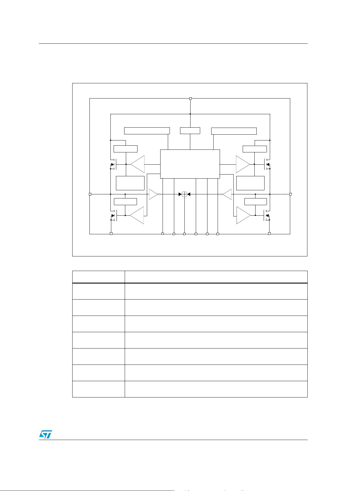
1 Block diagram and pin description
Figure 1. Block diagram
V
CC
OVERTEMPERATURE A
CLAMP HS
HS
A
OUT
A
CLAMP LS
LS
A
GND
A
Table 2. Block description
A
DRIVER
CURRENT
LIMITATION A
A
DRIVER
HS
A
LS
A
Name Description
Logic control
Allows the turn-on and the turn-off of the high-side and the low-side switches
according to the truth table
1/K
DIAGA/EN
OV + U
V
LOGIC
IN
CS DIAGB/EN
A
PWM
A
OVERTEMPERATURE B
1/K
IN
B
B
CLAMP HS
DRIVER
HS
B
CURRENT
LIMITATION B
CLAMP LS
DRIVER
LS
B
B
B
GND
HS
B
OUT
B
LS
B
B
Overvoltage +
undervoltage
High-side and lowside clamp voltage
High-side and lowside driver
Linear current limiter
Overtemperature
protection
Fault detection
Shuts down the device outside the range [5.5V..16V] for the battery voltage
Protect the high-side and the low-side switches from the high voltage on the
battery line in all configurations for the motor
Drives the gate of the concerned switch to allow a good R
for the leg of
DS(on)
the bridge
Limits the motor current by reducing the high-side switch gate source voltage
when short-circuit to ground occurs
In case of short-circuit with the increase of the junction’s temperature, shuts
down the concerned high side to prevent its degradation and to protect the die
Signals an abnormal behavior of the switches in the half-bridge A or B by
pulling low the concerned EN
/DIAGx pin
x
5/33
Block diagram and pin description VNH3ASP30-E
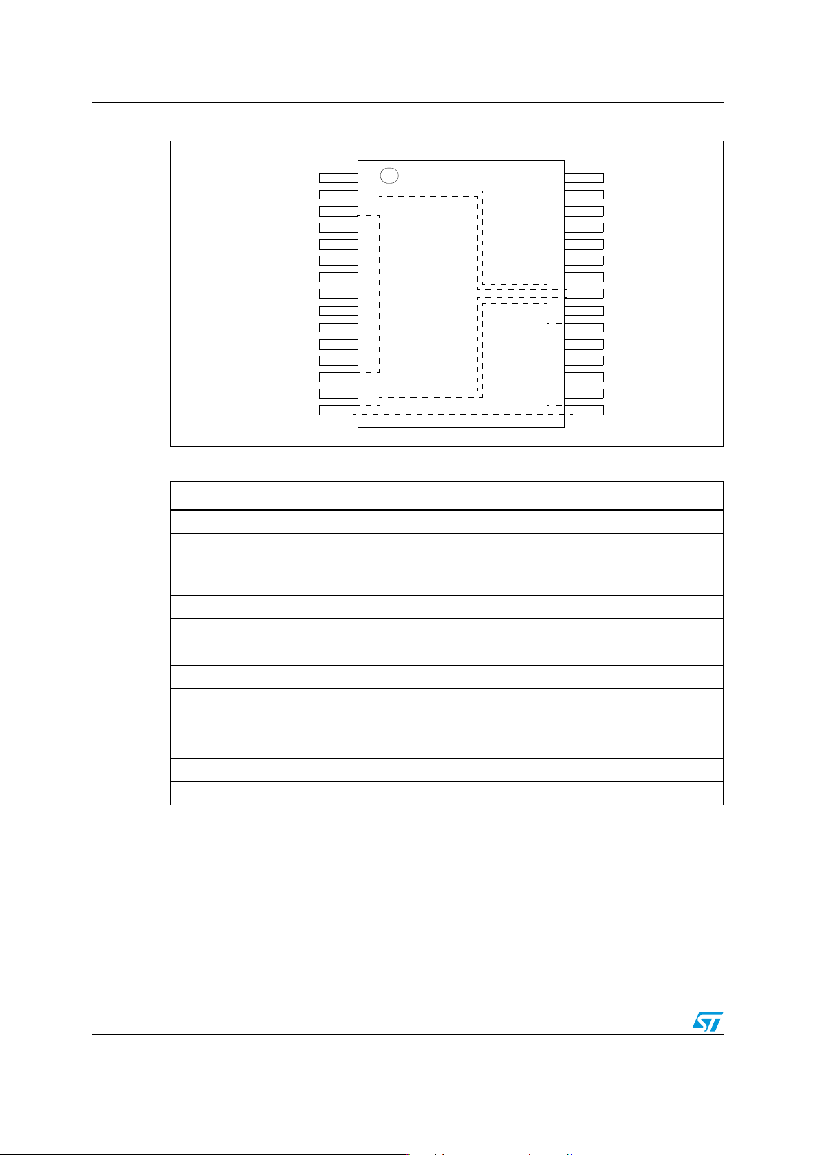
Figure 2. Configuration diagram (top view)
OUT
V
IN
ENA/DIAG
PWM
A
Nc
CC
Nc
A
A
Nc
1
OUT
Heat Slug3
V
CC
Heat Slug1
CS
EN
/DIAG
B
B
IN
B
Nc
V
CC
OUT
Heat Slug2
Nc
OUT
Table 3. Pin definitions and functions
15 16
B
Pin No. Symbol Function
1, 25, 30 OUT
2, 4, 7, 12, 14,
17, 22, 24, 29
, Heat Slug3 Source of high-side switch A / Drain of low-side switch A
A
NC Not connected
30
OUT
A
A
Nc
GND
GND
GND
OUT
A
A
A
A
Nc
V
CC
Nc
OUT
B
GND
B
B
GND
GND
B
B
Nc
OUT
B
3, 13, 23 VCC, Heat Slug1 Drain of high-side switches and power supply voltage
5IN
6EN
A
A
/DIAG
A
Clockwise input
Status of high-side and low-side switches A; open drain output
8 PWM PWM input
9 CS Output of current sense
10 EN
11 IN
15, 16, 21 OUT
26, 27, 28 GND
18, 19, 20 GND
/DIAG
B
B
B
, Heat Slug2 Source of high-side switch B / Drain of low-side switch B
B
A
B
1. GNDA and GNDB must be externally connected together.
Status of high-side and low-side switches B; open drain output
Counter clockwise input
Source of low-side switch A
Source of low-side switch B
(1)
(1)
6/33
VNH3ASP30-E Block diagram and pin description
Table 4. Pin functions description
Name Description
V
CC
, GNDBPower grounds; must always be externally connected together
GND
A
OUTBPower connections to the motor
OUT
A,
Battery connection
Voltage controlled input pins with hysteresis, CMOS compatible: These two pins
IN
A, INB
control the state of the bridge in normal operation according to the truth table (brake
to VCC, brake to GND, clockwise and counterclockwise).
Voltage controlled input pin with hysteresis, CMOS compatible: Gates of low-side
PWM
FETs are modulated by the PWM signal during their ON phase allowing speed
control of the motor.
Open drain bidirectional logic pins. These pins must be connected to an external pull
ENA/DIAGA,
ENB/DIAG
up resistor. When externally pulled low, they disable half-bridge A or B. In case of
fault detection (thermal shutdown of a high-side FET or excessive ON state voltage
B
drop across a low-side FET), these pins are pulled low by the device (see truth table
in fault condition).
Analog current-sense output. This output sources a current proportional to the motor
CS
current. The information can be read back as an analog voltage across an external
resistor.
7/33

Electrical specifications VNH3ASP30-E
2 Electrical specifications
Figure 3. Current and voltage conventions
I
S
V
I
INA
I
INB
I
ENA
I
ENB
V
INA
V
INB
V
ENA
V
ENB
IN
A
IN
B
DIAGA/EN
DIAGB/EN
PWM
I
pw
V
pw
V
CC
OUT
A
OUT
B
A
B
GND
CS
GND
A
B
V
SENSE
I
SENSE
I
V
OUTB
OUTB
I
OUTA
V
OUTA
GND
I
GND
CC
2.1 Absolute maximum ratings
Table 5. Absolute maximum ratings
Symbol Parameter Value Unit
Supply voltage +41 V
CC
Maximum output current (continuous) 30
Reverse output current (continuous) -30
I
R
Input current (INA and INB pins) ±10
I
IN
Enable input current (DIAGA/ENA and DIAGB/ENB pins) ±10
EN
PWM input current ±10
PW
Current-sense maximum voltage -3/+15 V
CS
Electrostatic discharge (R = 1.5kΩ, C = 100pF)
–CS pin
ESD
– logic pins
– output pins: OUT
Junction operating temperature Internally limited
T
J
Case operating temperature -40 to 150
C
Storage temperature -55 to 150
stg
, OUTB, V
A
CC
V
V
I
max
I
V
T
A
mAI
2
4
5
kV
kV
kV
°CT
8/33
VNH3ASP30-E Electrical specifications
2.2 Electrical characteristics
VCC = 9V up to 16 V; -40°C < TJ < 150°C, unless otherwise specified.
Table 6. Power section
Symbol Parameter Test conditions Min Typ Max Unit
V
Operating supply
CC
voltage
Off state:
= INB = PWM = 0; TJ = 25°C; VCC = 13V
IN
A
= INB = PWM = 0;
I
S
Supply current
IN
A
On state:
or INB = 5V, no PWM 10 mA
IN
A
= 12A; TJ = 25°C
R
ONHS
R
ONLS
Static high-side
resistance
Static low-side
resistance
I
OUT
= 12A; TJ = -40 to 150°C
I
OUT
= 12A TJ = 25°C
I
OUT
= 12A; TJ = -40 to 150°C
I
OUT
High-side
V
freewheeling diode
f
= 12A 0.8 1.1 V
I
f
forward voltage
I
L(off)
I
RM
High-side off-state
output current
(per channel)
Dynamic crossconduction current
TJ = 25°C; V
= 125°C; V
T
J
= 12A (see Figure 7)1.7A
I
OUT
=ENX=0V; VCC=13V 3
OUTX
=ENX=0V; VCC= 13V 5
OUTX
Table 7. Logic inputs (INA, INB, ENA, ENB)
5.5 16 V
12 30 60µA
µA
30
mΩ
60
12
mΩ
24
µA
Symbol Parameter Test conditions Min Typ Max Unit
V
V
V
I
I
V
Input low-level voltage
V
IL
Input high-level voltage 3.25
IH
Input hysteresis voltage 0.5
Ihys
Input clamp voltage
ICL
Input low current VIN = 1.25 V 1
INL
Input high current VIN = 3.25V 10
INH
Enable output low-level
DIAG
voltage
Normal operation (DIAG
/ENX pin acts
X
as an input pin)
I
= 1mA 5.5 6.3 7.5
IN
I
= -1mA -1.0 -0.7 -0.3
IN
Fault operation (DIAGX/ENX pin acts as
an output pin); IEN = 1mA
1.25
V
µA
0.4 V
9/33
Electrical specifications VNH3ASP30-E
Table 8. PWM
Symbol Parameter Test conditions Min Typ Max Unit
V
I
PWL
V
PWH
I
PWH
V
PWhys
V
PWCL
C
INPW
Table 9. Switching (VCC=13V, R
PWM low-level voltage 1.25 V
PWL
PWM low-level pin
current
V
= 1.25 V 1 µA
pw
PWM high-level voltage 3.25 V
PWM high-level pin
current
V
= 3.25V 10 µA
pw
PWM hysteresis voltage 0.5
I
= 1mA VCC+0.3 VCC+0.7 VCC+1.0
PWM clamp voltage
PWM pin input
capacitance
pw
= -1mA -6.0 -4.5 -3.0
I
pw
= 2.5V 25 pF
V
IN
= 1 Ω )
LOAD
Symbol Parameter Test conditions Min Typ Max Unit
f
t
d(on)
t
d(off)
t
DEL
PWM frequency 0 20 kHz
PW
Turn-on delay time
Turn-off delay time
t
Rise time (see Figure 5)11.6
r
Fall time (see Figure 5)12.4
t
f
Delay time during change
of operating mode
Input rise time < 1µs
(see Figure 6)
Input rise time < 1µs
(see Figure 6)
250
250
(see Figure 4) 300 600 1800
High-side freewheeling
diode reverse recovery
t
rr
(see Figure 7)110ns
time
Table 10. Protection and diagnostic
V
µs
Symbol Parameter Test conditions Min Typ Max Unit
V
UV(sd)
UV(reset)
V
OV(sd)
I
LIM
V
CLP
T
th(sd)
h(reset)
T
th(hys)
Undervoltage shutdown 5.5
Undervoltage reset 4.7
Overvoltage shutdown 16 19 22
High-side current limitation 30 50 70 A
Total clamp voltage (VCC to GND) I
Thermal shutdown temperature V
Thermal reset temperature 135
Thermal hysteresis 7 15
10/33
= 12A 43 48 54 V
OUT
= 3.25V 150 175 200
IN
VV
°CT
 Loading...