


VND810MSP-E
1
1
DOUBLE CHANNEL HIGH SIDE DRIVER
Table 1. General Features
Type R
VND810MSP-E 150 mΩ (*) 0.6 A (*) 36 V
(*) Per each channel
CMOS COMPATIBLE INPUTS
■
■ OPEN DRAIN STATUS OUTPUTS
■ ON STATE OPEN LOAD DETECTION
■ OFF STATE OPEN LOAD DETECTION
■ SHORTED LOAD PROTECTION
■ UNDERVOLTAGE AND OVERVOLTAGE
DS(on)
I
out
V
CC
SHUTDOWN
■ PROTECTION AGAINST LOSS OF GROUND
■ VERY LOW STAND-BY CURRENT
■ REVERSE BATTERY PROTECTION (**)
■ IN COMPLIANCE WITH THE 2002/95/EC
EUROPEAN DIRECTIVE
DESCRIPTION
The VND810MSP-E is a monolithic device
designed in STMicroelectronics VIPower M0-3
Technology, intended fo r driving any kind of load
with one side connected to ground.
Active V
pin voltage clamp protects the dev ice
CC
against low energy spikes (see ISO7637 transient
compatibility table).
Figure 1. Package
0
PowerSO-10™
Active current limitation combined with thermal
shutdown and automatic restart protects the
device against overload. The current limitation
threshold is aimed at detecting the 21W/12V
standard bulb as an overload fault. The device
detects open load condition both in on and off
state. Output shorted to V
is detected in the off
CC
state. Device automatically turns off in case of
ground pin disconnection.
Table 2. Order Codes
Package Tube Tape and Reel
PowerSO-10™ VND810MSP-E VND810MSPTR-E
Note: (**) See application schematic at page 9
Rev. 2
1/20March 2005
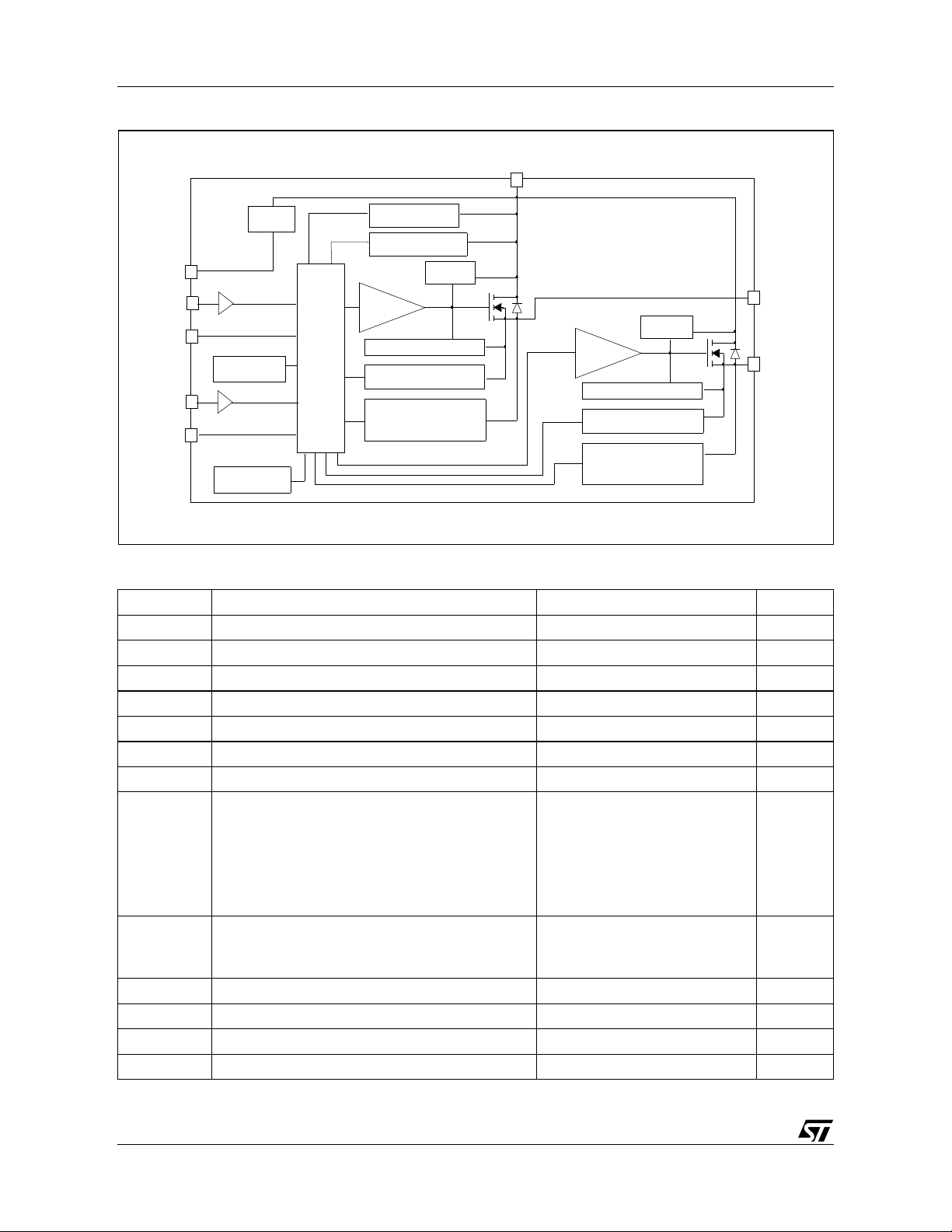
VND810MSP-E
Figure 2. Block Diagram
V
cc
CLAMP
OVERVOLTAGE
UNDERVOLTAGE
GND
INPUT1
STATUS1
INPUT2
STATUS2
OVERTEMP. 1
OVERTEMP. 2
LOGIC
DRIVER 1
CURRENT LIMITER 1
OPENLOAD ON 1
OPENLOAD OFF 1
CLAMP 1
CLAMP 2
DRIVER 2
CURRENT LIMITER 2
OPENLOAD ON 2
OPENLOAD OFF 2
Table 3. Absolute Maximum Ratings
Symbol Parameter Value Unit
DC Supply Voltage 41 V
Reverse DC Supply Vo lta ge - 0.3 V
DC Reverse Ground Pin Current - 200 mA
DC Output Current Internally Limited A
Reverse DC Output Cu rre nt - 6 A
DC Input Current +/- 10 mA
DC Status Current +/- 10 mA
Electrostatic Discharge (Human Body Model:
R=1.5KΩ; C=100pF)
- INPUT
- STATUS
- OUTPUT
- V
CC
4000
4000
5000
5000
Maximum Switching Energy
(L=400mH; R
I
=0.9A)
L
=0Ω; V
L
=13.5V; T
bat
jstart
=150ºC;
225 mJ
Power Dissipation TC=25°C 52 W
Junction Operating Temperature Internally Limited °C
Case Operating Temperature - 40 to 150 °C
Storage Temperature - 55 to 150 °C
- V
- I
- I
V
E
V
CC
GND
I
OUT
OUT
I
IN
I
stat
ESD
MAX
P
T
T
T
stg
CC
tot
j
c
OUTPUT1
OUTPUT2
V
V
V
V
2/20

VND810MSP-E
Figure 3. Configuration Diagram (Top View) & Suggested Connections for Unused and N.C. Pins
GROUND
INPUT 1
STA TUS 1
STA TUS 2
INPUT 2
V
CC
Connection / Pin Status N.C. Output Input
Floating X X X X
To Ground X Through 10KΩ resistor
Figure 4. Current and Voltage Conventions
I
IN1
I
V
IN1
V
STAT1
STAT1
I
IN2
I
V
STAT2
IN2
V
STAT2
INPUT 1
STATUS 1
INPUT 2
STATUS 2
6
7
8
9
10
11
5
4
3
2
1
V
CC
OUTPUT 1
OUTPUT 1
N.C.
OUTPUT 2
OUTPUT 2
V
(*)
F1
I
OUT1
I
S
V
CC
OUTPUT 1
V
OUT1
I
OUT2
V
OUT2
GND
OUTPUT 2
I
GND
(*) VFn = V
CCn
- V
during reverse battery condition
OUTn
Table 4. Thermal Data
Symbol Parameter Value Unit
R
thj-case
R
thj-amb
Note: 1. When mounted on a standard single-side d FR-4 board with 0.5 c m2 of Cu (at least 35µm thick). Hori zontal mounti ng and no arti ficial
Note: 2. When mounted on a standard single-sided FR-4 board with 6 cm
Thermal Resistance Junction-case 2.4 °C/W
Thermal Resistance Junction-ambient 52.4
air flow.
air flow.
2
of Cu (at least 3 5µm thick). Horizontal mounting and no artificial
(1)
37
(2)
°C/W
3/20
VND810MSP-E
ELECTRICAL CHARACTERISTICS
(8V<V
(Per each channel)
Table 5. Power Outputs
Symbol Parameter Test Conditions Min Typ Max Unit
V
V
V
Note: (**) Per device.
<36V; -40°C<Tj<150°C; unless otherwise specified)
CC
(**) Operating Supply Voltage 5.5 13 36 V
CC
(**) Undervoltage Shut-down 3 4 5.5 V
USD
(**) Over vo ltag e Sh ut- do wn 36 V
OV
R
ON
On State Resistance
IS (**) Supply Current
I
L(off1)
I
L(off2)
I
L(off3)
I
L(off4)
Off State Output Current VIN=V
Off State Output Current VIN=0V; V
Off State Output Current VIN=V
Off State Output Current VIN=V
I
=0.5A; Tj=25°C
OUT
=0.5A; VCC>8V
I
OUT
Off State; V
Off State; V
Tj=25°C
On State; V
OUT
OUT
OUT
=13V; VIN=V
CC
=13V; VIN=V
CC
OUT
OUT
=0V
=0V;
12
12
=13V; VIN=5V; I
CC
OUT
=0A
5
=0V 0 50 µA
=3.5V -75 0 µA
OUT
=0V; VCC=13V; Tj =125°C 5 µA
=0V; VCC=13V; Tj =25°C 3 µA
150
320
40
25
7
mΩ
mΩ
µA
µA
mA
Table 6. Protection (See note 1)
Symbol Parameter Test Conditions Min . Typ. Max. Un it
T
TSD
T
T
hyst
t
SDL
I
lim
V
demag
Note: 1. To ensure long term reliability under heavy overload or short circuit conditions, protection and related diagnostic signals must be
Shut-down Temp era tu re 150 175 200 °C
Reset Temperature 135 °C
R
Thermal Hysteres is 7 15 °C
Status Delay in Overload
Conditions
Current limitation
Turn-off Output Cla mp
Voltage
used together with a proper software strategy. If the dev ice is subjected to abn ormal conditions , this software must limit the duration
and number of activation cycles
Tj>T
TSD
0.6 0.9 1.2
5.5V<V
I
OUT
<36V
CC
=0.5A; L=6mH VCC-41 VCC-48 VCC-55 V
20 µs
1.2
A
A
Table 7. VCC - Output Diode
Symbol Parameter Test Conditions M in T yp Max Unit
V
Forward on Voltage -I
F
=0.5A; Tj=150°C 0.6 V
OUT
4/20

VND810MSP-E
ELECTRICAL CHARACTERISTICS (continued)
Table 8. Status Pin
Symbol Parameter Test Conditions M in Typ Max Unit
V
STAT
I
LSTAT
C
STAT
V
SCL
Status Low Output Voltage I
= 1.6 mA 0.5 V
STAT
Status Leakage Current Normal Operation; V
Status Pin Input
Capacitance
Status Clamp Voltag e
Normal Operation; V
I
= 1mA
STAT
= - 1mA
I
STAT
= 5V 10 µA
STAT
= 5V 100 pF
STAT
66.8
-0.7
8V
V
Table 9. Switching (V
CC
=13V)
Symbol Parameter Test Conditions Min Typ Max Unit
R
=13Ω from VIN rising edge to
L
V
=1.3V
OUT
R
=13Ω from VIN falling edge to
L
V
=11.7V
OUT
=13Ω from V
R
L
V
=10.4V
OUT
=13Ω from V
R
L
V
=1.3V
OUT
=1.3V to
OUT
=11.7V to
OUT
30 µs
30 µs
See
relative
diagram
See
relative
diagram
dV
dV
t
d(on)
t
d(off)
OUT
OUT
Turn-on Delay Time
Turn-off Delay Time
/dt
Turn-on Voltage Slope
(on)
/dt
Turn-off Voltage Slope
(off)
Table 10. Openload Detection
Symbol Parameter Test Conditions Min Typ Max Unit
I
OL
t
DOL(on)
V
OL
t
DOL(off)
Openload ON State
Detection Thresho ld
Openload ON State
Detection Delay
Openload OFF State
Voltage Detection
Threshold
Openload Detection Delay
at Turn Off
=5V 20 40 80 mA
V
IN
=0A 200 µs
I
OUT
V
=0V 1.5 2.5 3.5 V
IN
1000 µs
V/µs
V/µs
Table 11. Logic Input
Symbol Parameter Test Conditions Min Typ Max Unit
V
V
V
I
V
I
IH
I(hyst)
ICL
Input Low Level 1.25 V
IL
Low Level Input Current VIN = 1.25V 1 µA
IL
Input High Level 3.25 V
IH
High Level Input Current VIN = 3.25V 10 µA
Input Hysteresis Voltage 0.5 V
Input Clamp Voltage
I
= 1mA
IN
= -1mA
I
IN
66.8
-0.7
8V
V
5/20

VND810MSP-E
Figure 5.
OPEN LOAD STATUS TIMING (with external pull-up)
V
> V
OUT
OL
V
INn
V
STAT n
t
DOL(off)
Table 12. Truth Table
CONDITIONS INPUT OUTPUT SENSE
Normal Operation
Current Limitation
Overtemperature
Undervoltage
Overvoltage
Output Voltage > V
Output Current < I
OL
OL
L
H
L
H
H
L
H
L
H
L
H
L
H
L
H
I
OUT
t
DOL(on)
< I
OVER TEMP STATUS TIMING
OL
V
INn
V
STAT n
L
H
L
X
X
L
L
L
L
L
L
H
H
L
H
t
SDL
Tj > T
(T
(T
TSD
< T
j
> T
j
TSD
TSD
t
SDL
) H
) L
H
H
H
H
L
X
X
H
H
L
H
H
L
6/20
 Loading...