

Features
VND7N04, VND7N04-1
VNK7N04FM
"OMNIFET":
Fully autoprotected power MOSFET
Type V
VND7N04
VND7N04-1
VNK7N04FM
■
Linear current limitation
■
Thermal shut down
■
Short circuit protection
■
Integrated clamp
■
Low current drawn from input pin
■
Diagnostic feedback through input pin
■
ESD protection
■
Direct access to the gate of the power
clamp
42 V
42 V
42 V
R
DS(on)
0.14 Ω
0.14 Ω
0.14 Ω
MOSFET (analog driving)
■
Compatible with standard power MOSFET
I
lim
7 A
7 A
7 A
Description
The VND7N04, VND7N04-1 and VNK7N04FM
are monolithic devices made using
STMicroeletronics VIPower M0 Technology,
intended for replacement of standard power
MOSFETS in DC to 50 KHz applications. Built-in
thermal shut-down, linear current limitation and
overvoltage clamp protect the chip in harsh
enviroments.
Fault feedback can be detected by monitoring the
voltage at the input pin.
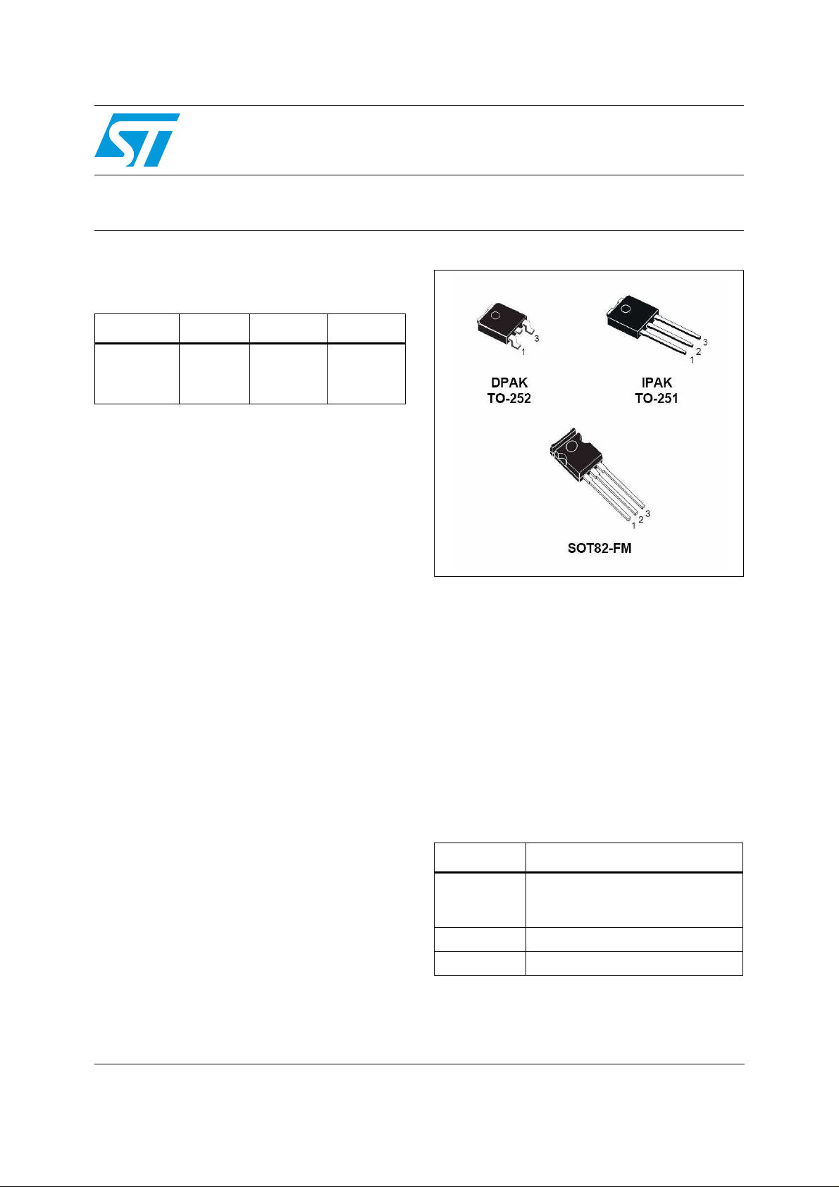
Table 1. Device summary
Part number Order code
VND7N04, VND7N04-1-E,
VND7N04
VND7N04-1 VND7N04-1
VNK7N04FM VNK7N04FM
March 2009 Rev 1 1/17
VND7N04-E, VND7N0413TR,
VND7N04TR-E
www.st.com
17

Contents VND7N04, VND7N04-1, VNK7N04FM
Contents
1 Block diagram . . . . . . . . . . . . . . . . . . . . . . . . . . . . . . . . . . . . . . . . . . . . . . 3
2 Electrical specification . . . . . . . . . . . . . . . . . . . . . . . . . . . . . . . . . . . . . . . 4
2.1 Absolute maximum rating . . . . . . . . . . . . . . . . . . . . . . . . . . . . . . . . . . . . . . 4
2.2 Thermal data . . . . . . . . . . . . . . . . . . . . . . . . . . . . . . . . . . . . . . . . . . . . . . . 4
2.3 Electrical characteristics . . . . . . . . . . . . . . . . . . . . . . . . . . . . . . . . . . . . . . . 4
3 Protection features . . . . . . . . . . . . . . . . . . . . . . . . . . . . . . . . . . . . . . . . . . 7
4 Package information . . . . . . . . . . . . . . . . . . . . . . . . . . . . . . . . . . . . . . . . 13
5 Revision history . . . . . . . . . . . . . . . . . . . . . . . . . . . . . . . . . . . . . . . . . . . 16
2/17
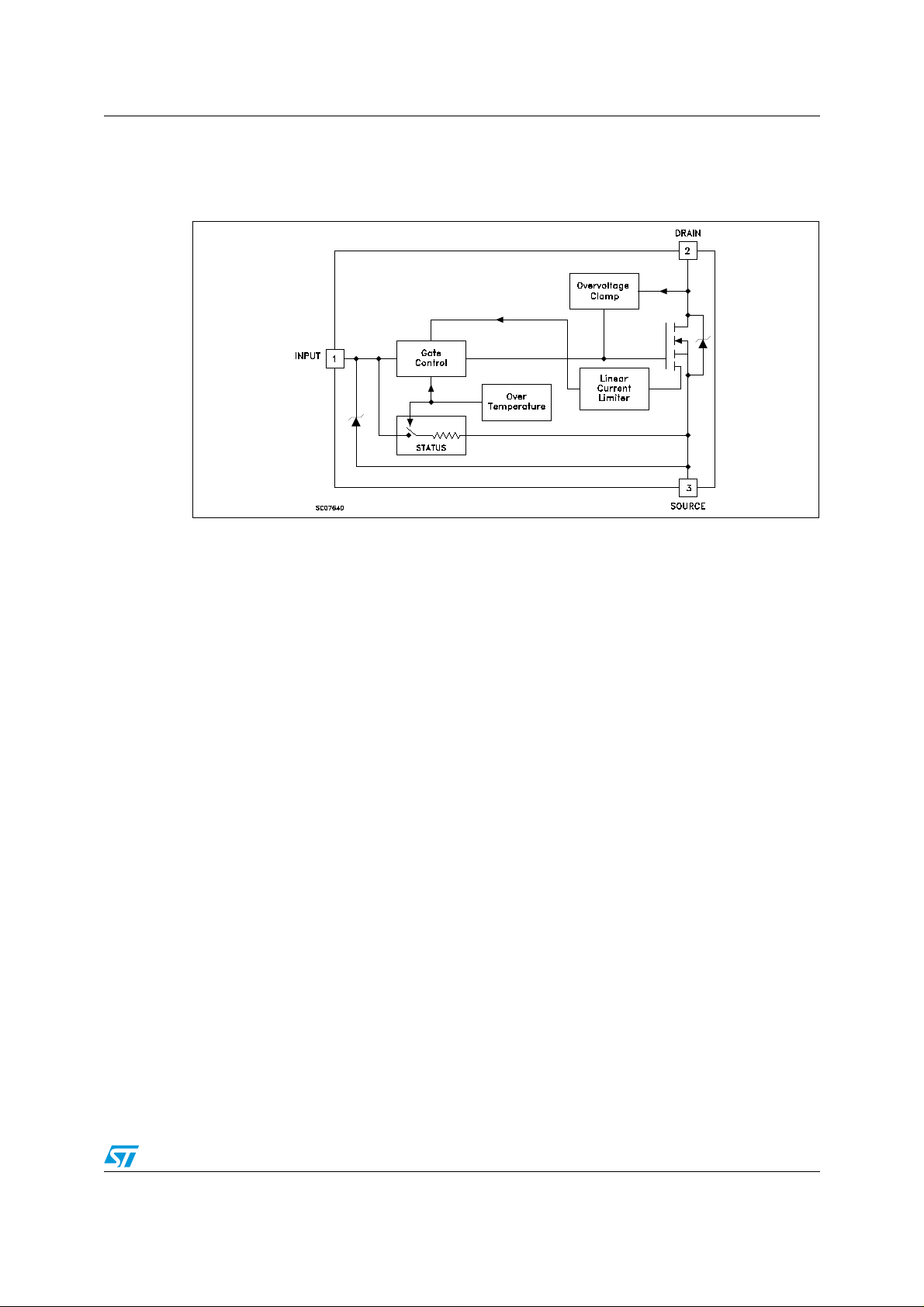
VND7N04, VND7N04-1, VNK7N04FM Block diagram
1 Block diagram
Figure 1. Block diagram
3/17
Electrical specification VND7N04, VND7N04-1, VNK7N04FM
2 Electrical specification
2.1 Absolute maximum rating
Table 2. Absolute maximum rating
Value
Symbol Parameter
V
DS
V
I
D
I
R
V
esd
P
tot
T
T
T
stg
Drain-source voltage (Vin = 0) Internally clamped V
in
Input voltage 18 V
Drain current Internally limited A
Reverse DC output current -7 A
Electrostatic discharge (C = 100 pF,
R=1.5 KΩ)
Total dissipation at Tc = 25 °C 60 9 W
j
Operating junction temperature Internally limited °C
c
Case operating temperature Internally limited °
Storage temperature -55 to 150 °
2.2 Thermal data
Table 3. Thermal data
R
thj-case
R
thj-amb
Thermal resistance junction-case max 3.75 14 °C/W
Thermal resistance junction-ambient max 100 100 °C/W
DPAK
IPAK
SOT-82FM
2000 V
DPAK/IPAK SOT82-FM
Unit
C
C
2.3 Electrical characteristics
Table 4. Electrical characteristics: off
Symbol Parameter Test conditions Min. Typ. Max. Unit
V
CLAMP
V
CLTH
V
INCL
I
DSS
I
ISS
4/17
(-40 < Tj < 125 °C unless otherwise specified)
Drain-source clamp voltage ID = 200 mA Vin = 0 32 42 52 V
Drain-source clamp threshold voltage ID = 2 mA Vin = 0 31 V
Input-source reverse clamp voltage Iin = -1 mA -1.1 -0.25 V
Zero input voltage drain current (Vin = 0)
VDS = 13 V Vin = 0
VDS = 25 V Vin = 0
Supply current from input pin VDS = 0 V Vin = 10 V 250 550 µA
75
200
µA
µA
VND7N04, VND7N04-1, VNK7N04FM Electrical specification
Table 5. Electrical characteristics: on
Symbol Parameter Test conditions Min. Typ. Max. Unit
V
IN(th)
R
DS(on)
Input threshold voltage VDS = Vin ID + Iin = 1 mA 0.8 3 V
Static drain-source on resistance
Vin = 10 V ID = 3.5 A
Vin = 5 V ID = 3.5 A
-40 < Tj < 25 °C
Vin = 10 V ID = 3.5 A
Vin = 5 V ID = 3.5 A
0.14
0.28
0.28
0.56
Tj = 125 °C
Table 6. Electrical characteristics: dynamic
Symbol Parameter Test conditions Min. Typ. Max. Unit
gfs
C
oss
1. Pulsed: Pulse duration = 300 µs, duty cycle 1.5 %
Table 7. Electrical characteristics: switching
transconductance
Output capacitance VDS = 13 V f = 1 MHz Vin = 0 250 500 pF
VDS = 13 V ID = 3.5 A 2 5 S
Forward
(1)
Symbol Parameter Test conditions Min. Typ. Max. Unit
Ω
Ω
Ω
Ω
td(on)
t
td(off)
t
td(on)
t
td(off)
t
(di/dt)on Turn-on current slope
Q
Table 8. Electrical characteristics: source drain diode
Turn-on delay time
Rise time
r
Turn-off delay time
Fall time
f
Turn-on delay time
Rise time
r
Turn-off delay time
Fall time
f
Total input charge VDD = 12 V ID = 3.5 A Vin = 10 V 18 nC
i
VDD = 15 V Id = 3.5 A
V
= 10 V R
gen
gen
= 10 Ω
(see Figure 26)
VDD = 15 V Id = 3.5 A
V
= 10 V R
gen
= 1000 Ω
gen
(see Figure 26)
VDD = 15 V ID = 3.5 A
Vin = 10 V R
gen
= 10 Ω
50
60
130
50
140
0.4
2.5
1
50 A/µs
150
180
300
200
500
1.1
7
4
Symbol Parameter Test conditions Min. Typ. Max. Unit
(1)
VSD
trr
Qrr
I
RRM
1. Pulsed: Pulse duration = 300 µs, duty cycle 1.5 %
2. Parameters guaranteed by design/characterization
Forward on voltage ISD = 3.5 A Vin = 0 1.7 V
(2)
Reverse recovery time
(2)
Reverse recovery charge
(2)
Reverse recovery current
ISD = 3.5 A di/dt = 100 A/µs
VDD = 30 V Tj = 25 °C
(see test circuit, Figure 28)
40
0.2
3.6
ns
ns
ns
ns
ns
µs
µs
µs
ns
µC
A
5/17
Electrical specification VND7N04, VND7N04-1, VNK7N04FM
Table 9. Electrical characteristics: protection
Symbol Parameter Test conditions Min. Typ. Max. Unit
I
lim
t
dlim
T
jsh
T
jrs
I
gf
Eas
1. Pulsed: Pulse duration = 300 µs, duty cycle 1.5 %
Drain current limit
Step response
(1)
Current limit
Overtemperature
(1)
shutdown
(1)
Overtemperature reset 135 °
(1)
Fault sink current
Single pulse avalanche
(1)
energy
Vin = 10 V VDS = 13 V
Vin = 5 V VDS = 13 V
Vin = 10 V
Vin = 5 V
Vin = 10 V VDS = 13 V
Vin = 5 V VDS = 13 V
starting Tj = 25°C VDD = 20 V
Vin = 10 V R
= 1 KΩ L = 30 mH
gen
4
4
13
15
7
7
11
11
20
25
150 °C
50
20
mA
mA
0.4 J
A
A
µs
µs
C
6/17
 Loading...