

Features
VND5N07
OMNIFET II
fully autoprotected Power MOSFET
Max. on-state resistance (per ch.) R
Current limitation (typ) I
Drain-Source clamp voltage V
■ Linear current limitation
■ Thermal shutdown
■ Short circuit protection
■ Integrated clamp
■ Low current drawn from input pin
■ Diagnostic feedback through input pin
■ Esd protection
■ Direct access to the gate of the power mosfet
DS (on)
LIMH
CLAMP
0.2Ω
5 A
70V
(analog driving)
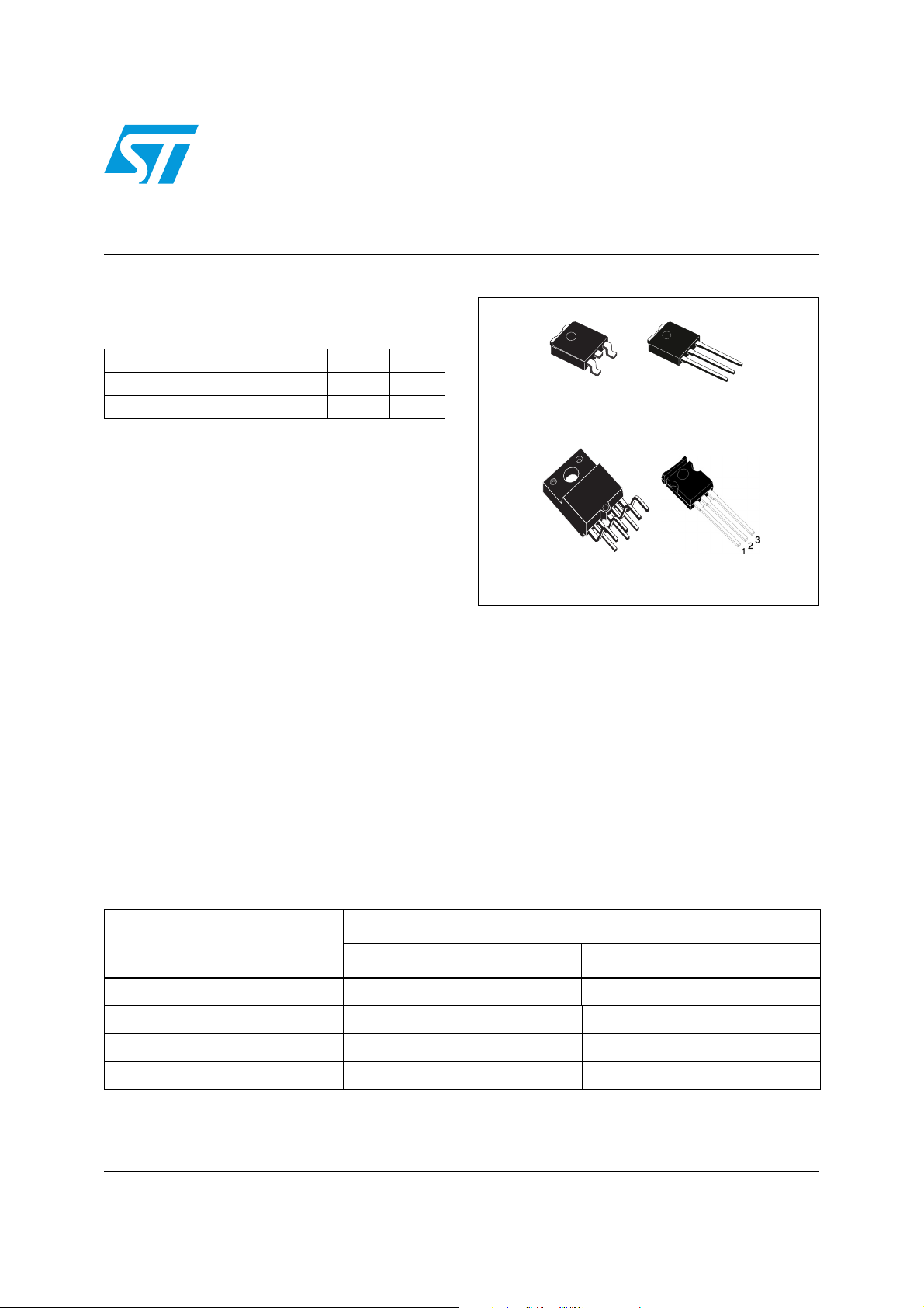
■ Compatible with standard Power MOSFET
DPAK
TO-252
3
1
IPAK
TO-251
3
2
1
ISOWATT200
SOT-82FM
Description
The VND5N07 is a monolithic device designed in
STMicroelectronics VIPower M0 technology,
intended for replacement of standard Power
MOSFETs from DC to 50KHz applications. Built in
thermal shutdown, linear current limitation and
overvoltage clamp protect the chip in harsh
environments.
Fault feedback can be detected by monitoring the
voltage at the input pin.
Table 1. Device summary
Order codes
Package
Tube Tape and reel
DPAK VND5N07 VND5N0713TR
IPAK VND5N07-1
ISOWATT220 VNP5N07FI
SOT-82FM VNK5N07FM
December 2008 Rev 3 1/24
www.st.com
24

Contents VND5N07
Contents
1 Block diagram and pin description . . . . . . . . . . . . . . . . . . . . . . . . . . . . . 5
2 Electrical specifications . . . . . . . . . . . . . . . . . . . . . . . . . . . . . . . . . . . . . . 6
2.1 Absolute maximum ratings . . . . . . . . . . . . . . . . . . . . . . . . . . . . . . . . . . . . . 6
2.2 Thermal data . . . . . . . . . . . . . . . . . . . . . . . . . . . . . . . . . . . . . . . . . . . . . . . 6
2.3 Electrical characteristics . . . . . . . . . . . . . . . . . . . . . . . . . . . . . . . . . . . . . . . 7
2.4 Electrical characteristics curves . . . . . . . . . . . . . . . . . . . . . . . . . . . . . . . . 13
3 Protection features . . . . . . . . . . . . . . . . . . . . . . . . . . . . . . . . . . . . . . . . . 17
3.1 Overvoltage clamp protection . . . . . . . . . . . . . . . . . . . . . . . . . . . . . . . . . . 17
3.2 Linear current limiter circuit . . . . . . . . . . . . . . . . . . . . . . . . . . . . . . . . . . . 17
3.3 Overtemperature and short circuit protection . . . . . . . . . . . . . . . . . . . . . . 17
3.4 Status feedback . . . . . . . . . . . . . . . . . . . . . . . . . . . . . . . . . . . . . . . . . . . . 17
4 Package and packing information . . . . . . . . . . . . . . . . . . . . . . . . . . . . . 18
4.1 ECOPACK® packages . . . . . . . . . . . . . . . . . . . . . . . . . . . . . . . . . . . . . . . 18
4.2 DPAK mechanical data . . . . . . . . . . . . . . . . . . . . . . . . . . . . . . . . . . . . . . . 18
4.3 IPAK mechanical data . . . . . . . . . . . . . . . . . . . . . . . . . . . . . . . . . . . . . . . 20
4.4 ISOWATT220 mechanical data . . . . . . . . . . . . . . . . . . . . . . . . . . . . . . . . 21
4.5 SOT-82FM mechanical data . . . . . . . . . . . . . . . . . . . . . . . . . . . . . . . . . . . 22
5 Revision history . . . . . . . . . . . . . . . . . . . . . . . . . . . . . . . . . . . . . . . . . . . 23
2/24

VND5N07 List of tables
List of tables
Table 1. Device summary . . . . . . . . . . . . . . . . . . . . . . . . . . . . . . . . . . . . . . . . . . . . . . . . . . . . . . . . . . 1
Table 2. Absolute maximum ratings . . . . . . . . . . . . . . . . . . . . . . . . . . . . . . . . . . . . . . . . . . . . . . . . . . 6
Table 3. Thermal data. . . . . . . . . . . . . . . . . . . . . . . . . . . . . . . . . . . . . . . . . . . . . . . . . . . . . . . . . . . . . 6
Table 4. Off . . . . . . . . . . . . . . . . . . . . . . . . . . . . . . . . . . . . . . . . . . . . . . . . . . . . . . . . . . . . . . . . . . . . . 7
Table 5. On . . . . . . . . . . . . . . . . . . . . . . . . . . . . . . . . . . . . . . . . . . . . . . . . . . . . . . . . . . . . . . . . . . . . . 7
Table 6. Dynamic . . . . . . . . . . . . . . . . . . . . . . . . . . . . . . . . . . . . . . . . . . . . . . . . . . . . . . . . . . . . . . . . 7
Table 7. Switching . . . . . . . . . . . . . . . . . . . . . . . . . . . . . . . . . . . . . . . . . . . . . . . . . . . . . . . . . . . . . . . 8
Table 8. Source Drain diode . . . . . . . . . . . . . . . . . . . . . . . . . . . . . . . . . . . . . . . . . . . . . . . . . . . . . . . . 8
Table 9. Protections (-40°C < Tj < 150°C, unless otherwise specified) . . . . . . . . . . . . . . . . . . . . . . . 8
Table 10. DPAK mechanical data. . . . . . . . . . . . . . . . . . . . . . . . . . . . . . . . . . . . . . . . . . . . . . . . . . . . 19
Table 11. IPAK mechanical data . . . . . . . . . . . . . . . . . . . . . . . . . . . . . . . . . . . . . . . . . . . . . . . . . . . . 20
Table 12. ISOWATT220 mechanical data . . . . . . . . . . . . . . . . . . . . . . . . . . . . . . . . . . . . . . . . . . . . . 21
Table 13. SOT-82FM mechanical data . . . . . . . . . . . . . . . . . . . . . . . . . . . . . . . . . . . . . . . . . . . . . . . . 22
Table 14. Document revision history . . . . . . . . . . . . . . . . . . . . . . . . . . . . . . . . . . . . . . . . . . . . . . . . . 23
3/24

List of figures VND5N07
List of figures
Figure 1. Block diagram . . . . . . . . . . . . . . . . . . . . . . . . . . . . . . . . . . . . . . . . . . . . . . . . . . . . . . . . . . . . 5
Figure 2. Switching time test circuit for resistive load . . . . . . . . . . . . . . . . . . . . . . . . . . . . . . . . . . . . . 9
Figure 3. Test circuit for diode recovery times . . . . . . . . . . . . . . . . . . . . . . . . . . . . . . . . . . . . . . . . . . . 9
Figure 4. Unclamped inductive load test circuits . . . . . . . . . . . . . . . . . . . . . . . . . . . . . . . . . . . . . . . . 10
Figure 5. Input charge test circuit. . . . . . . . . . . . . . . . . . . . . . . . . . . . . . . . . . . . . . . . . . . . . . . . . . . . 10
Figure 6. Unclamped inductive waveforms . . . . . . . . . . . . . . . . . . . . . . . . . . . . . . . . . . . . . . . . . . . . 11
Figure 7. Switching waveforms . . . . . . . . . . . . . . . . . . . . . . . . . . . . . . . . . . . . . . . . . . . . . . . . . . . . . 11
Figure 8. Thermal impedance for ISOWATT220 . . . . . . . . . . . . . . . . . . . . . . . . . . . . . . . . . . . . . . . . 12
Figure 9. Thermal impedance for DPAK / IPAK. . . . . . . . . . . . . . . . . . . . . . . . . . . . . . . . . . . . . . . . . 12
Figure 10. Source-Drain diode forward characteristics . . . . . . . . . . . . . . . . . . . . . . . . . . . . . . . . . . . . 13
Figure 11. Static Drain-Source on resistance . . . . . . . . . . . . . . . . . . . . . . . . . . . . . . . . . . . . . . . . . . . 13
Figure 12. Derating curve . . . . . . . . . . . . . . . . . . . . . . . . . . . . . . . . . . . . . . . . . . . . . . . . . . . . . . . . . . 13
Figure 13. Static Drain-Source on resistance vs. input voltage . . . . . . . . . . . . . . . . . . . . . . . . . . . . . . 13
Figure 14. Normalized on resistance Vs temperature . . . . . . . . . . . . . . . . . . . . . . . . . . . . . . . . . . . . . 13
Figure 15. Transconductance . . . . . . . . . . . . . . . . . . . . . . . . . . . . . . . . . . . . . . . . . . . . . . . . . . . . . . . 13
Figure 16. Static Drain-Source on resistance Vs. Id . . . . . . . . . . . . . . . . . . . . . . . . . . . . . . . . . . . . . . 14
Figure 17. Switching time resistive load. . . . . . . . . . . . . . . . . . . . . . . . . . . . . . . . . . . . . . . . . . . . . . . . 14
Figure 18. Turn-on current slope . . . . . . . . . . . . . . . . . . . . . . . . . . . . . . . . . . . . . . . . . . . . . . . . . . . . . 14
Figure 19. Turn-on current slope . . . . . . . . . . . . . . . . . . . . . . . . . . . . . . . . . . . . . . . . . . . . . . . . . . . . . 14
Figure 20. Input voltage Vs. input charge . . . . . . . . . . . . . . . . . . . . . . . . . . . . . . . . . . . . . . . . . . . . . . 14
Figure 21. Turn-off Drain source voltage slope . . . . . . . . . . . . . . . . . . . . . . . . . . . . . . . . . . . . . . . . . . 14
Figure 22. Turn-off Drain-Source voltage slope . . . . . . . . . . . . . . . . . . . . . . . . . . . . . . . . . . . . . . . . . . 15
Figure 23. Capacitance variations . . . . . . . . . . . . . . . . . . . . . . . . . . . . . . . . . . . . . . . . . . . . . . . . . . . . 15
Figure 24. Switching time resistive load. . . . . . . . . . . . . . . . . . . . . . . . . . . . . . . . . . . . . . . . . . . . . . . . 15
Figure 25. Step response current limit . . . . . . . . . . . . . . . . . . . . . . . . . . . . . . . . . . . . . . . . . . . . . . . . . 15
Figure 26. Output characteristics . . . . . . . . . . . . . . . . . . . . . . . . . . . . . . . . . . . . . . . . . . . . . . . . . . . . . 15
Figure 27. Normalized on resistance Vs. temperature. . . . . . . . . . . . . . . . . . . . . . . . . . . . . . . . . . . . . 15
Figure 28. Normalized Input threshold voltage Vs. temperature . . . . . . . . . . . . . . . . . . . . . . . . . . . . . 16
Figure 29. Normalized current limit Vs. junction temperature . . . . . . . . . . . . . . . . . . . . . . . . . . . . . . . 16
Figure 30. DPAK package dimensions . . . . . . . . . . . . . . . . . . . . . . . . . . . . . . . . . . . . . . . . . . . . . . . . 18
Figure 31. IPAK mechanical data and package outline . . . . . . . . . . . . . . . . . . . . . . . . . . . . . . . . . . . . 20
Figure 32. ISOWATT220 mechanical data and package outline . . . . . . . . . . . . . . . . . . . . . . . . . . . . . 21
Figure 33. SOT-82FM mechanical data and package outline . . . . . . . . . . . . . . . . . . . . . . . . . . . . . . . 22
4/24
VND5N07 Block diagram and pin description
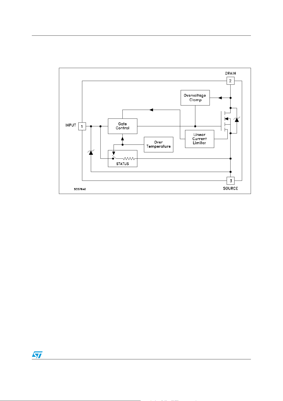
1 Block diagram and pin description
Figure 1. Block diagram
5/24
Electrical specifications VND5N07
2 Electrical specifications
2.1 Absolute maximum ratings
Stressing the device above the rating listed in the “Absolute maximum ratings” table may
cause permanent damage to the device. These are stress ratings only and operation of the
device at these or any other conditions above those indicated in the operating sections of
this specification is not implied. Exposure to Absolute maximum rating conditions for
extended periods may affect device reliability. Refer also to the STMicroelectronics SURE
program and other relevant quality document.
Table 2. Absolute maximum ratings
Symbol Parameter
DPAK / IPAK ISOWATT220 SOT-82FM
Value Un it
V
V
V
P
T
Drain-Source voltage (V
DSn
Input voltage 18 V
INn
I
Drain current Internally limited A
Dn
I
Reverse DC output current -7 A
Rn
Electrostatic discharge (R = 1.5KΩ,
ESD
C = 100pF)
Total dissipation at Tc = 25°C 60 24 9 W
tot
T
Operating junction temperature Internally limited °C
j
T
Case operating temperature Internally limited °C
c
Storage temperature -55 to 150 °C
stg
2.2 Thermal data
Table 3. Thermal data
Symbol Parameter
R
R
thj-case
thj-amb
Thermal resistance junction-case 3.75 5.2 14 °C/W
Thermal resistance junction-ambient 100 62.5 100 °C/W
= 0V) Internally clamped V
INn
2000 V
Max. value Unit
DPAK / IPAK ISOWATT220 SOT-82FM
6/24
VND5N07 Electrical specifications
2.3 Electrical characteristics
Tcase = 25°C unless otherwise stated.
Table 4. Off
Symbol Parameter Test conditions Min. Typ. Max. Unit
V
CLAMP
V
CLTH
I
V
I
DSS
Table 5. On
Drain-Source clamp
voltage
Drain-Source
threshold voltage
Supply current from
ISS
input pin
Input-Source reverse
INCL
clamp voltage
Zero input voltage
drain current
=0V)
(V
IN
(1)
V
= 0V; ID = 200mA 60 70 80 V
IN
= 0V; ID = 2mA 55 V
V
IN
= 0V; V
V
DS
I
= 1mA -1.0 -0.3 V
IN
V
= 13V; V
DS
= 25V; V
V
DS
= 10V 250 500 µA
IN
IN
IN
= 0V;
= 0V
50
200µAµA
Symbol Parameter Test conditions Min. Typ. Max. Unit
R
DS(on)
V
IN(th)
1. Pulsed: pulse duration = 300µs, duty cycle 1.5%.
Static Drain-Source
on resistance
Input threshold
voltage
V
IN
V
IN
= Vin; ID + Iin = 1 mA 0.8 3 V
V
DS
=10V; ID = 2.5A;
= 5V; ID = 2.5A
200
280
mΩ
Table 6. Dynamic
Symbol Parameter Test conditions Min. Typ. Max. Unit
Forward
(1)
g
fs
C
1. Pulsed: pulse duration = 300µs, duty cycle 1.5%.
transconductance
Output capacitance V
OSS
V
= 13V; ID = 2.5A 3 4 S
DS
= 13V; f = 1MHz; V
DS
= 0V 200 300 pF
IN
7/24
Electrical specifications VND5N07
Table 7. Switching
(1)
Symbol Parameter Test conditions Min. Typ. Max. Unit
t
d(on)
t
d(off)
t
d(on)
t
d(off)
(dI/dt)
1. Parameters guaranteed by design / characterization.
Turn-on delay time
Rise time 60 100 ns
t
r
Turn-off delay time 150 300 ns
t
Fall time 40 80 ns
f
= 15V; ID = 2.5A
V
DD
= 10V; R
V
gen
gen
= 10Ω
Turn-on delay time
Rise time 400 600 ns
t
r
Turn-off delay time 3900 5000 ns
Fall time 1100 1600 ns
t
f
Turn-on current slope
on
Total input charge V
Q
i
V
= 15V; ID = 2.5A
DD
V
= 10V; R
gen
V
= 15V; ID = 2.5A
DD
= 10V; R
V
in
= 12V; ID = 2.5A; V
DD
gen
gen
= 1kΩ
= 10Ω
= 10V 18 nC
IN
50 100 ns
150 250 ns
80 A/µS
Table 8. Source Drain diode
Symbol Parameter Test conditions Min. Typ. Max. Unit
(1)
V
SD
t
rr
Q
I
RRM
1. Pulsed: pulse duration = 300µs, duty cycle 1.5%.
2. Parameters guaranteed by design / characterization.
Table 9. Protections (-40°C < Tj < 150°C, unless otherwise specified)
Forward On voltage I
(2)
Reverse recovery time
Reverse recovery
(2)
rr
charge
Reverse recovery
(2)
current
= 2.5A; V
SD
I
= 2.5A; dI/dt = 100 A/µs
SD
V
= 30V;
DD
= 0V 1.6 V
IN
150 ns
0.3 µC
5.7 A
Symbol Parameter Test conditions Min. Typ. Max. Unit
V
= 10V; V
I
t
dlim
T
jsh
T
jrs
I
gf
E
as
1. Parameters guaranteed by design / characterization.
Drain current limit
lim
Step response current
(1)
limit
Overtemperature
(1)
shutdown
(1)
Overtemperature reset 135 °C
(1)
Fault sink current
Single pulse
(1)
avalanche energy
IN
= 5V; V
V
IN
= 10V;
V
IN
= 5V
V
IN
V
= 10V; V
IN
= 5V; V
V
IN
Starting Tj = 25°C; V
= 10V R
V
IN
8/24
= 13V
DS
= 13V
DS
= 13V;
DS
= 13V
DS
DD
= 1kΩ; L = 10mH
gen
= 20V
3.5
3.5
15
40
5
5
20
60
7
7
A
A
µS
µS
150 °C
50
20
mA
mA
0.2 J
 Loading...