

Features
SO-16L
("1($'5
VND5E025AS-E
Double channel high-side driver with analog current sense
for automotive applications
Datasheet − production data
Max transient supply voltage V
Operating voltage range V
Max on-state resistance (per ch.) R
Current limitation (typ) I
Off-state supply current I
1. Typical value with all loads connected.
■ General
CC
CC
ON
LIMH
S
4.5 to 28 V
– AEC-Q100 qualified
– Inrush current active management by
power limitation
– Very low standby current
– 3.0 V CMOS compatible inputs
– Optimized electromagnetic emissions
– Very low electromagnetic susceptibility
– Compliant with European directive
2002/95/EC
– Very low current sense leakage
■ Diagnostic functions
– Proportional load current sense
– High current sense precision for wide
currents range
– Current sense disable
– Off-state open- load detection
– Output short to V
detection
CC
– Overload and short to ground (power
limitation) indication
– Thermal shutdown indication
■ Protections
– Undervoltage shutdown
– Overvoltage clamp
– Load current limitation
– Self limiting of fast thermal transients
– Protection against loss of ground and loss
of V
CC
41 V
25 mΩ
60 A
(1)
2µA
– Overtemperature shutdown with auto
restart (thermal shutdown)
– Reverse battery protected
– Electrostatic discharge protection
Applications
■ All types of resistive, inductive and capacitive
loads
■ Suitable as LED driver
Description
The VND5E025AS-E is a double channel highside driver manufactured using ST proprietary
VIPower
SO-16L package. The device is designed to drive
12 V automotive grounded loads, and to provide
protection and diagnostics. It also implements a
3 V and 5 V CMOS-compatible interface for the
use with any microcontroller.
The device integrates advanced protective
functions such as load current limitation, inrush
and overload active management by power
limitation, overtemperature shut-off with autorestart and overvoltage active clamp. A dedicated
analog current sense pin is associated with every
output channel providing enhanced diagnostic
functions including fast detection of overload and
short-circuit to ground through power limitation
indication, overtemperature indication, shortcircuit to V
open-load detection. The current sensing and
diagnostic feedback of the whole device can be
disabled by pulling the CS_DIS pin high to share
the external sense resistor with similar devices.
®
M0-5 technology and housed in
diagnosis and on-state and off-state
CC
June 2012 Doc ID 022490 Rev 4 1/37
This is information on a product in full production.
www.st.com
1

Contents VND5E025AS-E
Contents
1 Block diagram and pin description . . . . . . . . . . . . . . . . . . . . . . . . . . . . . 5
2 Electrical specifications . . . . . . . . . . . . . . . . . . . . . . . . . . . . . . . . . . . . . . 7
2.1 Absolute maximum ratings . . . . . . . . . . . . . . . . . . . . . . . . . . . . . . . . . . . . . 7
2.2 Thermal data . . . . . . . . . . . . . . . . . . . . . . . . . . . . . . . . . . . . . . . . . . . . . . . 8
2.3 Electrical characteristics . . . . . . . . . . . . . . . . . . . . . . . . . . . . . . . . . . . . . . . 8
2.4 Waveforms . . . . . . . . . . . . . . . . . . . . . . . . . . . . . . . . . . . . . . . . . . . . . . . . 18
2.5 Electrical characteristics curves . . . . . . . . . . . . . . . . . . . . . . . . . . . . . . . . 21
3 Application information . . . . . . . . . . . . . . . . . . . . . . . . . . . . . . . . . . . . . 24
3.1 GND protection network against reverse battery . . . . . . . . . . . . . . . . . . . 24
3.1.1 Solution 1: resistor in the ground line (RGND only) . . . . . . . . . . . . . . . . 24
3.1.2 Solution 2: diode (DGND) in the ground line . . . . . . . . . . . . . . . . . . . . . 25
3.2 Load dump protection . . . . . . . . . . . . . . . . . . . . . . . . . . . . . . . . . . . . . . . . 25
3.3 MCU I/Os protection . . . . . . . . . . . . . . . . . . . . . . . . . . . . . . . . . . . . . . . . . 25
3.4 Current sense and diagnostic . . . . . . . . . . . . . . . . . . . . . . . . . . . . . . . . . . 26
3.4.1 Short to VCC and off-state open-load detection . . . . . . . . . . . . . . . . . . . 27
3.5 Maximum demagnetization energy (VCC= 13.5 V) . . . . . . . . . . . . . . . . . 28
4 Package and thermal data . . . . . . . . . . . . . . . . . . . . . . . . . . . . . . . . . . . 29
4.1 SO-16L thermal data . . . . . . . . . . . . . . . . . . . . . . . . . . . . . . . . . . . . . . . . 29
5 Package and packing information . . . . . . . . . . . . . . . . . . . . . . . . . . . . . 32
5.1 ECOPACK® packages . . . . . . . . . . . . . . . . . . . . . . . . . . . . . . . . . . . . . . . 32
5.2 Package mechanical data . . . . . . . . . . . . . . . . . . . . . . . . . . . . . . . . . . . . 32
5.3 Packing information . . . . . . . . . . . . . . . . . . . . . . . . . . . . . . . . . . . . . . . . . 34
6 Order codes . . . . . . . . . . . . . . . . . . . . . . . . . . . . . . . . . . . . . . . . . . . . . . . 35
7 Revision history . . . . . . . . . . . . . . . . . . . . . . . . . . . . . . . . . . . . . . . . . . . 36
2/37 Doc ID 022490 Rev 4

VND5E025AS-E List of tables
List of tables
Table 1. Pin functions . . . . . . . . . . . . . . . . . . . . . . . . . . . . . . . . . . . . . . . . . . . . . . . . . . . . . . . . . . . . . 5
Table 2. Suggested connections for unused and not connected pins . . . . . . . . . . . . . . . . . . . . . . . . 6
Table 3. Absolute maximum ratings . . . . . . . . . . . . . . . . . . . . . . . . . . . . . . . . . . . . . . . . . . . . . . . . . . 7
Table 4. Thermal data. . . . . . . . . . . . . . . . . . . . . . . . . . . . . . . . . . . . . . . . . . . . . . . . . . . . . . . . . . . . . 8
Table 5. Power section . . . . . . . . . . . . . . . . . . . . . . . . . . . . . . . . . . . . . . . . . . . . . . . . . . . . . . . . . . . . 8
Table 6. Switching (V
Table 7. Logic inputs. . . . . . . . . . . . . . . . . . . . . . . . . . . . . . . . . . . . . . . . . . . . . . . . . . . . . . . . . . . . . . 9
Table 8. Protections and diagnostics . . . . . . . . . . . . . . . . . . . . . . . . . . . . . . . . . . . . . . . . . . . . . . . . 10
Table 9. Current sense (8 V < V
Table 10. Open-load detection (8 V < V
Table 11. Truth table. . . . . . . . . . . . . . . . . . . . . . . . . . . . . . . . . . . . . . . . . . . . . . . . . . . . . . . . . . . . . . 16
Table 12. Electrical transient requirements (part 1) . . . . . . . . . . . . . . . . . . . . . . . . . . . . . . . . . . . . . . 17
Table 13. Electrical transient requirements (part 2) . . . . . . . . . . . . . . . . . . . . . . . . . . . . . . . . . . . . . . 17
Table 14. Electrical transient requirements (part 3) . . . . . . . . . . . . . . . . . . . . . . . . . . . . . . . . . . . . . . 17
Table 15. Thermal parameters . . . . . . . . . . . . . . . . . . . . . . . . . . . . . . . . . . . . . . . . . . . . . . . . . . . . . . 31
Table 16. SO-16L mechanical data . . . . . . . . . . . . . . . . . . . . . . . . . . . . . . . . . . . . . . . . . . . . . . . . . . 33
Table 17. Device summary . . . . . . . . . . . . . . . . . . . . . . . . . . . . . . . . . . . . . . . . . . . . . . . . . . . . . . . . . 35
Table 18. Document revision history . . . . . . . . . . . . . . . . . . . . . . . . . . . . . . . . . . . . . . . . . . . . . . . . . 36
=13V; Tj= 25°C) . . . . . . . . . . . . . . . . . . . . . . . . . . . . . . . . . . . . . . . . . . . . 9
CC
< 18 V) . . . . . . . . . . . . . . . . . . . . . . . . . . . . . . . . . . . . . . . . . . . 10
CC
< 18 V). . . . . . . . . . . . . . . . . . . . . . . . . . . . . . . . . . . . . . . 12
CC
Doc ID 022490 Rev 4 3/37

List of figures VND5E025AS-E
List of figures
Figure 1. Block diagram . . . . . . . . . . . . . . . . . . . . . . . . . . . . . . . . . . . . . . . . . . . . . . . . . . . . . . . . . . . . 5
Figure 2. Configuration diagram (top view) . . . . . . . . . . . . . . . . . . . . . . . . . . . . . . . . . . . . . . . . . . . . . 6
Figure 3. Current and voltage conventions . . . . . . . . . . . . . . . . . . . . . . . . . . . . . . . . . . . . . . . . . . . . . 7
Figure 4. Current sense delay characteristics . . . . . . . . . . . . . . . . . . . . . . . . . . . . . . . . . . . . . . . . . . 12
Figure 5. Open-load off-state delay timing . . . . . . . . . . . . . . . . . . . . . . . . . . . . . . . . . . . . . . . . . . . . . 12
Figure 6. Switching characteristics . . . . . . . . . . . . . . . . . . . . . . . . . . . . . . . . . . . . . . . . . . . . . . . . . . 13
Figure 7. Delay response time between rising edge of output current and rising edge of current
sense (CS enabled) . . . . . . . . . . . . . . . . . . . . . . . . . . . . . . . . . . . . . . . . . . . . . . . . . . . . . . 14
Figure 8. Output voltage drop limitation . . . . . . . . . . . . . . . . . . . . . . . . . . . . . . . . . . . . . . . . . . . . . . . 14
Figure 9. I
OUT/ISENSE
Figure 10. Maximum current sense ratio drift vs load current . . . . . . . . . . . . . . . . . . . . . . . . . . . . . . . 15
Figure 11. Normal operation . . . . . . . . . . . . . . . . . . . . . . . . . . . . . . . . . . . . . . . . . . . . . . . . . . . . . . . . 18
Figure 12. Overload or short to GND . . . . . . . . . . . . . . . . . . . . . . . . . . . . . . . . . . . . . . . . . . . . . . . . . . 18
Figure 13. Intermittent overload . . . . . . . . . . . . . . . . . . . . . . . . . . . . . . . . . . . . . . . . . . . . . . . . . . . . . . 19
Figure 14. Off-state open-load with external circuitry . . . . . . . . . . . . . . . . . . . . . . . . . . . . . . . . . . . . . 19
Figure 15. Short to V
Figure 16. T
evolution in overload or short to GND . . . . . . . . . . . . . . . . . . . . . . . . . . . . . . . . . . . . . . 20
J
Figure 17. Off-state output current. . . . . . . . . . . . . . . . . . . . . . . . . . . . . . . . . . . . . . . . . . . . . . . . . . . . 21
Figure 18. High level input current . . . . . . . . . . . . . . . . . . . . . . . . . . . . . . . . . . . . . . . . . . . . . . . . . . . . 21
Figure 19. Input clamp voltage. . . . . . . . . . . . . . . . . . . . . . . . . . . . . . . . . . . . . . . . . . . . . . . . . . . . . . . 21
Figure 20. Input high level voltage . . . . . . . . . . . . . . . . . . . . . . . . . . . . . . . . . . . . . . . . . . . . . . . . . . . . 21
Figure 21. Input low level voltage . . . . . . . . . . . . . . . . . . . . . . . . . . . . . . . . . . . . . . . . . . . . . . . . . . . . 21
Figure 22. Input hysteresis voltage . . . . . . . . . . . . . . . . . . . . . . . . . . . . . . . . . . . . . . . . . . . . . . . . . . . 21
Figure 23. On-state resistance vs Tcase . . . . . . . . . . . . . . . . . . . . . . . . . . . . . . . . . . . . . . . . . . . . . . . 22
Figure 24. On-state resistance vs VCC . . . . . . . . . . . . . . . . . . . . . . . . . . . . . . . . . . . . . . . . . . . . . . . . 22
Figure 25. Undervoltage shutdown . . . . . . . . . . . . . . . . . . . . . . . . . . . . . . . . . . . . . . . . . . . . . . . . . . . 22
Figure 26. ILIMH vs Tcase . . . . . . . . . . . . . . . . . . . . . . . . . . . . . . . . . . . . . . . . . . . . . . . . . . . . . . . . . . 22
Figure 27. Turn-on voltage slope . . . . . . . . . . . . . . . . . . . . . . . . . . . . . . . . . . . . . . . . . . . . . . . . . . . . . 22
Figure 28. Turn-off voltage slope . . . . . . . . . . . . . . . . . . . . . . . . . . . . . . . . . . . . . . . . . . . . . . . . . . . . . 22
Figure 29. CS_DIS high level voltage . . . . . . . . . . . . . . . . . . . . . . . . . . . . . . . . . . . . . . . . . . . . . . . . . 23
Figure 30. CS_DIS low level voltage . . . . . . . . . . . . . . . . . . . . . . . . . . . . . . . . . . . . . . . . . . . . . . . . . . 23
Figure 31. CS_DIS clamp voltage . . . . . . . . . . . . . . . . . . . . . . . . . . . . . . . . . . . . . . . . . . . . . . . . . . . . 23
Figure 32. Application schematic . . . . . . . . . . . . . . . . . . . . . . . . . . . . . . . . . . . . . . . . . . . . . . . . . . . . . 24
Figure 33. Current sense and diagnostic . . . . . . . . . . . . . . . . . . . . . . . . . . . . . . . . . . . . . . . . . . . . . . . 26
Figure 34. Maximum turn-off current versus inductance (for each channel) . . . . . . . . . . . . . . . . . . . . 28
Figure 35. SO-16L PC board . . . . . . . . . . . . . . . . . . . . . . . . . . . . . . . . . . . . . . . . . . . . . . . . . . . . . . . . 29
Figure 36. Rthj-amb vs PCB copper area in open box free air condition (one channel on) . . . . . . . . . 29
Figure 37. SO-16L thermal impedance junction to ambient single pulse (one channel on). . . . . . . . . 30
Figure 38. Thermal fitting model of a double channel HSD in SO-16L
Figure 39. SO-16L package dimensions . . . . . . . . . . . . . . . . . . . . . . . . . . . . . . . . . . . . . . . . . . . . . . . 32
Figure 40. SO-16L tube shipment (no suffix) . . . . . . . . . . . . . . . . . . . . . . . . . . . . . . . . . . . . . . . . . . . . 34
Figure 41. SO-16L tape and reel shipment (suffix “TR”) . . . . . . . . . . . . . . . . . . . . . . . . . . . . . . . . . . . 34
vs I
. . . . . . . . . . . . . . . . . . . . . . . . . . . . . . . . . . . . . . . . . . . . . . . . . . . . . . . . . . . . 20
CC
. . . . . . . . . . . . . . . . . . . . . . . . . . . . . . . . . . . . . . . . . . . . . . . . . . . . . . 15
OUT
(1)
. . . . . . . . . . . . . . . . . . . . . . 30
4/37 Doc ID 022490 Rev 4
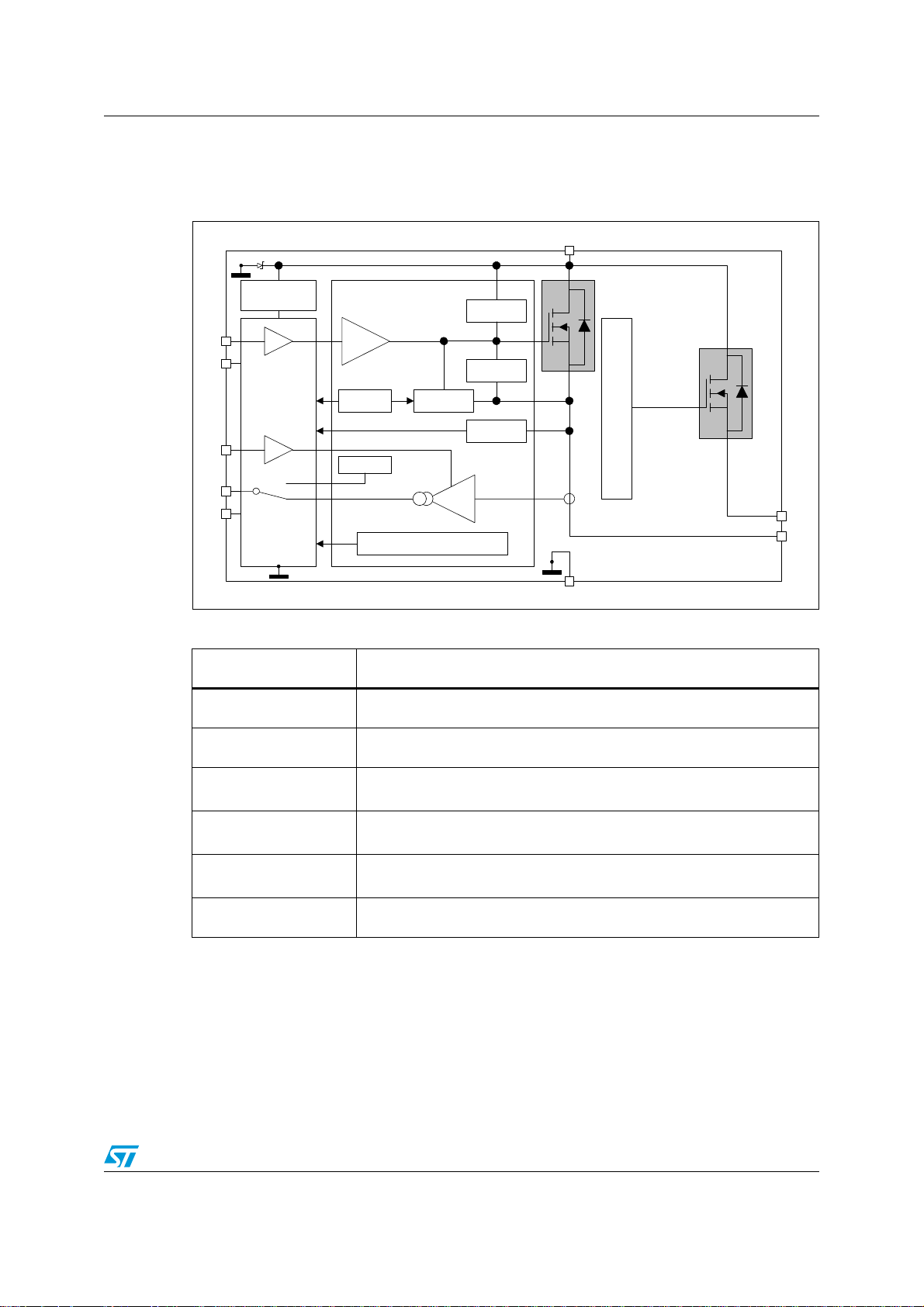
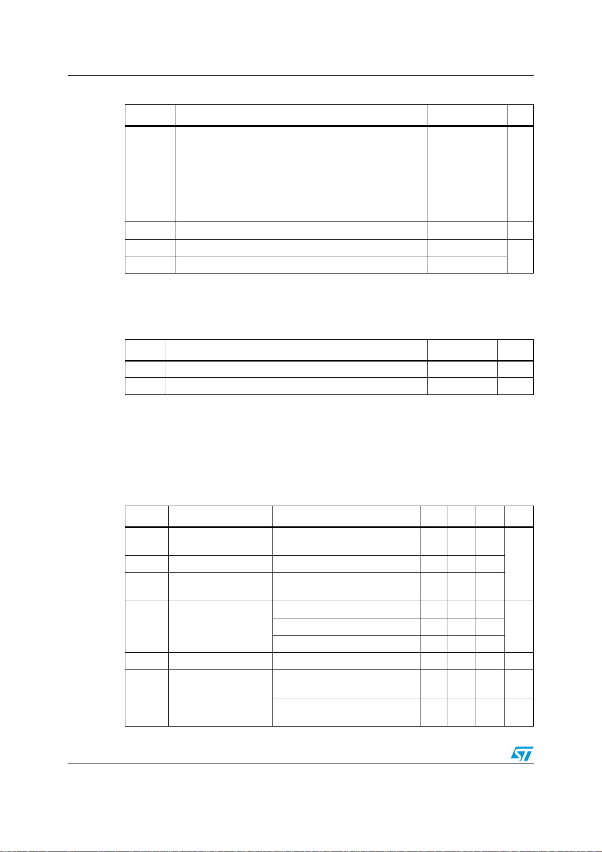
VND5E025AS-E Block diagram and pin description
V
CC
CH 1
Control & Diagnostic 1
LOGIC
DRIVER
V
ON
Limitation
Current
Limitation
Power
Clamp
OFF State
Open load
Over
temp.
Undervoltage
V
SENSEH
Current
Sense
CH 2
OVERLOAD PROTECTION
(ACTIVE POWER LIMITATION)
IN1
IN2
CS1
CS2
CS_
DIS
GND
OUT2
OUT1
Signal Clamp
CONTROL & DIAGNOSTIC
Channels 2
1 Block diagram and pin description
Figure 1. Block diagram
Table 1. Pin functions
OUTPUT
INPUT
CURRENT SENSE
CS_DIS Active high CMOS compatible pin to disable the current sense pin.
Name Function
V
CC
GND
1,2
1,2
Battery connection.
Power output.
Ground connection. Must be reverse battery protected by an external
diode / resistor network.
Voltage controlled input pin with hysteresis, CMOS compatible. It controls
output switch state.
Analog current sense pin; it delivers a current proportional to the load
1,2
current.
Doc ID 022490 Rev 4 5/37
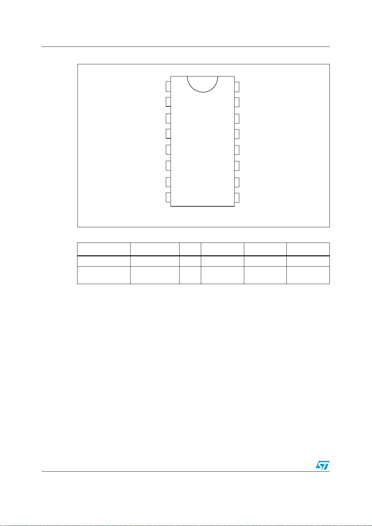
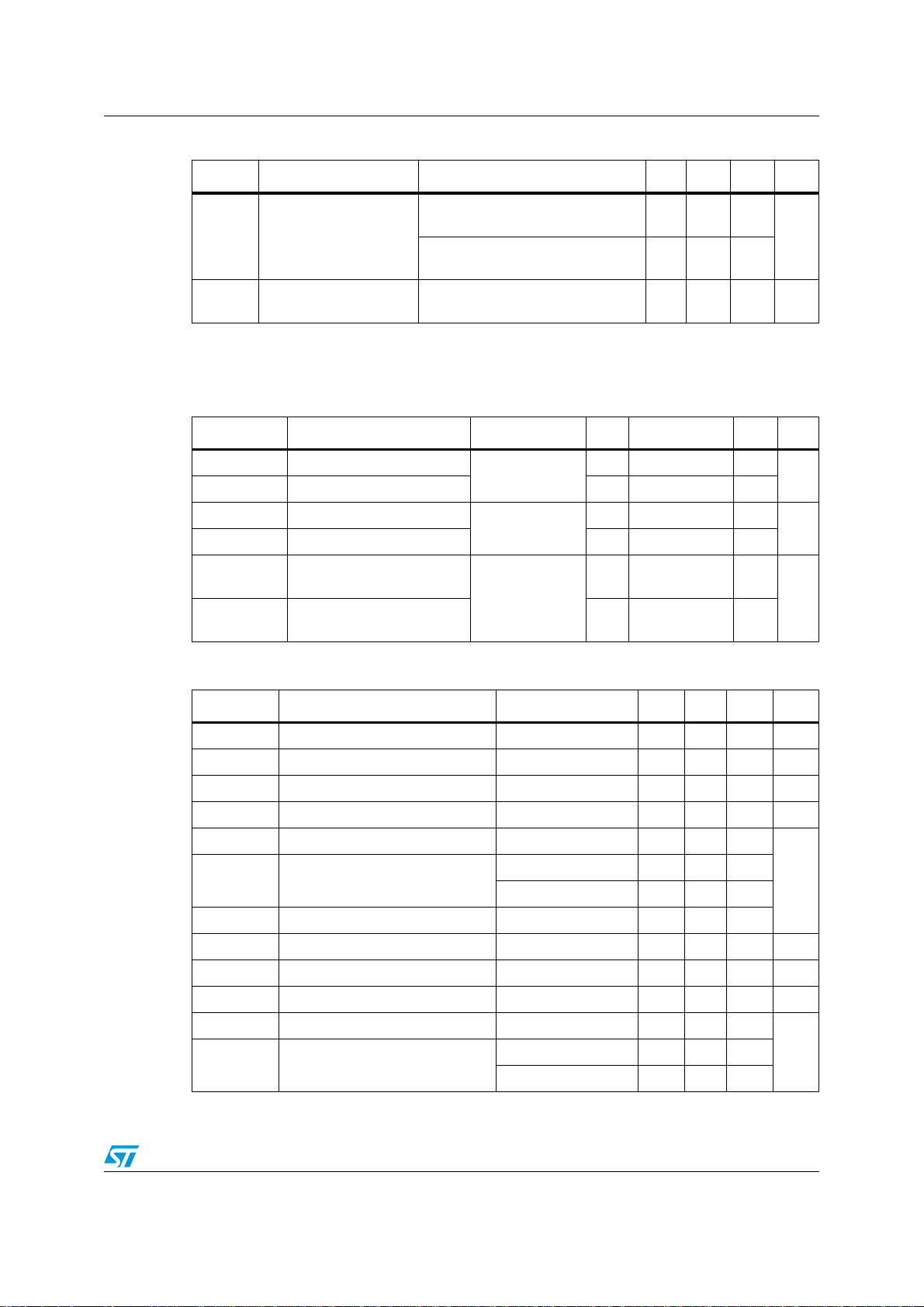
Block diagram and pin description VND5E025AS-E
9FF9FF
9FF9FF
287387
287387
287387
287387
287387
287387
*1'
,1387
,1387
&6(16(
&6(16(
&6',6
("1($'5
Figure 2. Configuration diagram (top view)
Table 2. Suggested connections for unused and not connected pins
Connection / pin Current sense N.C. Output Input CS_DIS
Floating Not allowed X
To ground
1. X: do not care.
Through 1 kΩ
resistor
(1)
Through 22 kΩ
X
XXX
resistor
Through 10 kΩ
resistor
Through 10 kΩ
resistor
6/37 Doc ID 022490 Rev 4
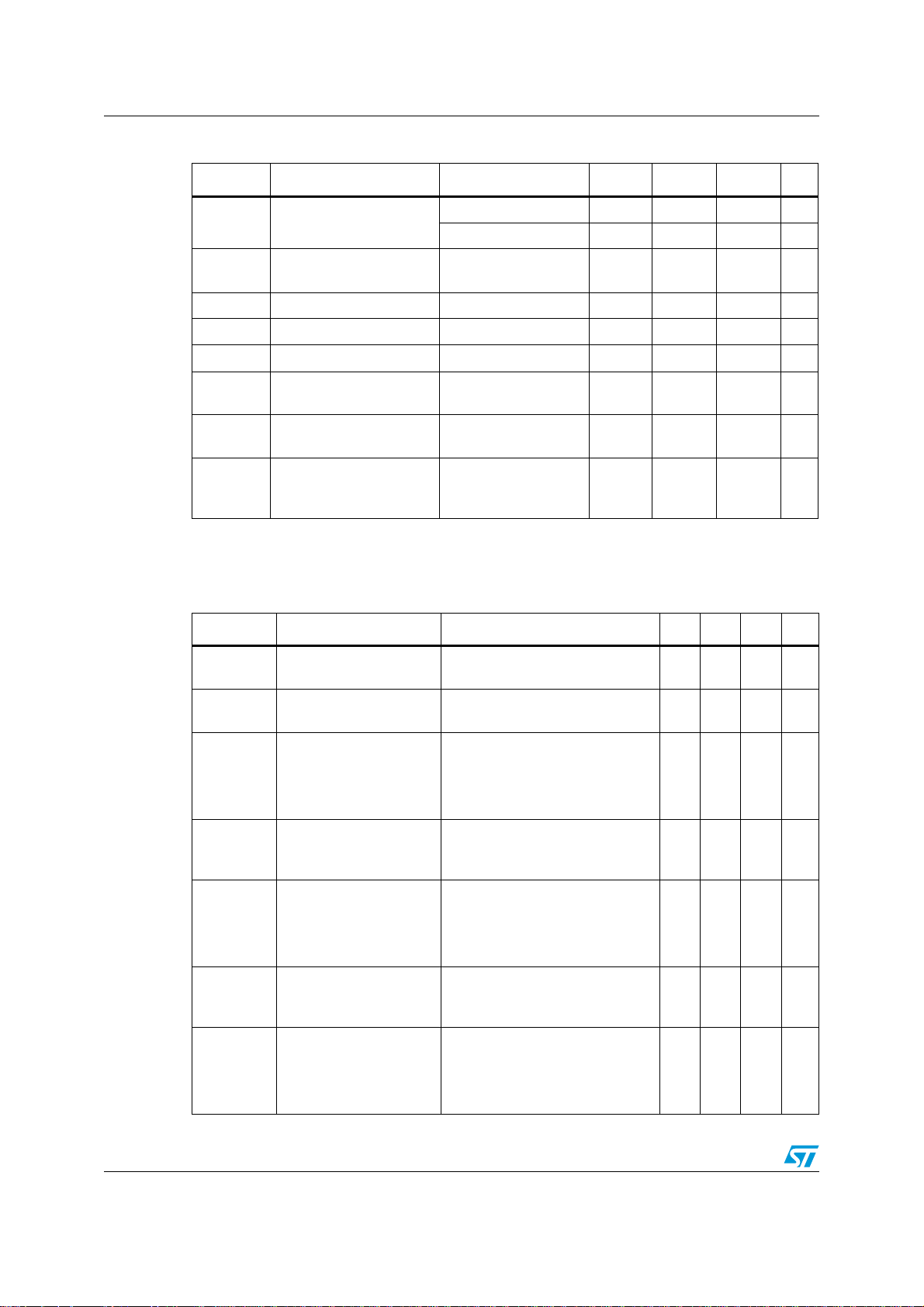
VND5E025AS-E Electrical specifications
V
Fn
I
S
I
GND
V
CC
V
CC
V
SENSE2
OUTPUT1
I
OUT1
CURRENT
I
SENSE1
INPUT1
I
IN1
V
IN2
V
OUT2
GND
CS_DIS
I
CSD
V
CSD
INPUT2
I
IN2
V
IN1
SENSE1
OUTPUT2
I
OUT2
CURRENT
I
SENSE2
SENSE2
V
SENSE1
V
OUT1
2 Electrical specifications
Figure 3. Current and voltage conventions
Note: V
Fn
= V
- VCC during reverse battery condition.
OUTn
2.1 Absolute maximum ratings
Applying stress which exceeds the rating listed in Table 3: Absolute maximum ratings may
cause permanent damage to the device. These are stress ratings only and operation of the
device at these or any other conditions above those indicated in the Operating sections of
this specification is not implied. Exposure to the conditions in table below for extended
periods may affect device reliability.
Table 3. Absolute maximum ratings
Symbol Parameter Value Unit
V
-V
-I
GND
I
OUT
-I
OUT
I
CSD
-I
CSENSE
V
CSENSE
E
MAX
DC supply voltage 41
CC
Reverse DC supply voltage 0.3
CC
DC reverse ground pin current 200 mA
DC output current Internally limited
Reverse DC output current 24
DC input current
IN
-1 to 10
DC current sense disable input current
DC reverse CS pin current 200
Current sense maximum voltage VCC- 41 to +V
Maximum switching energy (single pulse)
(L = 0.8 mH; RL=0Ω; V
I
OUT
= I
limL
(Typ.))
Doc ID 022490 Rev 4 7/37
= 13.5 V; T
bat
jstart
= 150 °C;
V
A
mAI
V
CC
140 mJ
Electrical specifications VND5E025AS-E
Table 3. Absolute maximum ratings (continued)
Symbol Parameter Value Unit
Electrostatic discharge
(Human Body Model: R = 1.5 kΩ; C = 100 pF)
V
V
ESD
ESD
T
– Input
– Current sense
–CS_DIS
– Output
–V
CC
Charge device model (CDM-AEC-Q100-011) 750 V
T
Junction operating temperature -40 to 150
j
Storage temperature -55 to 150
stg
4000
2000
4000
5000
5000
V
V
V
V
V
°C
2.2 Thermal data
Table 4. Thermal data
Symbol Parameter T yp val ue Unit
R
thj-pcb
R
thj-amb
1. The measure is done in accordance with the JESD 51-8.
Thermal resistance junction-pcb
Thermal resistance junction-ambient See Figure 36 °C/W
(1)
18.5 °C/W
2.3 Electrical characteristics
Values specified in this section are for 8 V < VCC< 28 V; -40°C < Tj< 150°C, unless
otherwise stated.
Table 5. Power section
Symbol Parameter Test conditions Min. Typ. Max. Unit
V
V
USDhyst
R
V
clamp
Operating supply
CC
voltage
Undervoltage shutdown 3.5 4.5
USD
Undervoltage shutdown
hysteresis
I
OUT
On-state resistance
ON
(1)
OUT
I
OUT
Clamp voltage IS= 20 mA 41 46 52 V
Off-state; V
V
I
S
Supply current
IN=VOUT=VSENSE=VCSD
On-state; V
I
OUT
4.5 13 28
0.5
=3A; Tj=25°C 25
=3A; Tj=150°C 50
=3A; VCC=5V; Tj=25°C 35
=0A
=13V; Tj=25°C;
CC
=13V; VIN=5V;
CC
=0V
(2)5(2)
2
36mA
VV
mΩI
µA
8/37 Doc ID 022490 Rev 4
VND5E025AS-E Electrical specifications
Table 5. Power section (continued)
Symbol Parameter Test conditions Min. Typ. Max. Unit
VIN=V
= 25°C
T
I
L(off1)
1. For each channel.
2. PowerMOS leakage included.
Table 6. Switching (VCC=13V; Tj= 25°C)
Off-state output
current
Output - VCC diode
V
F
voltage
(1)
(1)
j
V
IN=VOUT
= 125°C
T
j
-I
OUT
=0V; VCC=13V;
OUT
=0V; VCC=13V;
00.013
05
=4 A; Tj= 150°C 0.7 V
Symbol Parameter Test conditions Min. Typ. Max. Unit
t
d(on)
t
d(off)
(dV
/dt)onTurn-on voltage slope
OUT
/dt)
(dV
OUT
W
ON
W
OFF
Tu r n - o n d e l a y t i m e
Turn-off delay time — 40 —
Turn-off voltage slope — See Figure 28 —
off
Switching energy losses
during t
Switching energy losses
during t
WON
WOFF
R
=4.3 Ω
L
(see Figure 6)
=4.3 Ω
R
L
RL=4.3 Ω
(see Figure 6)
—20—
—See Figure 27 —
—0.6—
—0.35—
µA
µs
V/µs
mJ
Table 7. Logic inputs
Symbol Parameter Test conditions Min. Typ. Max. Unit
V
IL
I
IL
V
IH
I
IH
V
I(hyst)
ICL
V
CSDL
I
CSDL
V
CSDH
I
CSDH
V
CSD(hyst)
V
CSCL
Input low level voltage 0.9 V
Low level input current VIN=0.9V 1 µA
Input high level voltage 2.1 V
High level input current VIN=2.1V 10 µA
Input hysteresis voltage 0.25
I
=1mA 5.5 7
Input clamp voltage
IN
I
=-1mA -0.7
IN
CS_DIS low level voltage 0.9
Low level CS_DIS current V
=0.9V 1 µA
CSD
CS_DIS high level voltage 2.1 V
High level CS_DIS current V
=2.1V 10 µA
CSD
CS_DIS hysteresis voltage 0.25
=1mA 5.5 7
I
CS_DIS clamp voltage
CSD
I
=-1mA -0.7
CSD
VV
V
Doc ID 022490 Rev 4 9/37
Electrical specifications VND5E025AS-E
Table 8. Protections and diagnostics
(1)
Symbol Parameter Test conditions Min. Typ. Max. Unit
= 13 V 43 60 85 A
V
I
LIMH
I
LIML
T
TSD
T
T
RS
T
HYST
V
DEMAG
V
ON
1. To ensure long term reliability under heavy overload or short circuit conditions, protection and related
diagnostic signals must be used together with a proper software strategy. If the device is subjected to
abnormal conditions, this software must limit the duration and number of activation cycles.
T able 9. Current sense (8 V < VCC<18V)
DC short circuit current
Short circuit current
during thermal cycling
Shutdown temperature 150 175 200 °C
Reset temperature TRS+1 TRS+5 °C
R
Thermal reset of STATUS 135 °C
Thermal hysteresis
TSD-TR
)
(T
Turn-Off output voltage
clamp
Output voltage drop
limitation
CC
5V<VCC<28V 85 A
VCC=13V;
T
R<Tj<TTSD
15 A
7°C
I
=2A; VIN=0;
OUT
L=6 mH
=0.1A;
I
OUT
= -40°C to 150°C
T
j
VCC-41 VCC-46 VCC-52 V
25 mV
(see Figure 8)
Symbol Parameter Test conditions Min. Typ. Max. Unit
I
dK
dK
K
LED
K
K
1/K1
K
2/K2
K
= 0.05 A; V
I
OUT/ISENSE
0
1
2
3
I
OUT/ISENSE
I
OUT/ISENSE
(1)
Current sense ratio drift
I
OUT/ISENSE
(1)
Current sense ratio drift
I
OUT/ISENSE
OUT
V
=0V; Tj= -40°C to 150°C
CSD
I
= 0.5 A; V
OUT
=0V; Tj= -40 °C to 150 °C
V
CSD
I
=2 A; V
OUT
V
=0V;
CSD
T
= -40°C to 150°C
j
T
= 25°C to 150°C
j
I
=2 A; V
OUT
=0V;
V
CSD
T
= -40°C to 150°C
j
I
=3 A; V
OUT
=0V;
V
CSD
SENSE
SENSE
SENSE
SENSE
Tj= -40°C to 150°C
T
= 25°C to150°C
j
=3 A; V
I
OUT
V
CSD
= -40°C to 150°C
T
j
I
= 10 A; V
OUT
V
CSD
SENSE
=0V;
SENSE
=0V;
Tj= -40°C to 150°C
Tj= 25°C to 150°C
SENSE
=4 V;
=4 V;
=4V;
=4V;
=0.5V;
=0.5V;
=4V;
1240 3350 5100
1860 3150 4600
2100
3100
4400
2250
3100
3850
-13 13 %
2200
3000
4100
2450
3000
3550
-12 12 %
2550
2850
3280
2650
2850
3180
10/37 Doc ID 022490 Rev 4
VND5E025AS-E Electrical specifications
T able 9. Current sense (8 V < VCC< 18 V) (continued)
Symbol Parameter Test conditions Min. Typ. Max. Unit
dK3/K
I
SENSE
I
OL
V
SENSE
V
SENSEH
I
SENSEH
(1)
Current sense ratio drift
3
Analog sense leakage
0
current
Open-load on-state
current detection
threshold
Max analog sense output
voltage
Analog sense output
voltage in fault
condition
(1)
Analog sense output
current in fault
condition
(2)
= 10 A; V
I
OUT
=0V; Tj= -40°C to 150°C
V
CSD
=0A; V
I
OUT
=5V; VIN=0V;
V
CSD
= -40°C to 150°C
T
j
I
=0A; V
OUT
=0V; VIN=5V;
V
CSD
= -40 °C to 150 °C
T
j
I
=2A; V
OUT
=5V; VIN=5V;
V
CSD
= -40°C to 150°C
T
j
= 5V; 8V<VCC<18V;
V
IN
I
SENSE
=3 A; V
I
OUT
VCC=13V; R
VCC=13V; V
= 5 µA
SENSE
=0V;
SENSE
=0V;
SENSE
=0V;
SENSE
=0V 5 V
CSD
SENSE
SENSE
=4V;
-6 +6 %
01µA
02µA
01µA
530mA
=3.9kΩ 8V
=5V 9 mA
Delay response time
t
DSENSE1H
from falling edge of
CS_DIS pin
Delay response time
t
DSENSE1L
from rising edge of
CS_DIS pin
Delay response time
t
DSENSE2H
from rising edge of
INPUT pin
Delay response time
Δt
DSENSE2H
between rising edge of
output current and rising
edge of current sense
Delay response time
t
DSENSE2L
from falling edge of
INPUT pin
1. Fault condition includes: power limitation, overtemperature and open-load off-state detection.
V
I
SENSE
SENSE
<4V, 0.5<I
= 90% of I
(see Figure 4)
V
I
SENSE
SENSE
<4V, 0.5<I
=10% of I
(see Figure 4)
V
I
SENSE
SENSE
<4V, 0.5<I
= 90% of I
(see Figure 4)
V
I
SENSE
I
OUT
I
OUTMAX
V
I
SENSE
SENSE
=90% of I
=90% of I
SENSE
<4V,
=3A; (see Figure 7)
<4V, 0.5<I
=10% of I
(see Figure 4)
OUT
SENSEMAX
OUT
SENSEMAX
OUT
SENSEMAX
SENSEMAX,
OUTMAX
OUT
SENSEMAX
<10A
<10A
<10A
;
<10A
30 100 µs
520µs
80 300 µs
110 µs
70 250 µs
Doc ID 022490 Rev 4 11/37
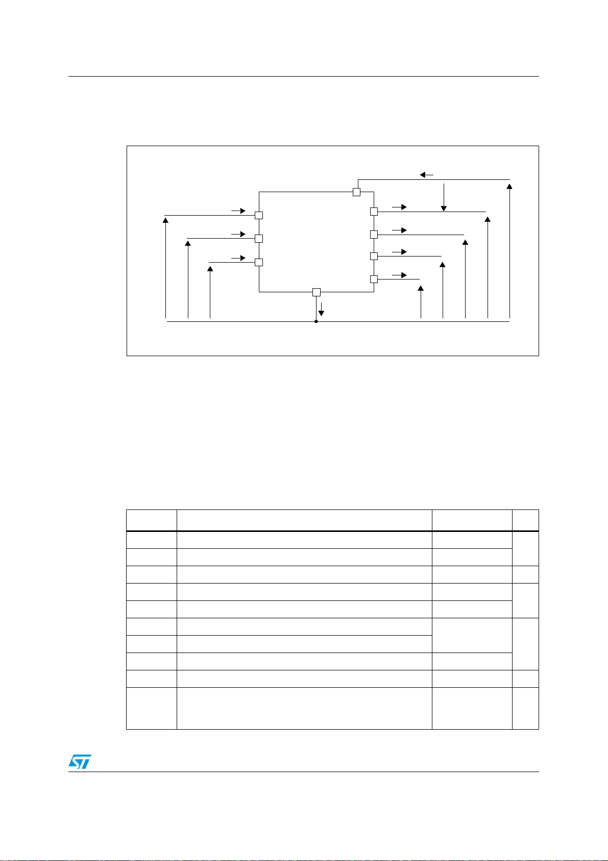
Electrical specifications VND5E025AS-E
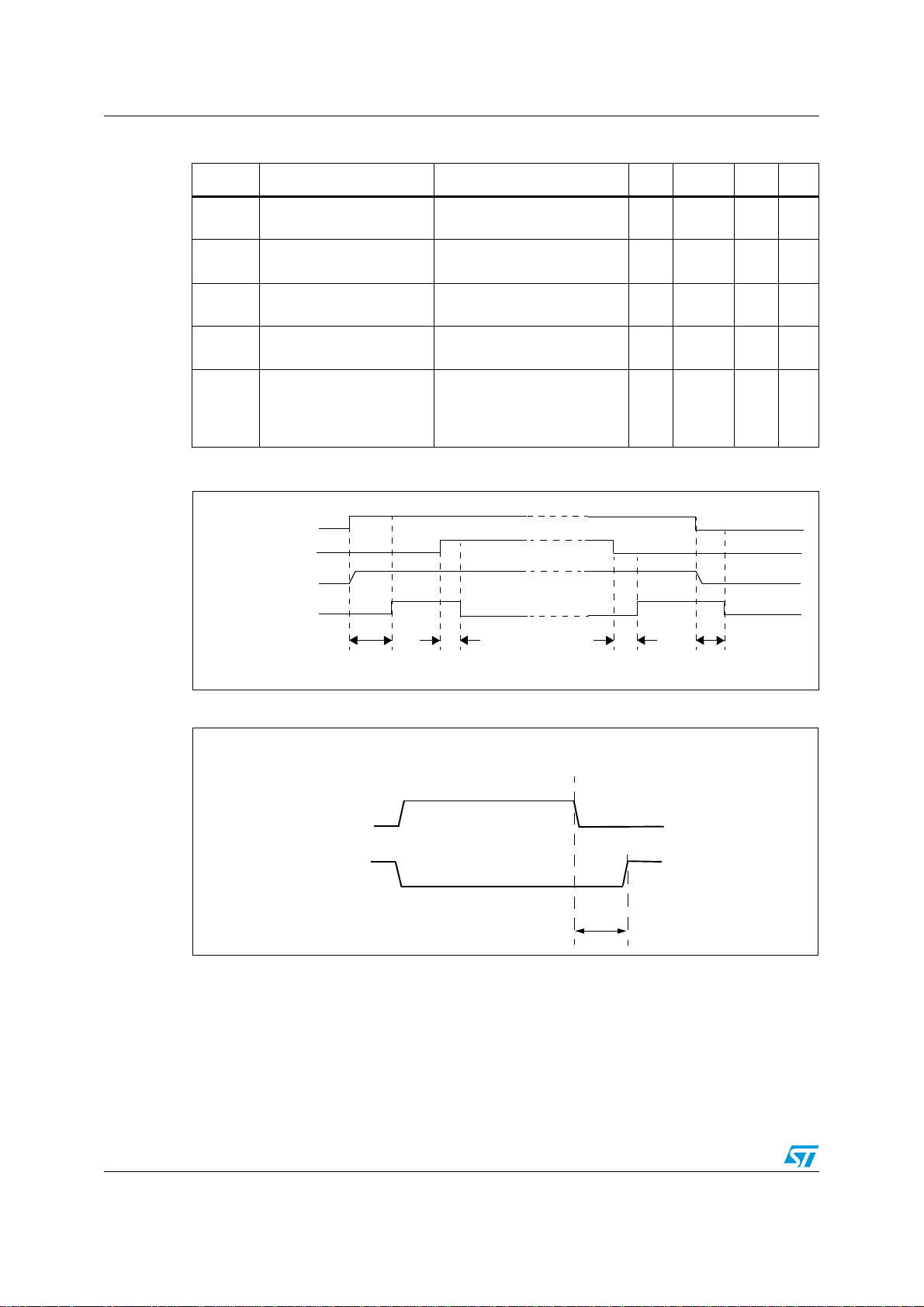
SENSE CURRENT
INPUT
LOAD CURRENT
CS_DIS
t
DSENSE2H
t
DSENSE2L
t
DSENSE1L
t
DSENSE1H
V
IN
V
CS
t
DSTKON
OUTPUT STUCK TO V
CC
V
OUT
> V
OL
V
SENSEH
Table 10. Open-load detection (8 V < V
Symbol Parameter Test condition Min. Typ. Max. Unit
CC
<18V)
V
t
DSTKON
I
L(off2)r
I
L(off2)f
Open-load off-state
OL
voltage detection threshold
Output short circuit to V
detection delay at turn-off
Off-state output current at
= 4V
V
OUT
Off-state output current at
V
= 2 V
OUT
VIN=0V 2
CC
See Figure 5 180 1200 µs
V
=0V; V
V
V
V
IN
OUT
IN
OUT
=0V; V
SENSE
rising from 0 V to 4 V
SENSE=VSENSEH
falling from VCC to 2 V
Delay response from
td_vol
output rising edge to
V
SENSE
rising edge in
= 4 V; VIN= 0 V;
V
OUT
V
SENSE
= 90 % of V
openload
Figure 4. Current sense delay characteristics
=0V;
SENSEH
See
Figure 5
4V
-120 0 µA
;
-50 90 µA
20 µs
12/37 Doc ID 022490 Rev 4
Figure 5. Open-load off-state delay timing
 Loading...