

Features
VND5E004A-E
VND5E004ASP30-E
Double 4mΩ high-side driver with analog current sense
for automotive applications
Max transient supply voltage V
Operating voltage range V
Max on-state resistance (per ch.) R
Current limitation (typ) I
Off-state supply current I
1. Typical value with all loads connected
■ General
CC
CC
ON
LIMH
S
4.5 to 28 V
– Very low standby current
– 3.0 V CMOS compatible inputs
– Optimized electromagnetic emissions
– Very low electromagnetic susceptibility
– Compliant with European directive
2002/95/EC
– Very low current sense leakage
■ Diagnostic functions
– Proportional load current sense
– High current sense precision for wide
currents range
– Diagnostic enable pin
– Off-state open-load detection
– Output short to V
detection
CC
– Overload and short to ground (power
limitation) indication
– Thermal shutdown indication
■ Protection
– Undervoltage shutdown
– Overvoltage clamp
– Load current limitation
– Self limiting of fast thermal transients
– Protection against loss of ground and loss
of V
CC
– Overtemperature shutdown with auto
restart (thermal shutdown)
– Inrush current active management by
power limitation
41 V
4mΩ
90 A
2µA
(1)
MultiPowerSO-30PQFN - 12x12 Power lead-less
– Reverse battery protection with self switch
on of the Power MOSFET
– Electrostatic discharge protection
Applications
■ All types of resistive, inductive and capacitive
loads
■ Suitable for power management applications
Description
The VND5E004A-E and VND5E004ASP30-E are
double channel high-side drivers manufactured
using ST proprietary VIPower™ M0-5 technology
and housed in PQFN-12x12 power lead-less and
MultiPowerSO-30 packages. The devices are
designed to drive 12 V automotive grounded
loads, and to provide protection and diagnostics.
They also implement a 3 V and 5 V CMOScompatible interface for use with any
microcontroller.
The devices integrate advanced protective
functions such as load current limitation, inrush
and overload active management by power
limitation, overtemperature shut-off with autorestart and overvoltage active clamp. A dedicated
analog current sense pin is associated with every
output channel providing enhanced diagnostic
functions including fast detection of overload and
short-circuit to ground through power limitation
indication, overtemperature indication, shortcircuit to V
open-load detection. The current sensing and
diagnostic feedback of the whole device can be
disabled by pulling the DE pin low to share the
external sense resistor with similar devices.
diagnosis and on-state and off-state
CC
July 2010 Doc ID 17359 Rev 1 1/45
www.st.com
1

Contents VND5E004A-E / VND5E004ASP30-E
Contents
1 Block diagram and pin configurations . . . . . . . . . . . . . . . . . . . . . . . . . . 6
2 Electrical specifications . . . . . . . . . . . . . . . . . . . . . . . . . . . . . . . . . . . . . . 8
2.1 Absolute maximum ratings . . . . . . . . . . . . . . . . . . . . . . . . . . . . . . . . . . . . . 8
2.2 Thermal data . . . . . . . . . . . . . . . . . . . . . . . . . . . . . . . . . . . . . . . . . . . . . . . 9
2.3 Electrical characteristics . . . . . . . . . . . . . . . . . . . . . . . . . . . . . . . . . . . . . . 10
2.4 Waveforms . . . . . . . . . . . . . . . . . . . . . . . . . . . . . . . . . . . . . . . . . . . . . . . . 19
2.5 Electrical characteristics curves . . . . . . . . . . . . . . . . . . . . . . . . . . . . . . . . 22
3 Application information . . . . . . . . . . . . . . . . . . . . . . . . . . . . . . . . . . . . . 25
3.1 MCU I/Os protection . . . . . . . . . . . . . . . . . . . . . . . . . . . . . . . . . . . . . . . . . 25
3.2 Load dump protection . . . . . . . . . . . . . . . . . . . . . . . . . . . . . . . . . . . . . . . . 25
3.3 Current sense and diagnostic . . . . . . . . . . . . . . . . . . . . . . . . . . . . . . . . . . 26
3.3.1 Short to VCC and off-state open-load detection . . . . . . . . . . . . . . . . . . 27
3.4 Maximum demagnetization energy (VCC = 13.5V) . . . . . . . . . . . . . . . . . 29
4 Package and PC board thermal data . . . . . . . . . . . . . . . . . . . . . . . . . . . 30
4.1 MultiPowerSO-30 thermal data . . . . . . . . . . . . . . . . . . . . . . . . . . . . . . . . 30
4.2 PQFN - 12x12 power lead-less thermal data . . . . . . . . . . . . . . . . . . . . . . 33
5 Package and packing information . . . . . . . . . . . . . . . . . . . . . . . . . . . . . 36
5.1 ECOPACK® packages . . . . . . . . . . . . . . . . . . . . . . . . . . . . . . . . . . . . . . . 36
5.2 MultiPowerSO-30 mechanical data . . . . . . . . . . . . . . . . . . . . . . . . . . . . . 36
5.3 PQFN - 12x12 power lead-less mechanical data . . . . . . . . . . . . . . . . . . . 38
5.4 MultiPowerSO-30 packing information . . . . . . . . . . . . . . . . . . . . . . . . . . . 40
5.5 PQFN - 12x12 power lead-less packing information . . . . . . . . . . . . . . . . 41
6 Order codes . . . . . . . . . . . . . . . . . . . . . . . . . . . . . . . . . . . . . . . . . . . . . . . 43
7 Revision history . . . . . . . . . . . . . . . . . . . . . . . . . . . . . . . . . . . . . . . . . . . 44
2/45 Doc ID 17359 Rev 1

VND5E004A-E / VND5E004ASP30-E List of tables
List of tables
Table 1. Pin functions . . . . . . . . . . . . . . . . . . . . . . . . . . . . . . . . . . . . . . . . . . . . . . . . . . . . . . . . . . . . . 6
Table 2. Suggested connections for unused and not connected pins . . . . . . . . . . . . . . . . . . . . . . . . 7
Table 3. Absolute maximum ratings . . . . . . . . . . . . . . . . . . . . . . . . . . . . . . . . . . . . . . . . . . . . . . . . . . 8
Table 4. Thermal data. . . . . . . . . . . . . . . . . . . . . . . . . . . . . . . . . . . . . . . . . . . . . . . . . . . . . . . . . . . . . 9
Table 5. Power section . . . . . . . . . . . . . . . . . . . . . . . . . . . . . . . . . . . . . . . . . . . . . . . . . . . . . . . . . . . 10
Table 6. Switching (VCC = 13 V; Tj = 25 °C) . . . . . . . . . . . . . . . . . . . . . . . . . . . . . . . . . . . . . . . . . . 11
Table 7. Logic inputs. . . . . . . . . . . . . . . . . . . . . . . . . . . . . . . . . . . . . . . . . . . . . . . . . . . . . . . . . . . . . 11
Table 8. Protections and diagnostics . . . . . . . . . . . . . . . . . . . . . . . . . . . . . . . . . . . . . . . . . . . . . . . . 12
Table 9. Current sense (8 V < V
Table 10. Open-load detection (8V<V
Table 11. Truth table. . . . . . . . . . . . . . . . . . . . . . . . . . . . . . . . . . . . . . . . . . . . . . . . . . . . . . . . . . . . . . 17
Table 12. Electrical transient requirements (part 1/3) . . . . . . . . . . . . . . . . . . . . . . . . . . . . . . . . . . . . . 18
Table 13. Electrical transient requirements (part 2/3) . . . . . . . . . . . . . . . . . . . . . . . . . . . . . . . . . . . . . 18
Table 14. Electrical transient requirements (part 3/3) . . . . . . . . . . . . . . . . . . . . . . . . . . . . . . . . . . . . . 18
Table 15. Thermal parameters for MultiPowerSO-30 . . . . . . . . . . . . . . . . . . . . . . . . . . . . . . . . . . . . . 32
Table 16. Thermal parameters for PQFN - 12x12 power lead-less . . . . . . . . . . . . . . . . . . . . . . . . . . 35
Table 17. MultiPowerSO-30 mechanical data . . . . . . . . . . . . . . . . . . . . . . . . . . . . . . . . . . . . . . . . . . 37
Table 18. PQFN - 12x12 power lead-less mechanical data . . . . . . . . . . . . . . . . . . . . . . . . . . . . . . . . 39
Table 19. Device summary . . . . . . . . . . . . . . . . . . . . . . . . . . . . . . . . . . . . . . . . . . . . . . . . . . . . . . . . . 43
Table 20. Document revision history . . . . . . . . . . . . . . . . . . . . . . . . . . . . . . . . . . . . . . . . . . . . . . . . . 44
< 18 V) . . . . . . . . . . . . . . . . . . . . . . . . . . . . . . . . . . . . . . . . . . . 12
CC
<18V, VDE= 5V) . . . . . . . . . . . . . . . . . . . . . . . . . . . . . . . . . 14
CC
Doc ID 17359 Rev 1 3/45

List of figures VND5E004A-E / VND5E004ASP30-E
List of figures
Figure 1. Block diagram . . . . . . . . . . . . . . . . . . . . . . . . . . . . . . . . . . . . . . . . . . . . . . . . . . . . . . . . . . . . 6
Figure 2. Configuration diagram (not in scale). . . . . . . . . . . . . . . . . . . . . . . . . . . . . . . . . . . . . . . . . . . 7
Figure 3. Current and voltage conventions . . . . . . . . . . . . . . . . . . . . . . . . . . . . . . . . . . . . . . . . . . . . . 8
Figure 4. Current sense delay characteristics . . . . . . . . . . . . . . . . . . . . . . . . . . . . . . . . . . . . . . . . . . 14
Figure 5. Open-load off-state delay timing. . . . . . . . . . . . . . . . . . . . . . . . . . . . . . . . . . . . . . . . . . . . . 14
Figure 6. Switching characteristics . . . . . . . . . . . . . . . . . . . . . . . . . . . . . . . . . . . . . . . . . . . . . . . . . . 15
Figure 7. Delay response time between rising edge of output current and rising edge of current sense
(CS enabled) . . . . . . . . . . . . . . . . . . . . . . . . . . . . . . . . . . . . . . . . . . . . . . . . . . . . . . . . . . . 15
Figure 8. Output voltage drop limitation . . . . . . . . . . . . . . . . . . . . . . . . . . . . . . . . . . . . . . . . . . . . . . . 16
Figure 9. I
OUT/ISENSE
Figure 10. Maximum current sense ratio drift vs load current
Figure 11. Normal operation . . . . . . . . . . . . . . . . . . . . . . . . . . . . . . . . . . . . . . . . . . . . . . . . . . . . . . . . 19
Figure 12. Overload or short to GND . . . . . . . . . . . . . . . . . . . . . . . . . . . . . . . . . . . . . . . . . . . . . . . . . . 19
Figure 13. Intermittent overload . . . . . . . . . . . . . . . . . . . . . . . . . . . . . . . . . . . . . . . . . . . . . . . . . . . . . . 20
Figure 14. Off-state open-load with external circuitry . . . . . . . . . . . . . . . . . . . . . . . . . . . . . . . . . . . . . 20
Figure 15. Short to V
Figure 16. T
evolution in overload or short to GND . . . . . . . . . . . . . . . . . . . . . . . . . . . . . . . . . . . . . . 21
J
Figure 17. Off-state output current. . . . . . . . . . . . . . . . . . . . . . . . . . . . . . . . . . . . . . . . . . . . . . . . . . . . 22
Figure 18. High level input current . . . . . . . . . . . . . . . . . . . . . . . . . . . . . . . . . . . . . . . . . . . . . . . . . . . . 22
Figure 19. Input clamp voltage. . . . . . . . . . . . . . . . . . . . . . . . . . . . . . . . . . . . . . . . . . . . . . . . . . . . . . . 22
Figure 20. Input low level voltage . . . . . . . . . . . . . . . . . . . . . . . . . . . . . . . . . . . . . . . . . . . . . . . . . . . . 22
Figure 21. Input high level voltage . . . . . . . . . . . . . . . . . . . . . . . . . . . . . . . . . . . . . . . . . . . . . . . . . . . . 22
Figure 22. Input hysteresis voltage . . . . . . . . . . . . . . . . . . . . . . . . . . . . . . . . . . . . . . . . . . . . . . . . . . . 22
Figure 23. On-state resistance vs T
Figure 24. On-state resistance vs V
Figure 25. Undervoltage shutdown . . . . . . . . . . . . . . . . . . . . . . . . . . . . . . . . . . . . . . . . . . . . . . . . . . . 23
Figure 26. Turn-on voltage slope . . . . . . . . . . . . . . . . . . . . . . . . . . . . . . . . . . . . . . . . . . . . . . . . . . . . . 23
Figure 27. I
LIMH
vs T
Figure 28. Turn-off voltage slope . . . . . . . . . . . . . . . . . . . . . . . . . . . . . . . . . . . . . . . . . . . . . . . . . . . . . 23
Figure 29. DE high level voltage . . . . . . . . . . . . . . . . . . . . . . . . . . . . . . . . . . . . . . . . . . . . . . . . . . . . . 24
Figure 30. DE clamp voltage . . . . . . . . . . . . . . . . . . . . . . . . . . . . . . . . . . . . . . . . . . . . . . . . . . . . . . . . 24
Figure 31. DE low level voltage . . . . . . . . . . . . . . . . . . . . . . . . . . . . . . . . . . . . . . . . . . . . . . . . . . . . . . 24
Figure 32. Application schematic . . . . . . . . . . . . . . . . . . . . . . . . . . . . . . . . . . . . . . . . . . . . . . . . . . . . 25
Figure 33. Current sense and diagnostics . . . . . . . . . . . . . . . . . . . . . . . . . . . . . . . . . . . . . . . . . . . . . 27
Figure 34. Maximum turn-off current versus inductance
Figure 35. MultiPowerSO-30 PC board
Figure 36. Rthj-amb vs PCB copper area in open box free air condition (one channel ON) . . . . . . . . 30
Figure 37. MultiPowerSO-30 thermal impedance junction ambient single pulse (one channel ON) . . 31
Figure 38. Thermal fitting model of a double channel HSD in MultiPowerSO-30
Figure 39. 12x12 Power lead-less package PC board
Figure 40. Rthj-amb vs PCB copper area in open box free air condition (one channel ON) . . . . . . . . 33
Figure 41. PQFN - 12x12 power lead-less package thermal impedance junction ambient single pulse
(one channel ON) . . . . . . . . . . . . . . . . . . . . . . . . . . . . . . . . . . . . . . . . . . . . . . . . . . . . . . . . 34
Figure 42. Thermal fitting model of a double channel HSD in PQFN - 12x12 power lead-less
Figure 43. MultiPowerSO-30 outline . . . . . . . . . . . . . . . . . . . . . . . . . . . . . . . . . . . . . . . . . . . . . . . . . . 36
Figure 44. PQFN - 12x12 power lead-less outline . . . . . . . . . . . . . . . . . . . . . . . . . . . . . . . . . . . . . . . . 38
Figure 45. MultiPowerSO-30 tube shipment (no suffix) . . . . . . . . . . . . . . . . . . . . . . . . . . . . . . . . . . . 40
Figure 46. MultiPowerSO-30 tape and reel shipment (suffix “TR”) . . . . . . . . . . . . . . . . . . . . . . . . . . . 40
vs I
. . . . . . . . . . . . . . . . . . . . . . . . . . . . . . . . . . . . . . . . . . . . . . . . . . . . . . . . . . . . 21
CC
case
. . . . . . . . . . . . . . . . . . . . . . . . . . . . . . . . . . . . . . . . . . . . . . . . . . . . . . 16
OUT
. . . . . . . . . . . . . . . . . . . . . . . . . . . . . . . . . . . . . . . . . . . . . . . . 23
case
. . . . . . . . . . . . . . . . . . . . . . . . . . . . . . . . . . . . . . . . . . . . . . . . . 23
CC
(1)
. . . . . . . . . . . . . . . . . . . . . . . . . . . . . 17
. . . . . . . . . . . . . . . . . . . . . . . . . . . . . . . . . . . . . . . . . . . . . . . . . . . . . . . . . . . 23
(1)
(1)
. . . . . . . . . . . . . . . . . . . . . . . . . . . . . . . . . . . . . . . . . . . . . . 30
. . . . . . . . . . . . . . . . . . . . . . . . . . . . . . . . . 29
(1)
(1)
. . . . . . . . . . . . . . . . . . . . . . . . . . . . . . . . . . . 33
. . . . . . . . . . . . . . 31
(1)
. . . . 34
4/45 Doc ID 17359 Rev 1

VND5E004A-E / VND5E004ASP30-E List of figures
Figure 47. PQFN - 12x12 power lead-less tray shipment (no suffix) . . . . . . . . . . . . . . . . . . . . . . . . . . 41
Figure 48. PQFN - 12x12 power lead-less tape and reel shipment (suffix “TR”) . . . . . . . . . . . . . . . . . 42
Doc ID 17359 Rev 1 5/45
Block diagram and pin configurations VND5E004A-E / VND5E004ASP30-E
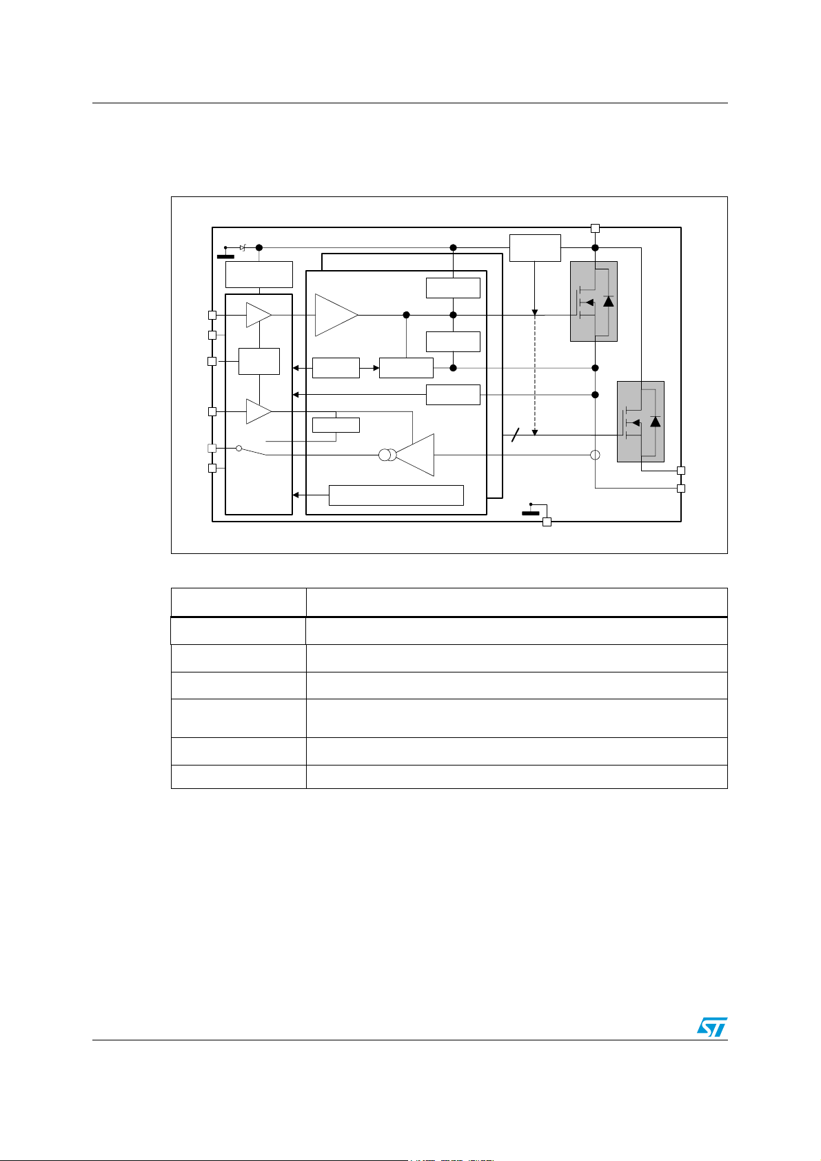
1 Block diagram and pin configurations
Figure 1. Block diagram
V
CC
Reverse
Battery
Protection
CH 1
CH 2
OUT2
OUT1
IN1
IN2
CE
CS_
DIS
CS1
CS2
Signal Clamp
Undervoltage
Device
Enable
LOGIC
Control & Diagnostic 2
Control & Diagnostic 1
DRIVER
Over
temp.
V
SENSEH
OVERLOAD P ROTECTION
(ACTIVE POWER LIMITATION)
Current
Limitation
Current
Sense
Power
Clamp
V
ON
Limitation
OFF State
Open load
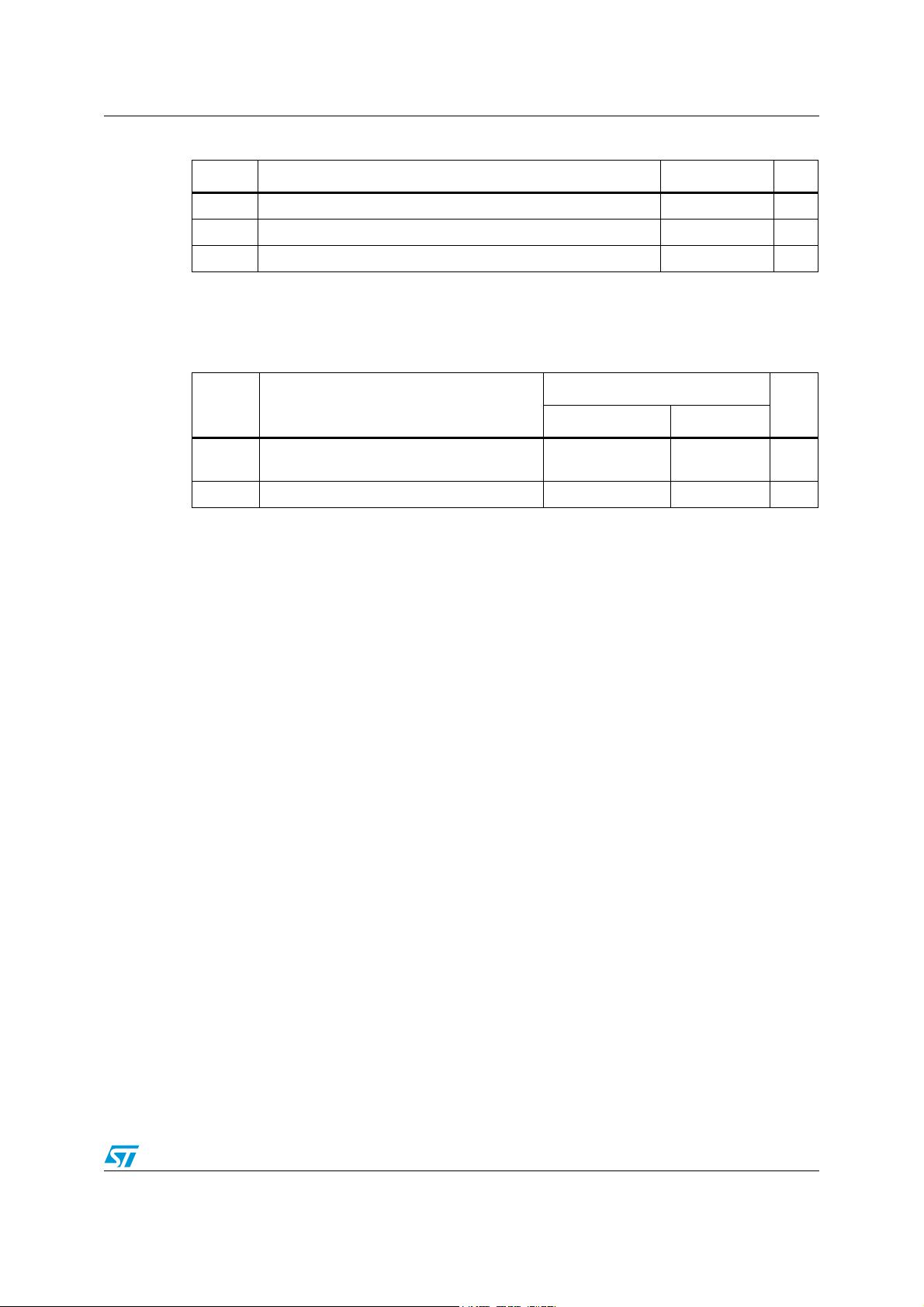
Table 1. Pin functions
Name Function
V
CC
Battery connection
OUT1,2 Power output
GND Ground connection
IN1,2
Voltage controlled input pin with hysteresis, CMOS compatible, controls
output switch state
CS1,2 Analog current sense pin; delivers a current proportional to the load current
DE Active high diagnostic enable pin
GND
6/45 Doc ID 17359 Rev 1
VND5E004A-E / VND5E004ASP30-E Block diagram and pin configurations
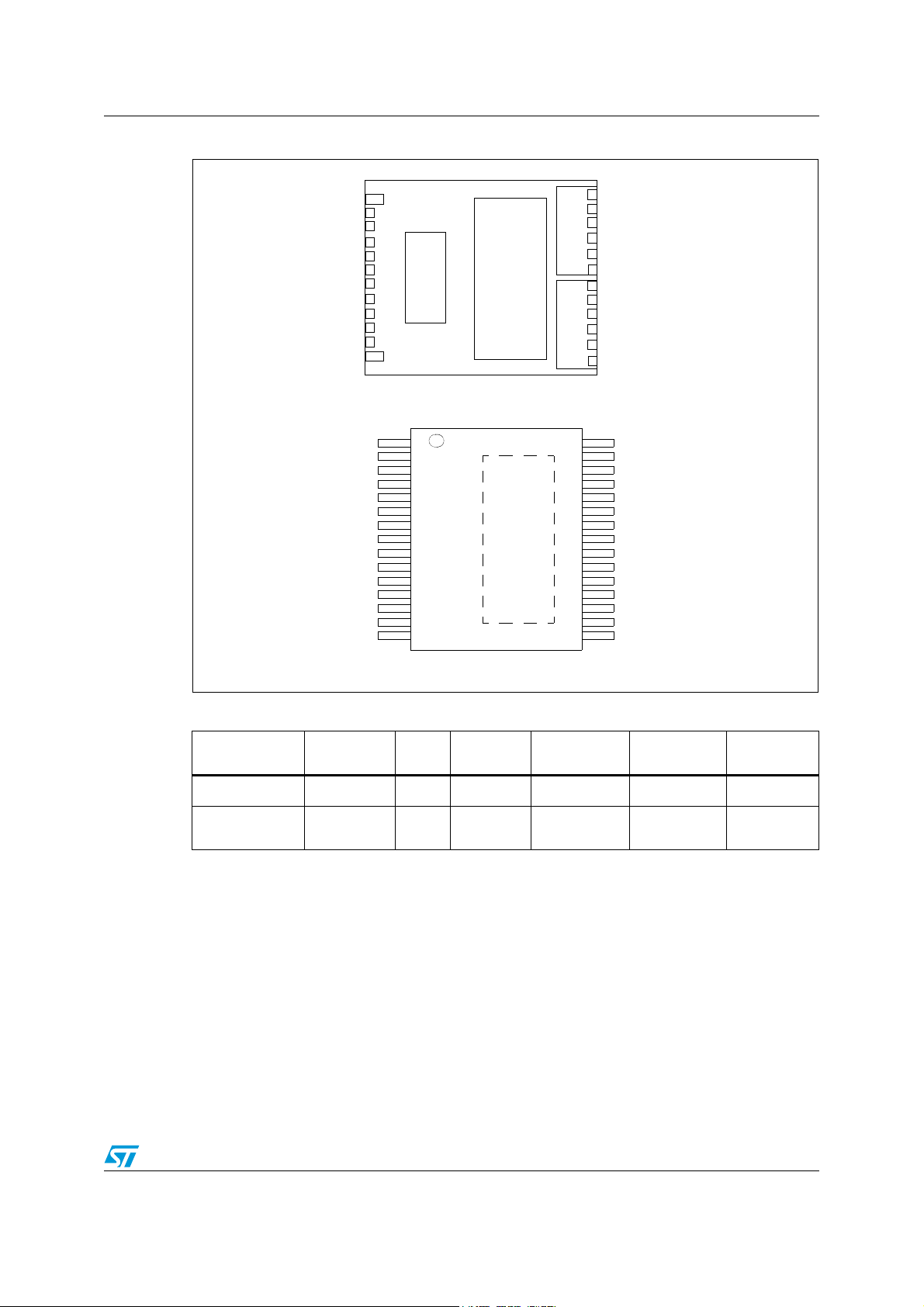
Figure 2. Configuration diagram (not in scale)
1 NC
2 NC
3 NC
4 GND
5 DE
6 CS 1
7 CS 2
8 IN 1
9 IN 2
10 NC
11 NC
12 NC
13 FOR TEST ONLY
14 V
CC
15 OUT 2
PQFN -12x12 Power
lead-less
(bottom view)
11
10
9
8
7
6
5
4
3
2
12
1
13
15
14
16
16 OUT 1
V
CC
NC
1
FOR TEST ONLY
NC
NC
GND
DE
CS 1
CS 2
IN 1
V
CC
Heat Slug1
IN 2
NC
FOR TEST ONLY
NC
V
CC
Table 2. Suggested connections for unused and not connected pins
Connection /
pin
Current
sense
15 16
(1)
NC
Output Input DE For test only
30
V
CC
OUT 1
OUT 1
OUT 1
OUT 1
OUT 1
OUT 1
NC
OUT 2
OUT 2
MultiPowerSO-30
OUT 2
OUT 2
OUT 2
OUT 2
V
CC
Floating Not allowed X X X X X
To ground
1. Not connected
Through 1kΩ
resistor
X
Not
allowed
Through 10kΩ
resistor
Through
10kΩ resistor
(top view)
Not allowed
Doc ID 17359 Rev 1 7/45
Electrical specifications VND5E004A-E / VND5E004ASP30-E
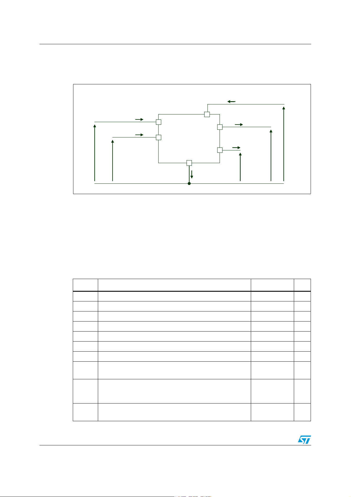
2 Electrical specifications
Figure 3. Current and voltage conventions
I
I
S
S
V
V
CC
GND
GND
CC
OUTPUT1,2
OUTPUT1,2
CURRENT
CURRENT
SENSE1,2
SENSE1,2
I
I
GND
GND
I
I
OUT1,2
OUT1,2
I
I
SENSE1,2
SENSE1,2
V
V
SENSE1,2
SENSE1,2
V
V
OUT1,2
OUT1,2
I
I
DE
DE
DE
DE
I
I
IN1,2
IN1,2
IN1,2
IN1,2
INPUT1,2
INPUT1,2
V
V
DE
DE
V
V
V
V
CC
CC
2.1 Absolute maximum ratings
Applying stress which exceeds above the ratings listed in Table 3: Absolute maximum
ratings may cause permanent damage to the device. These are stress ratings only and
operation of the device at these or any other conditions above those indicated in the
Operating sections of this specification is not implied. Exposure to the conditions in this
section for extended periods may affect device reliability. Refer also to the
STMicroelectronics SURE Program and other relevant quality documents.
Table 3. Absolute maximum ratings
Symbol Parameter Value Unit
V
V
CCPK
-V
I
OUT
- I
V
CSENSE
E
V
DC supply voltage 28 V
CC
Transient supply voltage (T < 400 ms, R
Reverse DC supply voltage 16 V
CC
DC output current Internally limited A
Reverse DC output current 70 A
OUT
I
DC input current -1 to 10 mA
IN
DC diagnostic enable input current -1 to 10 mA
I
DE
Current sense maximum voltage (VCC>0V)
Maximum switching energy (single pulse)
MAX
(L = 0.3 mH; R
I
OUT=IlimL
(Typ.))
=0Ω; V
L
=13.5V; T
bat
Electrostatic discharge
ESD
(Human Body Model: R = 1.5 kΩ; C=100pF)
>0.5Ω) 41 V
load
V
-41
CC
+V
CC
jstart
= 150 °C;
600 mJ
2000 V
V
V
8/45 Doc ID 17359 Rev 1
VND5E004A-E / VND5E004ASP30-E Electrical specifications
Table 3. Absolute maximum ratings (continued)
Symbol Parameter Value Unit
V
T
Charge device model (CDM-AEC-Q100-011) 750 V
ESD
T
Junction operating temperature -40 to 150 °C
j
Storage temperature -55 to 150 °C
STG
2.2 Thermal data
Table 4. Thermal data
Symbol Parameter
R
thj-case
R
thj-amb
1. PCB FR4 area 58 mm x 58 mm, PCB thickness 2 mm, Cu thickness 35 µm, minimum pad layout
2. PCB FR4 area 78 mm x 78 mm, PCB thickness 2 mm, Cu thickness 35 µm, minimum pad layout
Thermal resistance junction-case (with one
channel ON)
Thermal resistance junction-ambient 58
Maximum value
MultiPowerSO-30 12x12 PLLP
0.35 0.35 °C/W
(1)
39
(2)
Unit
°C/W
Doc ID 17359 Rev 1 9/45
Electrical specifications VND5E004A-E / VND5E004ASP30-E
2.3 Electrical characteristics
Values specified in this section are for 8 V < VCC<24V, -40°C <Tj<150°C, unless
otherwise stated.
Table 5. Power section
Symbol Parameter Test conditions Min. Typ. Max. Unit
V
V
V
USDhyst
R
R
ON REV
V
I
L(off)
1. For each channel
Operating supply voltage 4.5 13 28 V
CC
Undervoltage shutdown 3.5 4.5 V
USD
Undervoltage shutdown
hysteresis
On-state resistance
ON
R
DSon
condition
clampVCC
I
S
clamp voltage ICC=20mA; I
Supply current
Off-state output current
(1)
in reverse battery
I
=15A; Tj=25°C 3 mΩ
OUT
=15A; Tj= 150 °C 6 mΩ
I
OUT
I
=15A; VCC=5V; Tj=25°C 6 mΩ
OUT
VCC=-13V; I
=25°C
T
j
=-15A;
OUT
=0A 41 46 52 V
OUT1,2
Standby VDE=0V; VCC=13V;
=25°C; VIN=0;
T
j
V
OUT=VSENSE
Off-state; V
=5V; Tj=25°C;
V
DE
VIN=V
OUT=VSENSE
On-state; V
=5V; I
V
IN
=0V
=13V;
CC
=0V
=13V; VDE=5V;
CC
=0A
OUT
VIN=0V or VDE=0V; V
=13V; Tj= 25 °C 0 0.01 3 µA
V
CC
(1)
=0V or VDE=0V; V
V
IN
=13V; Tj=125°C
V
CC
OUT
OUT
=0V;
=0V;
0.5 V
3mΩ
25µA
10 15 µA
3.5 6 mA
05µA
10/45 Doc ID 17359 Rev 1
VND5E004A-E / VND5E004ASP30-E Electrical specifications
Table 6. Switching (VCC=13V; Tj=25°C)
Symbol Parameter Test conditions Min. Typ. Max. Unit
t
d(on)
t
d(off)
(dV
OUT
(dV
OUT
W
ON
W
OFF
Table 7. Logic inputs
Turn-on delay time RL= 0.87 Ω (see Ta bl e 6 )— 25 — µs
Turn-off delay time RL= 0.87 Ω (see Ta bl e 6 )— 35 — µs
/dt)onTurn-on voltage slope RL= 0.87 Ω —
/dt)
Turn-off voltage slope RL= 0.87 Ω —
off
Switching energy
losses during t
won
Switching energy
losses during t
woff
RL= 0.87 Ω (see Ta b le 6 )— 5.4 —mJ
RL= 0.87 Ω (see Ta b le 6)— 2.3 —mJ
See
Figure 26
See
Figure 28
—V/µs
—V/µs
Symbol Parameter Test conditions Min. Typ. Max. Unit
V
IL1,2
I
IL1,2
V
IH1,2
I
IH1,2
V
I(hyst)1,2
V
ICL1,2
V
DEL
I
DEL
V
DEH
I
DEH
V
DE(hyst)
V
DECL
Input low level voltage 0.9 V
Low level input current VIN=0.9V 1 µA
Input high level voltage 2.1 V
High level input current VIN=2.1V 10 µA
Input hysteresis voltage 0.25 V
I
=1mA 5.5 7 V
Input clamp voltage
IN
I
=-1mA -0.7 V
IN
DE low level voltage 0.9 V
DE low level current VIN=0.9V 1 µA
DE high level voltage 2.1 V
DE high level current VIN=2.1V 10 µA
DE hysteresis voltage 0.25 V
I
=1mA 5.5 7 V
DE clamp voltage
DE
=-1mA -0.7 V
I
DE
Doc ID 17359 Rev 1 11/45
Electrical specifications VND5E004A-E / VND5E004ASP30-E
Table 8. Protections and diagnostics
(1)
Symbol Parameter Test conditions Min. Typ. Max. Unit
I
limH
Short circuit current
VCC=13V
5V<VCC<24V
65 90
130
130
Short circuit current
I
limL
during thermal
VCC=13V; TR<Tj<T
TSD
40 A
cycling
T
T
T
V
DEMAG
V
1. To ensure long term reliability under heavy overload or short circuit conditions, protection and related
Shutdown
TSD
temperature
Reset temperature TRS+1 TRS+5 °C
T
R
Thermal reset of
RS
STATUS
Thermal hysteresis
HYST
(T
Turn-off output
voltage clamp
Output voltage drop
ON
limitation
diagnostic signals must be used together with a proper software strategy. If the device is subjected to
abnormal conditions, this software must limit the duration and number of activation cycles.
TSD-TR
)
=2A; VIN=0; L=6mH VCC-28 VCC-32 VCC-35 V
I
OUT
=1 A;
I
OUT
Tj= -40 °C to 150 °C
(see Figure 8)
150 175 200 °C
135 °C
7°C
25 mV
A
A
Table 9. Current sense (8 V < VCC<18V)
Symbol Parameter Test conditions Min. Typ. Max. Unit
I
K
K
dK
1/K1
K
dK2/K
I
0
OUT/ISENSE
I
1
OUT/ISENSE
Current sense ratio
(1)
drift
I
2
OUT/ISENSE
Current sense ratio
(1)
2
drift
=5 A; V
OUT
= -40 °C...150 °C
T
j
Tj= 25 °C...150 °C
I
=10A; V
OUT
5V;
= -40 °C...150 °C
T
j
T
= 25 °C...150 °C
j
=10 A; V
I
OUT
V
= 5 V;
DE
= -40 °C to 150 °C
T
j
I
=15A; V
OUT
Tj= -40 °C...150 °C
= 25 °C...150 °C
T
j
I
=15 A; V
OUT
5V;
= -40 °C to 150 °C
T
j
=4V; VDE= 5 V;
SENSE
=4V; VDE=
SENSE
=4V;
SENSE
=4V; VDE= 5 V;
SENSE
=4V; VDE=
SENSE
11420
12130
11830
12680
17580
17580
16910
16910
23740
23030
21990
21140
-14 +14 %
11760
13040
16110
16110
20460
19180
-10 +10 %
—
—
—
12/45 Doc ID 17359 Rev 1

VND5E004A-E / VND5E004ASP30-E Electrical specifications
Table 9. Current sense (8 V < VCC< 18 V) (continued)
Symbol Parameter Test conditions Min. Typ. Max. Unit
I
K
3
dK3/K
3
I
SENSE0
I
OL
V
SENSE
V
SENSEH
I
SENSEH
t
DSENSE1H
I
OUT/ISENSE
Current sense ratio
(1)
drift
Analog sense
leakage current
Open-load onstate current
detection threshold
Max analog sense
output voltage
Analog sense
output voltage in
fault condition
Analog sense
output current in
fault condition
Delay response
time from rising
edge of DE pin
=30A; V
OUT
5V;
= -40 °C...150 °C
T
j
= 25 °C...150 °C
T
j
I
=30 A; V
OUT
5V;
= -40 °C to 150 °C
T
j
I
=0A; V
OUT
SENSE
VDE= 0 V; VIN=0V;
= -40 °C...150 °C
T
j
I
=0A; V
OUT
= 5 V; VIN=5V;
V
DE
= -40 °C...150 °C
T
j
I
=15 A; V
OUT
=0V; VIN=5V;
V
DE
SENSE
VIN = 5V; 8V<VCC<18V
= 5 µA
I
SENSE
I
=45A; V
OUT
SENSE
SENSE
SENSE
=3.9kΩ
<4V, 5A<I
=90% of I
(2)
(2)
R
VCC=13 V; R
VCC=13 V; V
V
I
(see Figure 4)
=4V; VDE=
SENSE
SENSE
13040
13810
=4V; VDE=
15520
15520
18000
17230
-5 +5 %
=0V;
01µA
=0V;
02µA
=0V;
SENSE
01µA
10 150 mA
=0V;
CSD
=3.9kΩ 8V
SENSE
=5V 9 mA
SENSE
<30A
out
SENSE max
5V
50 100 µs
—
SENSE
SENSE
SENSE
SENSE
SENSE
SENSE
<4V, 5A<I
=10% of I
<4V, 5A<I
=90% of I
<4V, 5A<I
=10% of I
Delay response
t
DSENSE1L
time from falling
edge of DE pin
Delay response
t
DSENSE2H
time from rising
edge of INPUT pin
Delay response
t
DSENSE2L
time from falling
edge of INPUT pin
1. Parameter guaranteed by design; it is not tested.
2. Fault condition includes: power limitation, overtemperature and open-load off-state detection.
V
I
(see Figure 4)
V
I
VDE= 5 V (see Figure 4)
V
I
VDE= 5 V (see Figure 4)
<30A
out
SENSE max
<30A
out
SENSE max
<30A
out
SENSE max
520µs
200 600 µs
100 250 µs
Doc ID 17359 Rev 1 13/45
Electrical specifications VND5E004A-E / VND5E004ASP30-E
Table 10. Open-load detection (8V<VCC<18V, VDE= 5V)
Symbol Parameter Test conditions Min. Typ. Max. Unit
V
OL
t
DSTKON
I
L(off2)r
I
L(off2)f
td_vol
td_voh
Open-load off-state voltage
detection threshold
Output short circuit to VCC
detection delay at turn off
Off-state output current at
= 4 V
V
OUT
Off-state output current at
V
= 2 V
OUT
Delay response from output
rising edge to V
SENSE
rising
edge in open-load
Delay response from output
falling edge to V
SENSE
falling
edge in open-load
VIN = 0 V, VDE= 5 V;
See Figure 5
= 5 V; See Figure 5 180 — 1200 µs
V
DE
V
=0V; V
IN
SENSE
VDE= 5 V;
rising from 0 V to 4 V
V
OUT
V
=0V; V
IN
SENSE=VSENSEH
VDE= 5 V;
V
falling from VCC to 2 V
OUT
= 4 V; VIN= 0 V;
V
OUT
VDE= 5 V;
V
V
V
V
= 90% of V
SENSE
= 2 V; VIN= 0V;
OUT
= 5 V;
DE
= 10% of V
SENSE
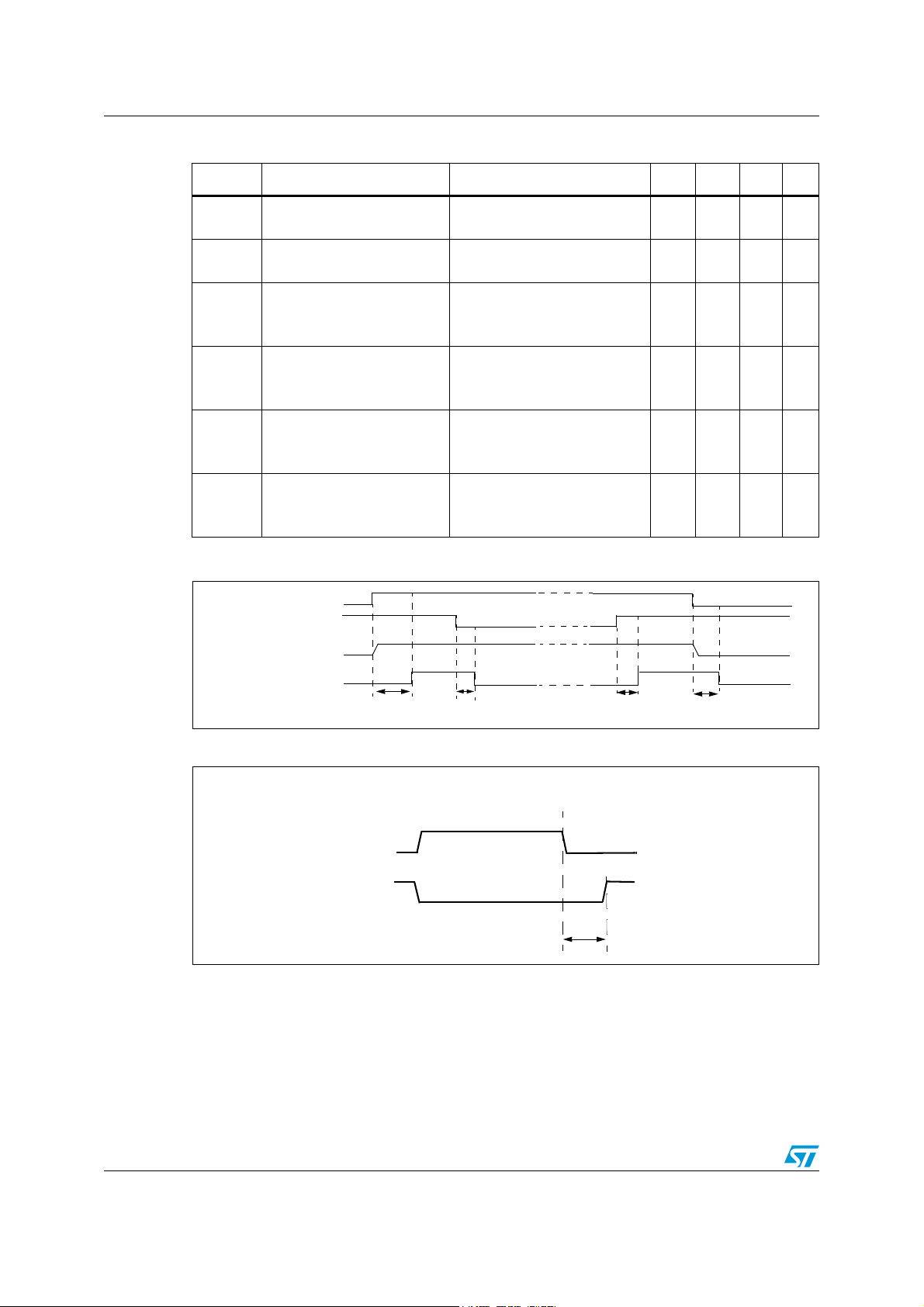
Figure 4. Current sense delay characteristics
INPUT
DE
LOAD CURRENT
2—4V
=0V;
-120 — 90 µA
-50 — 90 µA
—20µs
SENSEH
—20µs
SENSEH
SENSE CURRENT
t
DSENSE2H
t
DSENSE1L
Figure 5. Open-load off-state delay timing
OUTPUT STUCK AT V
V
IN
V
CS
CC
V
t
DSTKON
t
DSENSE1H
> V
OUT
V
SENSEH
OL
t
DSENSE2L
14/45 Doc ID 17359 Rev 1
 Loading...