

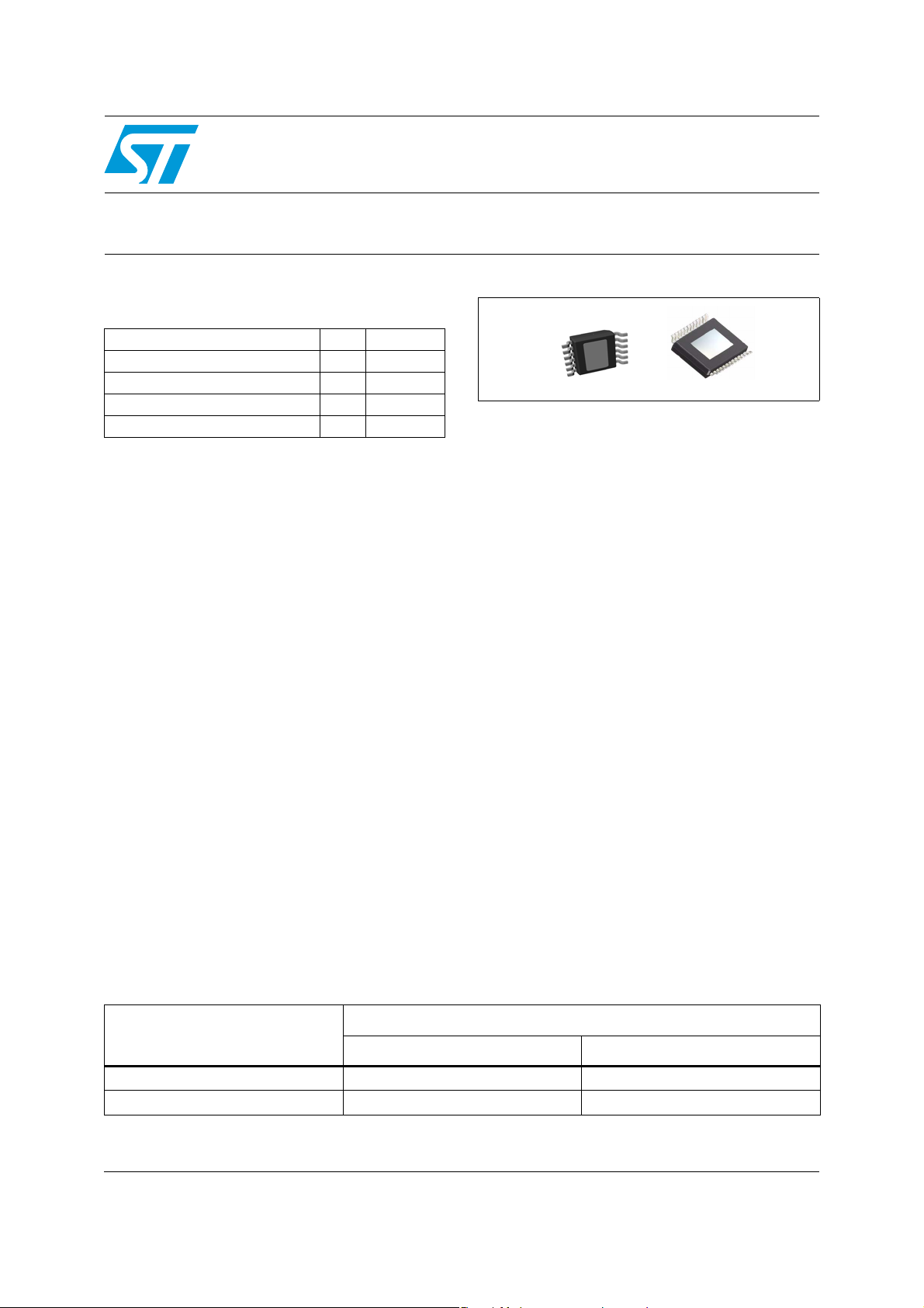
Features
VND5050J-E
VND5050K-E
Double channel high side driver
for automotive applications
Max supply voltage V
Operating voltage range V
Max on-State resistance (per ch.)
Current limitation (typ) I
Off-state supply current I
1. Typical value with all loads connected.
■ Main
– Inrush current active management by
power limitation
– Very low standby current
– 3.0 V CMOS compatible input
– Optimized electromagnetic emission
– Very low electromagnetic susceptibility
– In compliance with the 2002/95/EC
European directive
■ Diagnostic functions
– Open drain status output
– On-state open load detection
– Off-state open load detection
– Thermal shutdown indication
■ Protections
– Undervoltage shutdown
– Overvoltage clamp
– Output stuck to V
– Load current limitation
– Self limiting of fast thermal transients
– Protection against loss of ground and loss
of V
CC
– Thermal shutdown
Table 1. Device summary
Package
detection
CC
CC
CC
R
ON
LIMH
S
41 V
4.5 to 36 V
50 mΩ
18 A
(1)
2µA
PowerSSO-24PowerSSO-12
– Reverse battery protection (see Figure 28)
– Electrostatic discharge protection
Applications
■ All types of resistive, inductive and capacitive
loads
Description
The VND5050K-E and VND5050J-E are
monolithic devices made using
STMicroelectronics VIPower M0-5 technology.
they are intended for driving resistive or inductive
loads with one side connected to ground. Active
V
pin voltage clamp protects the devices
CC
against low energy spikes (see ISO7637 transient
compatibility table). The devices detect open load
condition both in on and off-state, when
STAT_DIS is left open or driven low. Output
shorted to V
When STAT_DIS is driven high, STATUS pin is in
high impedance state.
Output current limitation protects the devices in
overload condition. In case of long overload
duration, the devices limit the dissipated power to
a safe level up to thermal shutdown intervention.
Thermal shutdown with automatic restart allows
the devices to recover normal operation as soon
as fault conditions disappear.
Tub e Tap e a nd reel
is detected in the off-state.
CC
Order code
PowerSSO-12 VND5050J-E VND5050JTR-E
PowerSSO-24 VND5050K-E VND5050KTR-E
July 2009 Doc ID 12266 Rev 6 1/37
www.st.com
1

Contents VND5050J-E / VND5050K-E
Contents
1 Block diagram and pin description . . . . . . . . . . . . . . . . . . . . . . . . . . . . . 5
2 Electrical specifications . . . . . . . . . . . . . . . . . . . . . . . . . . . . . . . . . . . . . . 7
2.1 Absolute maximum ratings . . . . . . . . . . . . . . . . . . . . . . . . . . . . . . . . . . . . . 7
2.2 Thermal data . . . . . . . . . . . . . . . . . . . . . . . . . . . . . . . . . . . . . . . . . . . . . . . 8
2.3 Electrical characteristics . . . . . . . . . . . . . . . . . . . . . . . . . . . . . . . . . . . . . . . 8
2.4 Electrical characteristics curves . . . . . . . . . . . . . . . . . . . . . . . . . . . . . . . . 16
3 Application information . . . . . . . . . . . . . . . . . . . . . . . . . . . . . . . . . . . . . 20
3.1 GND protection network against reverse battery . . . . . . . . . . . . . . . . . . . 20
3.1.1 Solution 1: resistor in the ground line (RGND only) . . . . . . . . . . . . . . . . 20
3.1.2 Solution 2: a diode (DGND) in the ground line . . . . . . . . . . . . . . . . . . . 21
3.2 Load dump protection . . . . . . . . . . . . . . . . . . . . . . . . . . . . . . . . . . . . . . . . 21
3.3 Microcontroller I/Os protection . . . . . . . . . . . . . . . . . . . . . . . . . . . . . . . . . 21
3.4 Open-load detection in off-state . . . . . . . . . . . . . . . . . . . . . . . . . . . . . . . . 21
3.5 Maximum demagnetization energy (VCC = 13.5V) . . . . . . . . . . . . . . . . . 23
4 Package and PCB thermal data . . . . . . . . . . . . . . . . . . . . . . . . . . . . . . . 24
4.1 PowerSSO-12™ thermal data . . . . . . . . . . . . . . . . . . . . . . . . . . . . . . . . . 24
4.2 PowerSSO-24™ thermal data . . . . . . . . . . . . . . . . . . . . . . . . . . . . . . . . . 27
5 Package and packing information . . . . . . . . . . . . . . . . . . . . . . . . . . . . . 30
5.1 ECOPACK® packages . . . . . . . . . . . . . . . . . . . . . . . . . . . . . . . . . . . . . . . 30
5.2 PowerSSO-12™ package information . . . . . . . . . . . . . . . . . . . . . . . . . . . 30
5.3 PowerSSO-24™ package information . . . . . . . . . . . . . . . . . . . . . . . . . . . 32
5.4 PowerSSO-12™ packing information . . . . . . . . . . . . . . . . . . . . . . . . . . . . 34
5.5 PowerSSO-24™ packing information . . . . . . . . . . . . . . . . . . . . . . . . . . . . 35
6 Revision history . . . . . . . . . . . . . . . . . . . . . . . . . . . . . . . . . . . . . . . . . . . 36
2/37 Doc ID 12266 Rev 6

VND5050J-E / VND5050K-E List of tables
List of tables
Table 2. Pin function . . . . . . . . . . . . . . . . . . . . . . . . . . . . . . . . . . . . . . . . . . . . . . . . . . . . . . . . . . . . . . 5
Table 3. Suggested connections for unused and not connected pins . . . . . . . . . . . . . . . . . . . . . . . . 6
Table 4. Absolute maximum ratings . . . . . . . . . . . . . . . . . . . . . . . . . . . . . . . . . . . . . . . . . . . . . . . . . . 7
Table 5. Thermal data. . . . . . . . . . . . . . . . . . . . . . . . . . . . . . . . . . . . . . . . . . . . . . . . . . . . . . . . . . . . . 8
Table 6. Power section . . . . . . . . . . . . . . . . . . . . . . . . . . . . . . . . . . . . . . . . . . . . . . . . . . . . . . . . . . . . 8
Table 7. Switching (VCC = 13V; Tj = 25°C) . . . . . . . . . . . . . . . . . . . . . . . . . . . . . . . . . . . . . . . . . . . . 9
Table 8. Status pin (V
Table 9. Protections . . . . . . . . . . . . . . . . . . . . . . . . . . . . . . . . . . . . . . . . . . . . . . . . . . . . . . . . . . . . . 10
Table 10. Openload detection. . . . . . . . . . . . . . . . . . . . . . . . . . . . . . . . . . . . . . . . . . . . . . . . . . . . . . . 10
Table 11. Logic input . . . . . . . . . . . . . . . . . . . . . . . . . . . . . . . . . . . . . . . . . . . . . . . . . . . . . . . . . . . . . 10
Table 12. Truth table. . . . . . . . . . . . . . . . . . . . . . . . . . . . . . . . . . . . . . . . . . . . . . . . . . . . . . . . . . . . . . 12
Table 13. Electrical transient requirements (part 1/3) . . . . . . . . . . . . . . . . . . . . . . . . . . . . . . . . . . . . . 13
Table 14. Electrical transient requirements (part 2/3) . . . . . . . . . . . . . . . . . . . . . . . . . . . . . . . . . . . . . 13
Table 15. Electrical transient requirements (part 3/3) . . . . . . . . . . . . . . . . . . . . . . . . . . . . . . . . . . . . . 14
Table 16. PowerSSO-12™ thermal parameters . . . . . . . . . . . . . . . . . . . . . . . . . . . . . . . . . . . . . . . . . 26
Table 17. PowerSSO-24™ thermal parameters . . . . . . . . . . . . . . . . . . . . . . . . . . . . . . . . . . . . . . . . . 29
Table 18. PowerSSO-12™ mechanical data . . . . . . . . . . . . . . . . . . . . . . . . . . . . . . . . . . . . . . . . . . . 31
Table 19. PowerSSO-24™ mechanical data . . . . . . . . . . . . . . . . . . . . . . . . . . . . . . . . . . . . . . . . . . . 32
Table 20. Document revision history . . . . . . . . . . . . . . . . . . . . . . . . . . . . . . . . . . . . . . . . . . . . . . . . . 36
=0V) . . . . . . . . . . . . . . . . . . . . . . . . . . . . . . . . . . . . . . . . . . . . . . . . . . . . . . . 9
SD
Doc ID 12266 Rev 6 3/37

List of figures VND5050J-E / VND5050K-E
List of figures
Figure 1. Block diagram . . . . . . . . . . . . . . . . . . . . . . . . . . . . . . . . . . . . . . . . . . . . . . . . . . . . . . . . . . . . 5
Figure 2. Configuration diagram (top view) . . . . . . . . . . . . . . . . . . . . . . . . . . . . . . . . . . . . . . . . . . . . . 6
Figure 3. Current and voltage conventions . . . . . . . . . . . . . . . . . . . . . . . . . . . . . . . . . . . . . . . . . . . . . 7
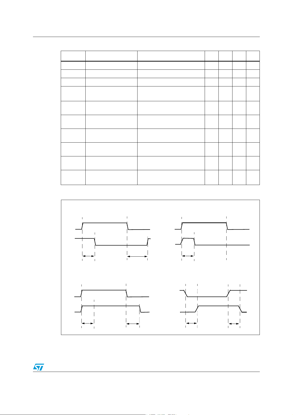
Figure 4. Status timings . . . . . . . . . . . . . . . . . . . . . . . . . . . . . . . . . . . . . . . . . . . . . . . . . . . . . . . . . . . 11
Figure 5. Switching characteristics . . . . . . . . . . . . . . . . . . . . . . . . . . . . . . . . . . . . . . . . . . . . . . . . . . 12
Figure 6. Output voltage drop limitation . . . . . . . . . . . . . . . . . . . . . . . . . . . . . . . . . . . . . . . . . . . . . . . 13
Figure 7. Waveforms . . . . . . . . . . . . . . . . . . . . . . . . . . . . . . . . . . . . . . . . . . . . . . . . . . . . . . . . . . . . . 15
Figure 8. Off-state output current . . . . . . . . . . . . . . . . . . . . . . . . . . . . . . . . . . . . . . . . . . . . . . . . . . . . 16
Figure 9. High level input current . . . . . . . . . . . . . . . . . . . . . . . . . . . . . . . . . . . . . . . . . . . . . . . . . . . . 16
Figure 10. Input clamp voltage. . . . . . . . . . . . . . . . . . . . . . . . . . . . . . . . . . . . . . . . . . . . . . . . . . . . . . . 16
Figure 11. Input high level . . . . . . . . . . . . . . . . . . . . . . . . . . . . . . . . . . . . . . . . . . . . . . . . . . . . . . . . . . 16
Figure 12. Input low level . . . . . . . . . . . . . . . . . . . . . . . . . . . . . . . . . . . . . . . . . . . . . . . . . . . . . . . . . . . 16
Figure 13. Input hysteresis voltage . . . . . . . . . . . . . . . . . . . . . . . . . . . . . . . . . . . . . . . . . . . . . . . . . . . 16
Figure 14. Status low output voltage . . . . . . . . . . . . . . . . . . . . . . . . . . . . . . . . . . . . . . . . . . . . . . . . . . 17
Figure 15. On-state resistance vs T
Figure 16. Status leakage current . . . . . . . . . . . . . . . . . . . . . . . . . . . . . . . . . . . . . . . . . . . . . . . . . . . . 17
Figure 17. On-state resistance vs V
Figure 18. Status clamp voltage . . . . . . . . . . . . . . . . . . . . . . . . . . . . . . . . . . . . . . . . . . . . . . . . . . . . . 17
Figure 19. Openload on-state detection threshold . . . . . . . . . . . . . . . . . . . . . . . . . . . . . . . . . . . . . . . . 17
Figure 20. Openload off-state voltage detection threshold . . . . . . . . . . . . . . . . . . . . . . . . . . . . . . . . . 18
Figure 21. I
LIM
vs T
. . . . . . . . . . . . . . . . . . . . . . . . . . . . . . . . . . . . . . . . . . . . . . . . . . . . . . . . . . . . 18
case
Figure 22. Turn-on voltage slope . . . . . . . . . . . . . . . . . . . . . . . . . . . . . . . . . . . . . . . . . . . . . . . . . . . . . 18
Figure 23. Undervoltage shutdown . . . . . . . . . . . . . . . . . . . . . . . . . . . . . . . . . . . . . . . . . . . . . . . . . . . 18
Figure 24. Turn-off voltage slope . . . . . . . . . . . . . . . . . . . . . . . . . . . . . . . . . . . . . . . . . . . . . . . . . . . . . 18
Figure 25. STAT_DIS clamp voltage . . . . . . . . . . . . . . . . . . . . . . . . . . . . . . . . . . . . . . . . . . . . . . . . . . 18
Figure 26. High level STAT_DIS voltage . . . . . . . . . . . . . . . . . . . . . . . . . . . . . . . . . . . . . . . . . . . . . . . 19
Figure 27. Low level STAT_DIS voltage . . . . . . . . . . . . . . . . . . . . . . . . . . . . . . . . . . . . . . . . . . . . . . . 19
Figure 28. Application schematic . . . . . . . . . . . . . . . . . . . . . . . . . . . . . . . . . . . . . . . . . . . . . . . . . . . . . 20
Figure 29. Open-load detection in off-state . . . . . . . . . . . . . . . . . . . . . . . . . . . . . . . . . . . . . . . . . . . . . 22
Figure 30. Maximum turn-off current versus inductance (for each channel) . . . . . . . . . . . . . . . . . . . . 23
Figure 31. PowerSSO-12™ PC board . . . . . . . . . . . . . . . . . . . . . . . . . . . . . . . . . . . . . . . . . . . . . . . . . 24
Figure 32. Rthj-amb vs PCB copper area in open box free air condition (one channel on). . . . . . . . . 24
Figure 33. PowerSSO-12™ thermal impedance junction ambient single pulse (one channel on). . . . 25
Figure 34. Thermal fitting model of a double channel HSD in PowerSSO-12™ . . . . . . . . . . . . . . . . . 25
Figure 35. PowerSSO-24™ PC board . . . . . . . . . . . . . . . . . . . . . . . . . . . . . . . . . . . . . . . . . . . . . . . . . 27
Figure 36. Rthj-amb vs PCB copper area in open box free air condition (one channel on). . . . . . . . . 27
Figure 37. PowerSSO-24™ thermal impedance junction ambient single pulse (one channel on). . . . 28
Figure 38. Thermal fitting model of a double channel HSD in PowerSSO-24™ . . . . . . . . . . . . . . . . . 28
Figure 39. PowerSSO-12™ package dimensions . . . . . . . . . . . . . . . . . . . . . . . . . . . . . . . . . . . . . . . . 30
Figure 40. PowerSSO-24™ package dimensions . . . . . . . . . . . . . . . . . . . . . . . . . . . . . . . . . . . . . . . . 32
Figure 41. PowerSSO-12™ tube shipment (no suffix) . . . . . . . . . . . . . . . . . . . . . . . . . . . . . . . . . . . . . 34
Figure 42. PowerSSO-12™ tape and reel shipment (suffix “TR”) . . . . . . . . . . . . . . . . . . . . . . . . . . . . 34
Figure 43. PowerSS0-24™
Figure 44. PowerSSO-24™
tube shipment (no suffix) . . . . . . . . . . . . . . . . . . . . . . . . . . . . . . . . . . . . . 35
tape and reel shipment (suffix “TR”) . . . . . . . . . . . . . . . . . . . . . . . . . . . . 35
. . . . . . . . . . . . . . . . . . . . . . . . . . . . . . . . . . . . . . . . . . . . . . . . 17
case
. . . . . . . . . . . . . . . . . . . . . . . . . . . . . . . . . . . . . . . . . . . . . . . . . 17
CC
4/37 Doc ID 12266 Rev 6
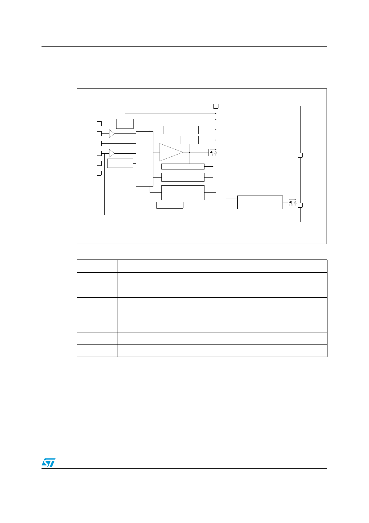
VND5050J-E / VND5050K-E Block diagram and pin description
1 Block diagram and pin description
Figure 1. Block diagram
V
CC
V
GND
INPUT1
STATUS1
STAT_DIS
INPUT2
STATUS2
CC
CLAMP
OVE RTE MP. 1
LOGIC
UNDERVOLTAGE
CLAMP 1
DRIVER 1
CURRENT LIMITER 1
OPENLOAD ON 1
OUTPUT1
OPENLOAD OFF 1
PWR
1
LIM
Table 2. Pin function
Name Function
V
CC
Battery connection.
OUTPUTn Power output.
GND
INPUTn
Ground connection. Must be reverse battery protected by an external diode/resistor
network.
Voltage controlled input pin with hysteresis, CMOS compatible. Controls output
switch state.
STATUSn Open drain digital diagnostic pin.
STAT_DIS
Active high CMOS compatible pin, to disable the STATUS pin.
INPUT2
CONTROL & PROTECTION
EQUIVALENT TO
STATUS2
CHANNEL1
V
CC
OUTPUT2
Doc ID 12266 Rev 6 5/37
Block diagram and pin description VND5050J-E / VND5050K-E
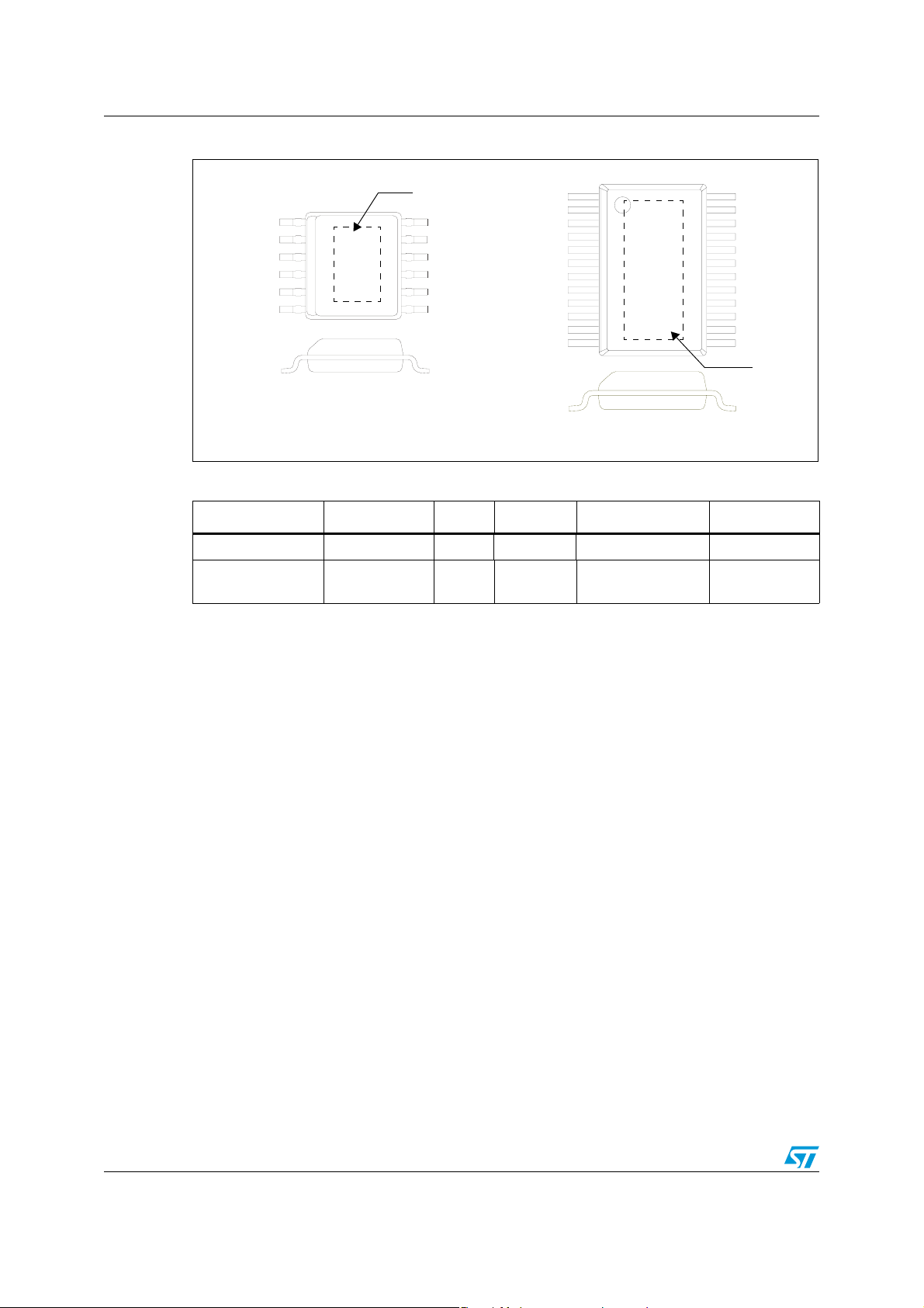
Figure 2. Configuration diagram (top view)
TA B = V
GND
STAT_DIS
INPUT 1
STATUS 1
STATUS 2
INPUT 2
cc
1
2
3
4
5
6
12
11
10
9
8
7
V
cc
OUTPUT 1
OUTPUT 1
OUTPUT 2
OUTPUT 2
V
cc
V
GND.
N.C.
STAT_DIS
INPUT1
STATUS1
N.C.
STATUS2
N.C.
INPUT2
N.C.
V
CC
CC
OUTPUT1
OUTPUT1
OUTPUT1
OUTPUT1
OUTPUT1
OUTPUT1
OUTPUT2
OUTPUT2
OUTPUT2
OUTPUT2
OUTPUT2
OUTPUT2
TAB = V
CC
PowerSSO-12
Table 3. Suggested connections for unused and not connected pins
PowerSSO-24
Connection/pin STATUS N.C. OUTPUT INPUT STAT_DIS
Floating X X X X X
To ground N.R.
1. Not recommended.
(1)
XN.R.
Through 10KΩ
resistor
Through 10KΩ
resistor
6/37 Doc ID 12266 Rev 6
VND5050J-E / VND5050K-E Electrical specifications
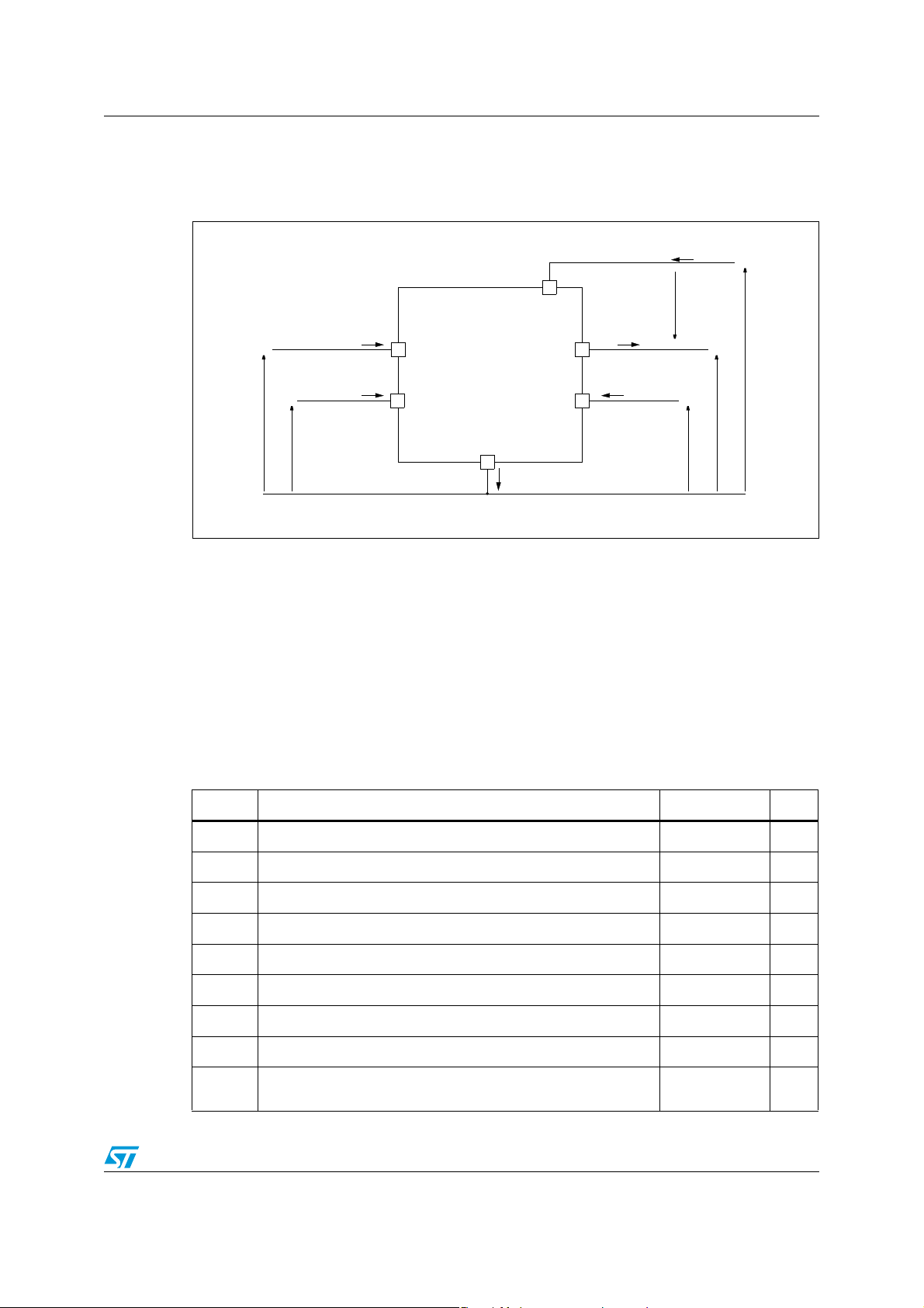
2 Electrical specifications
Figure 3. Current and voltage conventions
I
S
V
CC
V
CC
Fn
V
I
SD
V
SD
I
INn
INPUTn
V
INn
Note: V
Fn
= V
OUTn
- V
during reverse battery condition.
CCn
2.1 Absolute maximum ratings
Stressing the device above the rating listed in the “Absolute maximum ratings” table may
cause permanent damage to the device. These are stress ratings only and operation of the
device at these or any other conditions above those indicated in the Operating sections of
this specification is not implied. Exposure to the conditions in table below for extended
periods may affect device reliability. Refer also to the STMicroelectronics SURE Program
and other relevant quality document.
Table 4. Absolute maximum ratings
Symbol Parameter Value Unit
GND
OUTPUTnSTAT_DIS
STATUSn
I
GND
I
OUTn
I
STATn
V
STATn
V
OUTn
V
- V
- I
I
OUT
- I
I
STAT
I
STAT_DIS
E
DC supply voltage 41 V
CC
Reverse DC supply voltage 0.3 V
CC
DC reverse ground pin current 200 mA
GND
DC output current Internally limited A
Reverse dc output current 15 A
OUT
DC input current +10 / -1 mA
I
IN
DC status current +10 / -1 mA
DC status disable current +10 / -1 mA
Maximum switching energy
MAX
(L=3mH; RL=0Ω; V
=13.5V; T
bat
jstart
=150ºC; I
OUT
= I
limL
(Typ.))
104 mJ
Doc ID 12266 Rev 6 7/37
Electrical specifications VND5050J-E / VND5050K-E
Table 4. Absolute maximum ratings (continued)
Symbol Parameter Value Unit
Electrostatic discharge (Human Body Model: R=1.5KΩ;
C=100pF)
– Input
ESD
– Status
V
–STAT_DIS
– Output
–V
CC
V
Charge device model (CDM-AEC-Q100-011) 750 V
ESD
T
Junction operating temperature -40 to 150 °C
j
4000
4000
4000
5000
5000
V
V
V
V
V
T
Storage temperature - 55 to 150 °C
stg
2.2 Thermal data
Table 5. Thermal data
Symbol Parameter
R
thj-case
R
thj-amb
Thermal resistance junction case (max)
(with one channel on)
Thermal resistance junction ambient
(max)
2.3 Electrical characteristics
8V<VCC<36 V; -40 °C<Tj<150 °C, unless otherwise specified.
.
Table 6. Power section
Symbol Parameter Test conditions Min. Typ. Max. Unit
V
V
USD
V
USDhyst
Operating supply voltage 4.5 13 36 V
CC
Undervoltage shutdown 3.5 4.5 V
Undervoltage shutdown
hysteresis
Value
Unit
PowerSSO-12 PowerSSO-24
2.8 2.8 °C/W
See Figure 32 See Figure 36 °C/W
0.5 V
I
R
On-state resistance
ON
(2)
I
I
V
clamp
Clamp voltage IS=20mA 41 46 52 V
Off-state; V
S
Supply current
I
VIN=V
On-state; V
I
8/37 Doc ID 12266 Rev 6
=2A; Tj=25°C
OUT
=2A; Tj=150°C
OUT
=2A; VCC=5V; Tj=25°C
OUT
=13V; Tj=25°C;
CC
OUT=VSENSE=VCSD
=13V; VIN=5V;
CC
=0A
OUT
=0V
50
mΩ
100
mΩ
65
mΩ
(1)
(1)
5
2
3
6µAmA
VND5050J-E / VND5050K-E Electrical specifications
Table 6. Power section (continued)
Symbol Parameter Test conditions Min. Typ. Max. Unit
I
L(off1)
I
L(off2)
V
Off-state output
current
Off-state output
current
Output - VCC diode
F
voltage
(2)
(2)
(2)
VIN=V
=25°C
T
j
VIN=V
=125°C
T
j
VIN=0V; V
-I
OUT
=0V; VCC=13V;
OUT
000.01 3
=0V; VCC=13V;
OUT
=4V -75 0
OUT
5
=4A; Tj=150°C 0.7 V
1. PowerMOS leakage included.
2. For each channel.
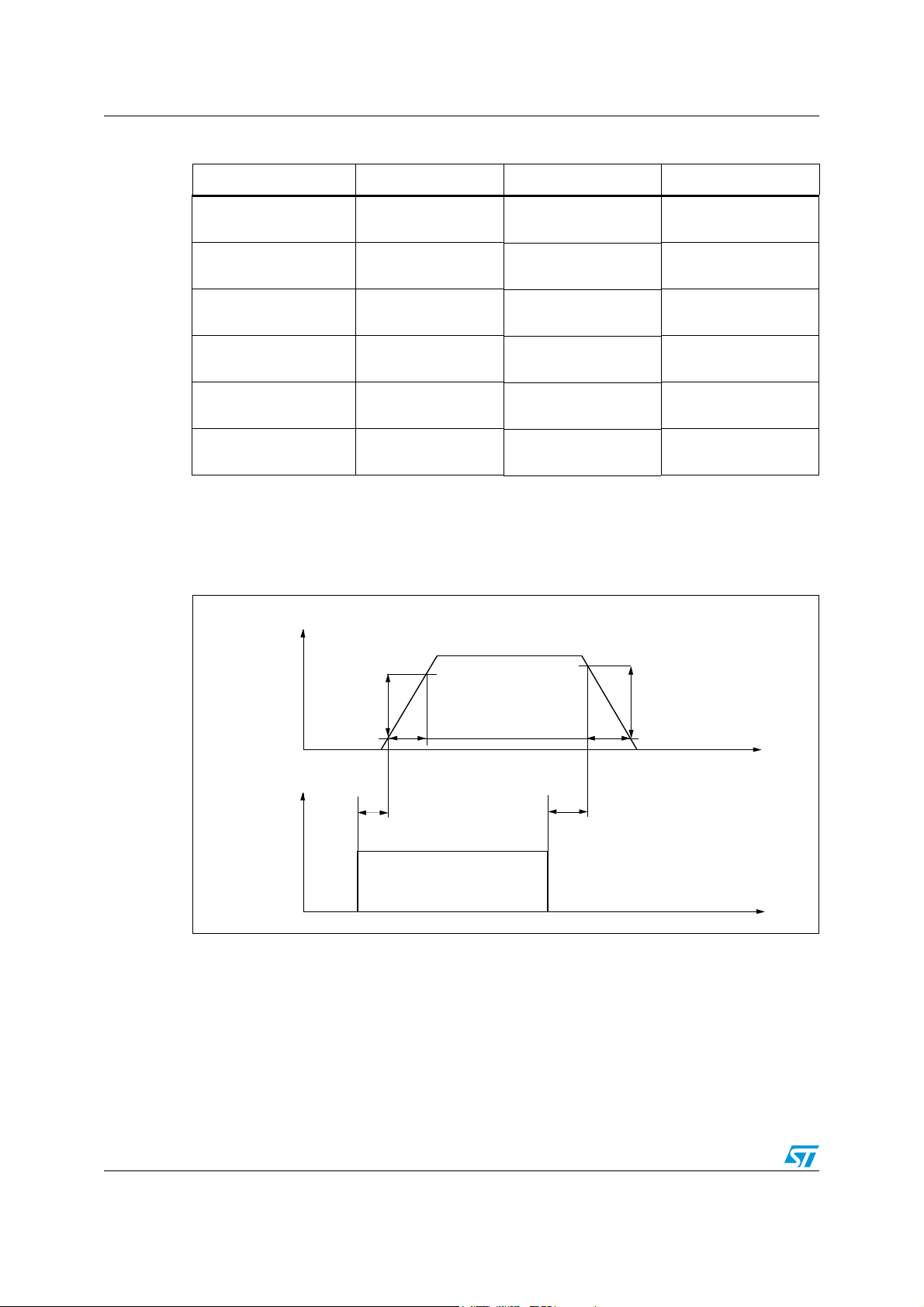
Table 7. Switching (VCC=13V; Tj= 25°C)
Symbol Parameter Test conditions Min. Typ. Max. Unit
dV
dV
t
d(on)
t
d(off)
OUT
OUT
W
W
/dt
/dt
ON
OFF
Turn-on delay time RL= 6.5Ω (see Figure 5)20µs
Turn-off delay time RL= 6.5Ω (see Figure 5)40µs
Turn-on voltage slope RL= 6.5Ω See Figure 22 V/µs
(on)
Turn-off voltage slope RL= 6.5Ω See Figure 24 V/µs
(off)
Switching energy losses
during t
won
Switching energy losses
during t
woff
RL= 6.5Ω (see Figure 5)0.21mJ
RL= 6.5Ω (see Figure 5)0.28mJ
µA
Table 8. Status pin (VSD=0V)
Symbol Parameter Test conditions Min. Typ. Max. Unit
V
STAT
I
LSTAT
C
STAT
V
Status low output
voltage
Status leakage current
Status pin input
capacitance
Status clamp voltage
SCL
= 1.6 mA, VSD=0V 0.5 V
I
STAT
Normal operation or V
= 5V
V
STAT
SD
=5V,
Normal operation or VSD=5V,
V
= 5V
STAT
= 1mA
I
STAT
I
STAT
= -1mA
5.5
-0.7
10 µA
100 pF
7V
V
Doc ID 12266 Rev 6 9/37
Electrical specifications VND5050J-E / VND5050K-E
Table 9. Protections
(1)
Symbol Parameter Test conditions Min. Typ. Max. Unit
I
limH
I
limL
T
TSD
T
T
RS
T
HYST
t
SDL
V
DEMAG
V
ON
1. To ensure long term reliability under heavy overload or short circuit conditions, protection and related
diagnostic signals must be used together with a proper software strategy. If the device is subjected to
abnormal conditions, this software must limit the duration and number of activation cycles.
DC short circuit current
Short circuit current
during thermal cycling
Shutdown temperature 150 175 200 °C
Reset temperature
R
Thermal reset of STATUS 135 °C
Thermal hysteresis
(T
TSD-TR
)
Status delay in overload
conditions
Turn-off output voltage
clamp
Output voltage drop
limitation
VCC=13V
5V<VCC<36V
=13V
V
CC
TR<Tj<T
T
I
OUT
I
OUT
T
TSD
(see Figure 4)20µs
j>TTSD
=2A; VIN=0; L=6mH
= 0.1A;
= -40°C...+150°C
j
(see Figure 6)
12 18 24
24
7A
TRS + 1 TRS + 5
7°C
VCC-41 VCC-46 VCC-52
25 mV
A
A
°C
V
Table 10. Openload detection
Symbol Parameter Test conditions Min. Typ. Max. Unit
I
OL
t
DOL(on)
Openload on-state
detection threshold
Openload on-state
detection delay
= 5V,8V<VCC<18V 10
V
IN
I
= 0A, VCC=13V
OUT
(see Figure 4)
See
Figure 19
70 mA
200 µs
Delay between INPUT
t
POL
falling edge and STATUS
rising edge in Openload
= 0A (see Figure 4) 200 500 1000 µs
I
OUT
condition
Openload off-state
V
voltage detection
OL
V
= 0V, 8V<VCC<16V 2
IN
threshold
See
Figure 20
4V
Output short circuit to
t
DSTKON
V
detection delay at
CC
(see Figure 4)180t
POL
µs
turn-off
Table 11. Logic input
Symbol Parameter Test conditions Min. Typ. Max. Unit
V
I
Input low level 0.9 V
IL
Low level input current VIN =0.9 V 1 µA
IL
10/37 Doc ID 12266 Rev 6
VND5050J-E / VND5050K-E Electrical specifications
Table 11. Logic input (continued)
Symbol Parameter Test conditions Min. Typ. Max. Unit
V
I
V
I(hyst)
V
ICL
V
SDL
I
SDL
V
SDH
I
SDH
V
SD(hyst)
V
SDCL
Input high level 2.1 V
IH
High level input current VIN = 2.1 V 10 µA
IH
Input hysteresis voltage 0.25 V
Input clamp voltage
STAT_DIS low level
voltage
Low level STAT_DIS
current
STAT_DIS high level
voltage
High level STAT_DIS
current
STAT_DIS hysteresis
voltage
STAT_DIS clamp voltage
Figure 4. Status timings
I
= 1mA
IN
= -1mA
I
IN
V
= 0.9 V 1 µA
SD
5.5
-0.7
2.1 V
= 2.1 V 10 µA
V
SD
0.25 V
ISD= 1mA
= -1mA
I
SD
5.5
-0.7
7V
V
0.9 V
7V
V
OPEN LOAD STATUS TIMING (without external pull-up)
I
< I
OUT
I
OUT
> I
OL
OL
V
t
CC
V
t
DSTKON
OUT
POL
OUT
< V
> V
OL
OL
V
IN
V
STAT
t
DOL(on)
OUTPUT STUCK TO V
V
IN
V
STAT
t
DOL(on)
OPEN LOAD STATUS TIMING (with external pull-up)
I
< I
OUT
V
V
IN
STAT
t
DOL(on)
OL
V
OUT
> V
OL
OVER TEMP STATUS TIMING
Tj > T
V
V
IN
STAT
t
SDL
TSD
t
SDL
Doc ID 12266 Rev 6 11/37
Electrical specifications VND5050J-E / VND5050K-E
Table 12. Truth table
Conditions Input Output Sense (V
Normal operation
L
H
L
H
CSD
H
H
=0V)
(1)
Current limitation
Over temperature
Undervoltage
Output voltage > V
Output current < I
1. If the V
and external circuit.
is high, the SENSE output is at a high impedance, its potential depends on leakage currents
CSD
OL
OL
L
H
L
H
L
H
L
H
L
H
L
X
L
L
L
L
H
H
L
H
2. The STATUS pin is low with a delay equal to tDSTKON after INPUT falling edge.
3. The STATUS pin becomes high with a delay equal to tPOL after INPUT falling edge.
Figure 5. Switching characteristics
V
OUT
90%
t
f
dV
OUT
dV
OUT
/dt
(on)
80%
t
r
10%
/dt
(off)
H
H
H
H
L
X
X
(2)
L
H
(3)
L
t
INPUT
t
d(on)
12/37 Doc ID 12266 Rev 6
t
d(off)
t
 Loading...