


查询VND05B供应商
VND05B
/ VND05B (011Y) / VND05B (012Y)
HIGH SIDE SMART POWER SOLID STATE RELAY
TYPE V
VND05B
VND05B (011Y)
VND05B (012Y)
■ OUTPUT CURRENT (CONTINUOUS): 9A AT
DSSRDS(on)In
40V 200mΩ 1.6A 26 V
Tc=85°C PER CHANNEL
■ 5V LOGIC LEVEL COMPATIBLE INPUT
■ THERMAL SHUT-DOWN
■ UNDERVOLTAGE PROTECTION
■ OPEN DRAIN DIAGNOSTIC OUTPUT
■ INDUCTIVE LOAD FAST DEMAGNETIZATION
■ VERY LOW STAND-BYPOWER DISSIPATION
DESCRIPTION
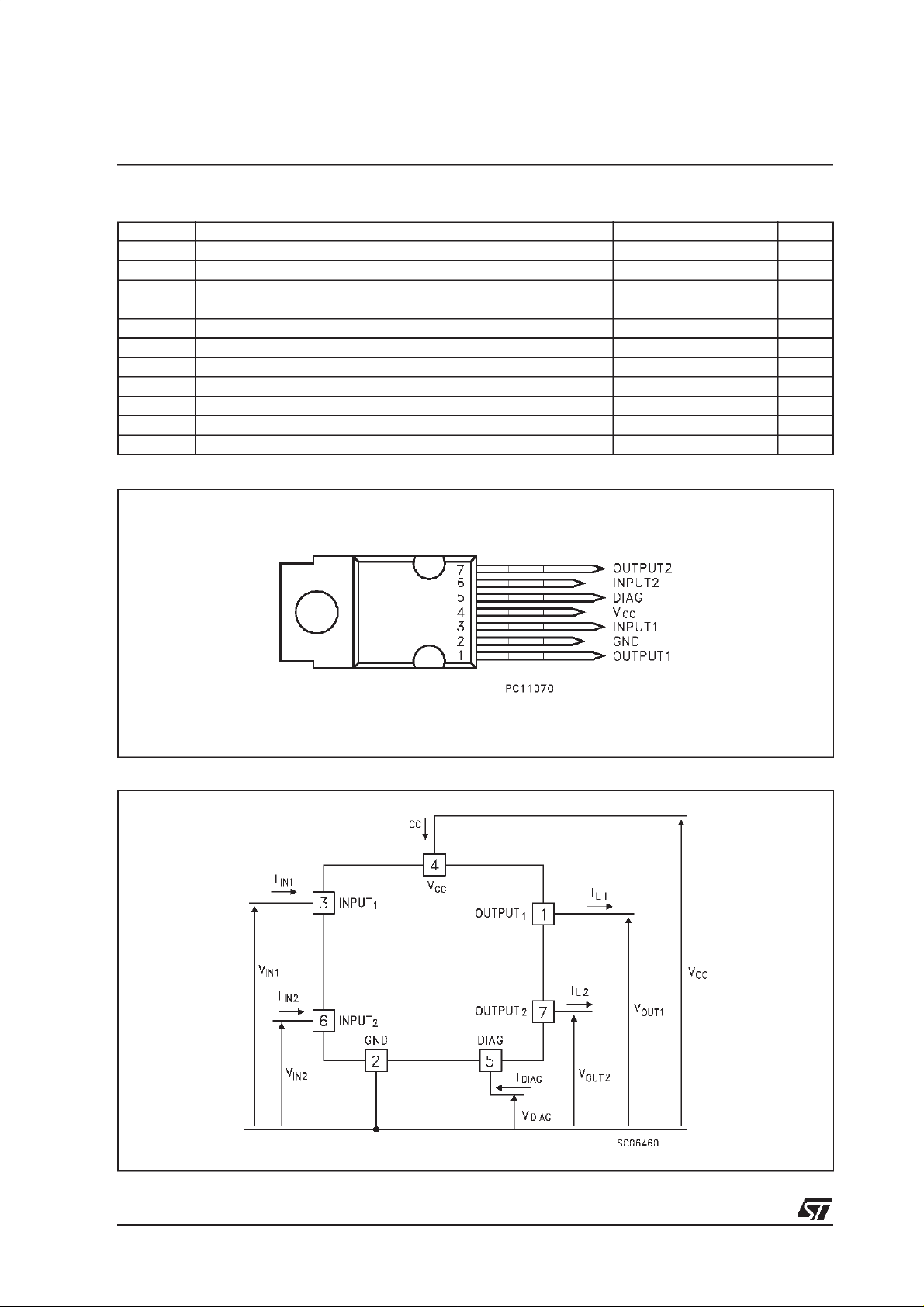
The VND05B, VND05B (011Y), VND05B (012Y) is
a monolithic device designed in
STMicroelectronics VIPower technology, intended
for driving resistive or inductive loads with one
side connected to ground. This device has two
channels, and a common diagnostic. Built-in
thermal shutdown protects the chip from
overtemperature and short circuit. The status
output provides an indication of open load in on
state, open load in off state, overtemperature
conditions and stuck-on to VCC.
(*) V
CC
DOUBLE CHANNEL
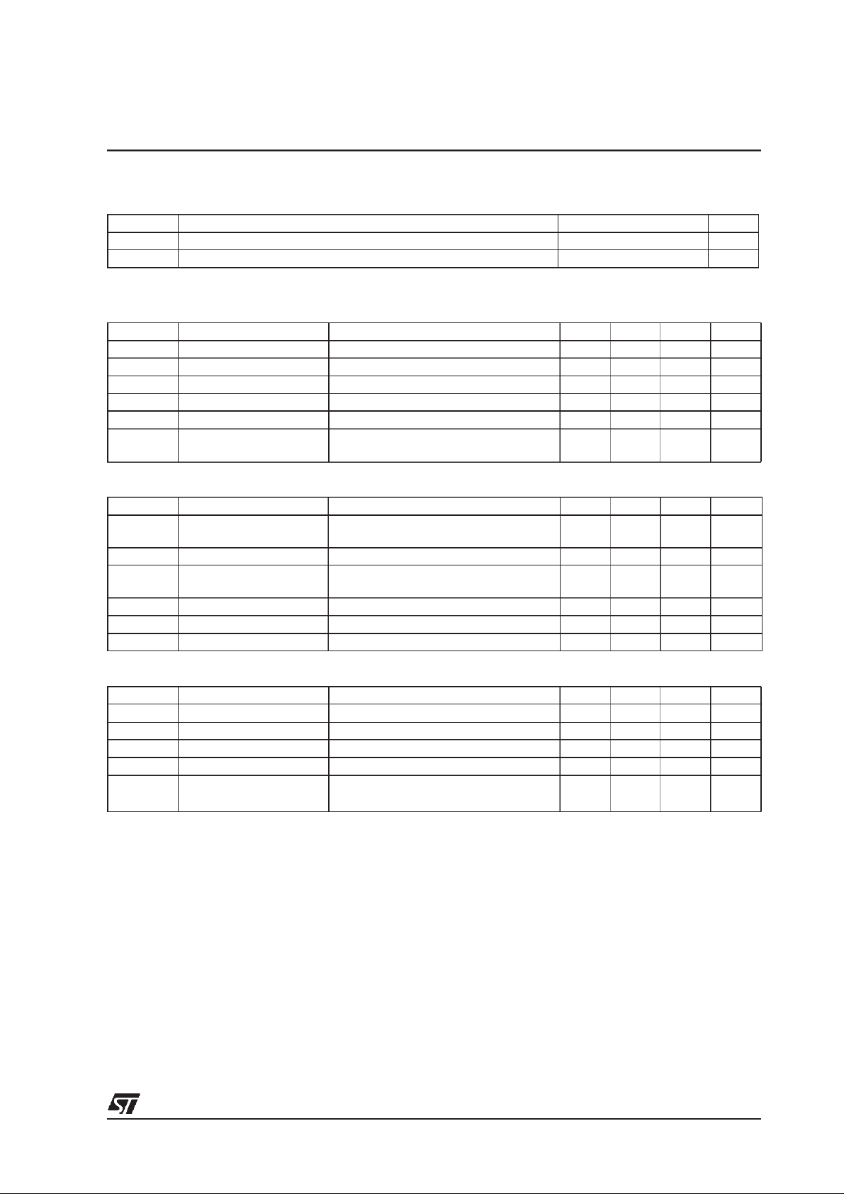
HEPTAWATT
(vertical) (horizontal)
HEPTAWATT
ORDER CODES
HEPTAWATT vertical
HEPTAWATT horizontal
HEPTAWATT in-line
VND05B
VND05B (011Y)
VND05B (012Y)
HEPTAWATT
(in-line)
BLOCK DIAGRAM
(*) In= Nominal current according to ISO definition for high side automotive switch (see note 1)
November 1999 1/11
1
1
VND05B / VND05B (011Y) / VND05B (012Y)
ABSOLUTE MAXIMUM RATING
Symbol Parameter Value Unit
V
(BR)DSS
I
OUT
I
(RMS) RMS Output current at Tc=85°C and f > 1Hz 9 A
OUT
I
R
I
IN
-V
I
STAT
V
ESD
P
TOT
T
T
STG
CONNECTION DIAGRAM TOP VIEW
Drain-Source breakdown voltage 40 V
Output current (continuous) at Tc=85°C9A
Reverse output current at Tc=85°C-9A
Input current +/- 10 mA
Reverse supply voltage -4 V
CC
Status current +/- 10 mA
Electrostatic discharge (R=1.5kΩ, C=100pF) 2000 V
Power dissipation at Tc=25°C59W
Junction operating temperature -40 to 150 °C
j
Storage temperature -55 to 150 °C
CURRENT AND VOLTAGECONVENTIONS
2/11
1
VND05B / VND05B (011Y) / VND05B (012Y)
THERMAL DATA
Symbol Parameter Value Unit
R
thj-case
R
thj-amb
Thermal resistance junction-case (MAX) 2.1 °C/W
Thermal resistance junction-ambient (MAX) 60 °C/W
ELECTRICAL CHARACTERISTICS (8V<VCC<16V; -40°C≤T
≤125°C; unless otherwise specified)
j
POWER
Symbol Parameter Test Conditions Min Typ Max Unit
V
CC
I
n
R
ON
I
V
DS(MAX)
R
S
Supply voltage 6 13 26 V
(*) Nominal current Tc=85°C; V
On state resistance I
OUT=In;VCC
≤0.5V; VCC=13V 1.6 2.6 A
DS(on)
=13V; Tj=25°C 0.13 0.2 Ω
Supply current Off state; Tj=25°C; VCC=13V 35 100 µA
Maximum voltage Drop I
Output to GND internal
i
impedance
=7.5A; Tj=85°C; VCC=13V 1.44 2.3 V
OUT
=25°C 5 10 20 KΩ
T
j
SWITCHING
Symbol Parameter Test Conditions Min Typ Max Unit
t
d(on)
t
(^) Rise time of output current R
r
t
d(off)
t
(^) Fall time of output current R
f
(di/dt)
(di/dt)
Turn-on delay time of
(^)
output current
Turn-off delay time of
(^)
output current
Turn-on current slope R
on
Turn-off current slope R
off
R
=5.4Ω 5 25 200 µs
OUT
=5.4Ω 10 50 180 µs
OUT
R
=5.4Ω 10 75 250 µs
OUT
=5.4Ω 10 35 180 µs
OUT
=5.4Ω 0.003 0.1 A/µs
OUT
=5.4Ω 0.005 0.1 A/µs
OUT
LOGIC INPUT
Symbol Parameter Test Conditions Min Typ Max Unit
V
V
V
I(hyst)
I
IN
V
ICL
Input low level voltage 1.5 V
IL
Input high level voltage 3.5 (•)V
IH
Input hysteresis voltage 0.2 0.9 1.5 V
Input current VIN=5V; Tj=25°C30100µA
Input clamp voltage
=10mA
I
IN
=-10mA
I
IN
56
-0.7
7V
V
3/11
1
VND05B / VND05B (011Y) / VND05B (012Y)
ELECTRICAL CHARACTERISTICS (continued)
PROTECTIONS AND DIAGNOSTICS
Symbol Parameter Test Conditions Min Typ Max Unit
V
STAT
V
USD
V
SCL
T
TSD
T
TSD(hyst)
T
V
OL
I
OL
t
povl
t
pol
(*) In=Nominal current according to ISO definition for high side automotive switch (see note 1)
(^) Seeswitching time waveform
(•)TheV
exceed 10 mA at the input pin.
Note 1: The Nominal Current is the current at T
Note 2: I
Note 3: t
Low output voltage status I
=1.6mA 0.4 V
STAT
Undervoltage shut-down 3.5 4.5 6 V
Status clamp voltage I
Thermal shut-down
temperature
STAT
I
STAT
= 10mA
= -10mA
56
-0.7
140 160 180 °C
Thermal shutdown
hysteresis temperature
Reset temperature 125 °C
R
7V
50 °C
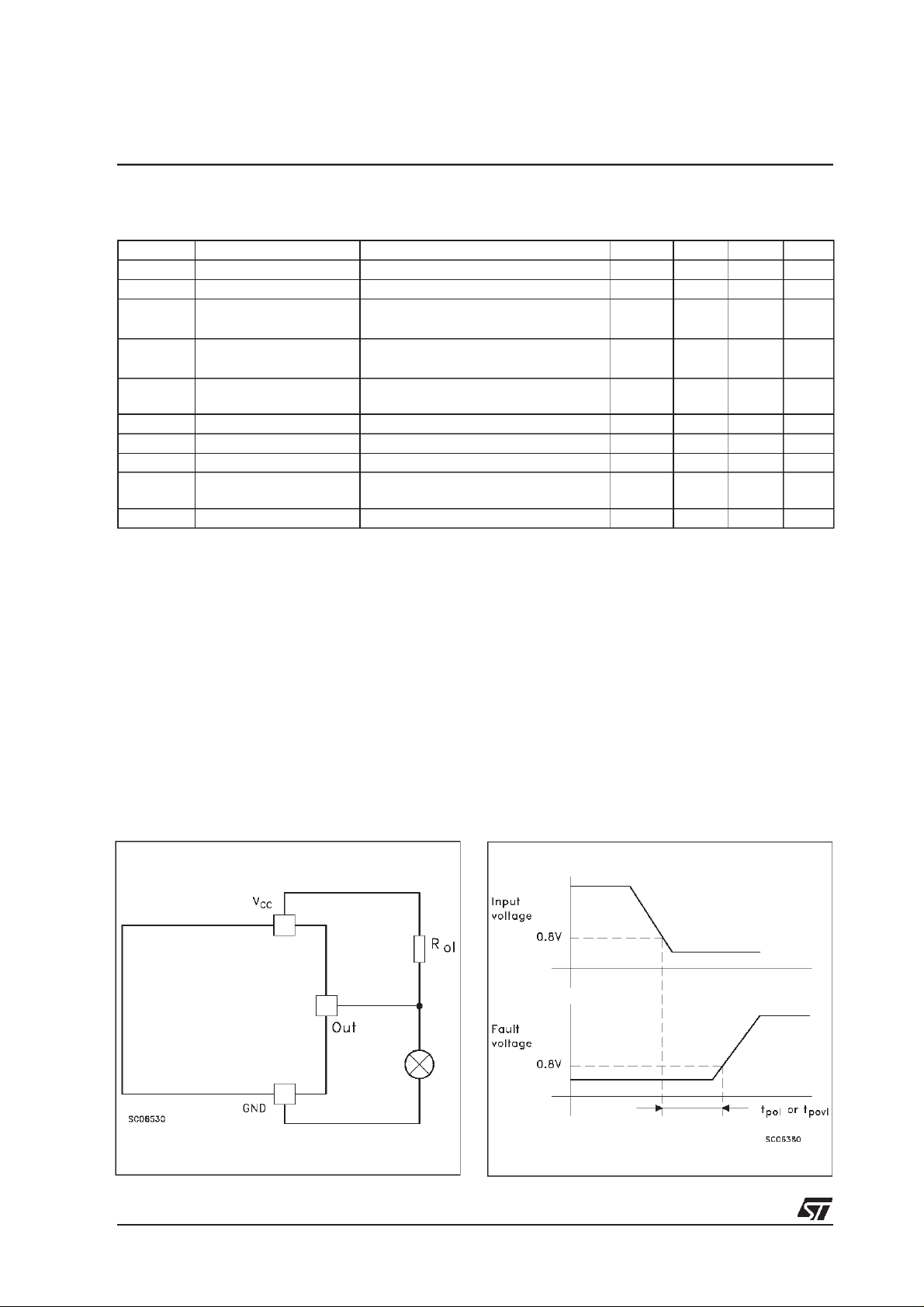
Open voltage level Off state (note 2) 2.5 4 5 V
Open load current level On state 5 180 mA
Overtemperature Status
delay
(note 3) 5 10 µs
Open Load Status delay (note 3) 50 500 2500 µs
is internally clamped at 6V about. It is possible to connect this pin to an higher voltage via an external resistor calculated to not
IH
=85°C for battery voltage of 13V which produces a voltage drop of 0.5V
c
OL(off)
povltpol
=(VCC-VOL)/R
: ISO definition
OL
V
Note 2 Relevant Figure Note 3 Relevant Figure
4/11
2
 Loading...