

Features
Typ e R
VN920SP-E 15 mΩ 30 A 36 V
DS(on)
I
OUT
VN920SP-E
High-side driver
V
CC
■ ECOPACK
■ Automotive Grade: compliance with AEC
®
: lead free and RoHS compliant
guidelines
■ Very low standby current
■ CMOS compatible input
■ Proportional load current sense
■ Current sense disable
■ Thermal shutdown protection and diagnosis
■ Undervoltage shutdown
■ Overvoltage clamp
■ Load current limitation
Description
The VN920SP-E is a monolithic device designed
in STMicroelectronics™ VIPower™ M0-3
technology. The VN920SP-E is intended for
driving any type of load with one side connected
to ground. The active V
protects the device against low energy spikes
(see ISO7637 transient compatibility table).
Active current limitation combined with thermal
shutdown and automatic restart protects the
device against overload.
The device integrates an analog current sense
output which delivers a current proportional to the
load current. The device automatically turns-off in
the case where the ground pin becomes
disconnected.
pin voltage clamp
CC
Table 1. Device summary
Package
PowerSO-10™ VN920SP-E VN920SPTR-E
February 2011 Doc ID 10896 Rev 3 1/27
Order codes
Tube Tape and reel
www.st.com
1

Contents VN920SP-E
Contents
1 Block diagram and pin description . . . . . . . . . . . . . . . . . . . . . . . . . . . . . 5
2 Electrical specifications . . . . . . . . . . . . . . . . . . . . . . . . . . . . . . . . . . . . . . 6
2.1 Absolute maximum ratings . . . . . . . . . . . . . . . . . . . . . . . . . . . . . . . . . . . . . 6
2.2 Thermal data . . . . . . . . . . . . . . . . . . . . . . . . . . . . . . . . . . . . . . . . . . . . . . . 7
2.3 Electrical characteristics . . . . . . . . . . . . . . . . . . . . . . . . . . . . . . . . . . . . . . . 8
2.4 Electrical characteristics curves . . . . . . . . . . . . . . . . . . . . . . . . . . . . . . . . 15
3 Application information . . . . . . . . . . . . . . . . . . . . . . . . . . . . . . . . . . . . . 17
3.1 GND protection network against reverse battery . . . . . . . . . . . . . . . . . . . 17
3.1.1 Solution 1: resistor in the ground line (RGND only) . . . . . . . . . . . . . . . . 17
3.1.2 Solution 2: diode (DGND) in the ground line . . . . . . . . . . . . . . . . . . . . . 18
3.2 Load dump protection . . . . . . . . . . . . . . . . . . . . . . . . . . . . . . . . . . . . . . . . 18
3.3 MCU I/Os protection . . . . . . . . . . . . . . . . . . . . . . . . . . . . . . . . . . . . . . . . . 18
3.4 PowerSO-10 maximum demagnetization energy (V
= 13.5 V) . . . . . . . 19
CC
4 Package and PCB thermal data . . . . . . . . . . . . . . . . . . . . . . . . . . . . . . . 20
4.1 PowerSO-10 thermal data . . . . . . . . . . . . . . . . . . . . . . . . . . . . . . . . . . . . 20
5 Package and packing information . . . . . . . . . . . . . . . . . . . . . . . . . . . . . 23
5.1 ECOPACK® packages . . . . . . . . . . . . . . . . . . . . . . . . . . . . . . . . . . . . . . . 23
5.2 PowerSO-10 mechanical data . . . . . . . . . . . . . . . . . . . . . . . . . . . . . . . . . 23
5.3 PowerSO-10 packing information . . . . . . . . . . . . . . . . . . . . . . . . . . . . . . . 25
6 Revision history . . . . . . . . . . . . . . . . . . . . . . . . . . . . . . . . . . . . . . . . . . . 26
2/27 Doc ID 10896 Rev 3

VN920SP-E List of tables
List of tables
Table 1. Device summary . . . . . . . . . . . . . . . . . . . . . . . . . . . . . . . . . . . . . . . . . . . . . . . . . . . . . . . . . . 1
Table 2. Suggested connections for unused and not connected pins . . . . . . . . . . . . . . . . . . . . . . . . 5
Table 3. Absolute maximum ratings . . . . . . . . . . . . . . . . . . . . . . . . . . . . . . . . . . . . . . . . . . . . . . . . . . 6
Table 4. Thermal data. . . . . . . . . . . . . . . . . . . . . . . . . . . . . . . . . . . . . . . . . . . . . . . . . . . . . . . . . . . . . 7
Table 5. Power . . . . . . . . . . . . . . . . . . . . . . . . . . . . . . . . . . . . . . . . . . . . . . . . . . . . . . . . . . . . . . . . . . 8
Table 6. Switching (V
Table 7. Logic inputs. . . . . . . . . . . . . . . . . . . . . . . . . . . . . . . . . . . . . . . . . . . . . . . . . . . . . . . . . . . . . . 9
Table 8. V
output diode. . . . . . . . . . . . . . . . . . . . . . . . . . . . . . . . . . . . . . . . . . . . . . . . . . . . . . . . . . 9
CC
Table 9. Protections . . . . . . . . . . . . . . . . . . . . . . . . . . . . . . . . . . . . . . . . . . . . . . . . . . . . . . . . . . . . . . 9
Table 10. Current sense . . . . . . . . . . . . . . . . . . . . . . . . . . . . . . . . . . . . . . . . . . . . . . . . . . . . . . . . . . . 10
Table 11. Truth table. . . . . . . . . . . . . . . . . . . . . . . . . . . . . . . . . . . . . . . . . . . . . . . . . . . . . . . . . . . . . . 11
Table 12. Electrical transient requirements on V
Table 13. Electrical transient requirements on V
Table 14. Electrical transient requirements on V
Table 15. Thermal parameters . . . . . . . . . . . . . . . . . . . . . . . . . . . . . . . . . . . . . . . . . . . . . . . . . . . . . . 22
Table 16. PowerSO-10 mechanical data . . . . . . . . . . . . . . . . . . . . . . . . . . . . . . . . . . . . . . . . . . . . . . 24
Table 17. Document revision history . . . . . . . . . . . . . . . . . . . . . . . . . . . . . . . . . . . . . . . . . . . . . . . . . 26
= 13 V) . . . . . . . . . . . . . . . . . . . . . . . . . . . . . . . . . . . . . . . . . . . . . . . . . . . . . 8
CC
pin (part 1) . . . . . . . . . . . . . . . . . . . . . . . . . . . . . 12
CC
pin (part 2) . . . . . . . . . . . . . . . . . . . . . . . . . . . . . 12
CC
pin (part 3) . . . . . . . . . . . . . . . . . . . . . . . . . . . . . 12
CC
Doc ID 10896 Rev 3 3/27

List of figures VN920SP-E
List of figures
Figure 1. Block diagram . . . . . . . . . . . . . . . . . . . . . . . . . . . . . . . . . . . . . . . . . . . . . . . . . . . . . . . . . . . . 5
Figure 2. Configuration diagram (top view) . . . . . . . . . . . . . . . . . . . . . . . . . . . . . . . . . . . . . . . . . . . . . 5
Figure 3. Current and voltage conventions . . . . . . . . . . . . . . . . . . . . . . . . . . . . . . . . . . . . . . . . . . . . . 6
Figure 4. Switching characteristics (resistive load R
Figure 5. I
OUT/ISENSE
versus I
. . . . . . . . . . . . . . . . . . . . . . . . . . . . . . . . . . . . . . . . . . . . . . . . . . . 13
OUT
Figure 6. Waveforms . . . . . . . . . . . . . . . . . . . . . . . . . . . . . . . . . . . . . . . . . . . . . . . . . . . . . . . . . . . . . 14
Figure 7. Off-state output current . . . . . . . . . . . . . . . . . . . . . . . . . . . . . . . . . . . . . . . . . . . . . . . . . . . . 15
Figure 8. High level input current . . . . . . . . . . . . . . . . . . . . . . . . . . . . . . . . . . . . . . . . . . . . . . . . . . . . 15
Figure 9. Input clamp voltage. . . . . . . . . . . . . . . . . . . . . . . . . . . . . . . . . . . . . . . . . . . . . . . . . . . . . . . 15
Figure 10. On-state resistance vs V
Figure 11. On-state resistance vs T
. . . . . . . . . . . . . . . . . . . . . . . . . . . . . . . . . . . . . . . . . . . . . . . . . 15
CC
. . . . . . . . . . . . . . . . . . . . . . . . . . . . . . . . . . . . . . . . . . . . . . . . 15
case
Figure 12. Input high level . . . . . . . . . . . . . . . . . . . . . . . . . . . . . . . . . . . . . . . . . . . . . . . . . . . . . . . . . . 15
Figure 13. Input low level . . . . . . . . . . . . . . . . . . . . . . . . . . . . . . . . . . . . . . . . . . . . . . . . . . . . . . . . . . . 16
Figure 14. Input hysteresis voltage . . . . . . . . . . . . . . . . . . . . . . . . . . . . . . . . . . . . . . . . . . . . . . . . . . . 16
Figure 15. Turn-on voltage slope . . . . . . . . . . . . . . . . . . . . . . . . . . . . . . . . . . . . . . . . . . . . . . . . . . . . . 16
Figure 16. Turn-off voltage slope . . . . . . . . . . . . . . . . . . . . . . . . . . . . . . . . . . . . . . . . . . . . . . . . . . . . . 16
Figure 17. Overvoltage shutdown . . . . . . . . . . . . . . . . . . . . . . . . . . . . . . . . . . . . . . . . . . . . . . . . . . . . 16
Figure 18. I
LIM
vs T
. . . . . . . . . . . . . . . . . . . . . . . . . . . . . . . . . . . . . . . . . . . . . . . . . . . . . . . . . . . . 16
case
Figure 19. Application schematic . . . . . . . . . . . . . . . . . . . . . . . . . . . . . . . . . . . . . . . . . . . . . . . . . . . . . 17
Figure 20. PowerSO-10 maximum turn-off current versus inductance . . . . . . . . . . . . . . . . . . . . . . . . 19
Figure 21. PowerSO-10 PC board . . . . . . . . . . . . . . . . . . . . . . . . . . . . . . . . . . . . . . . . . . . . . . . . . . . . 20
Figure 22. R
vs PCB copper area in open box free air condition . . . . . . . . . . . . . . . . . . . . . . . 20
thj-amb
Figure 23. PowerSO-10 thermal impedance junction ambient single pulse . . . . . . . . . . . . . . . . . . . . 21
Figure 24. Thermal fitting model of a single channel HSD in PowerSO-10 . . . . . . . . . . . . . . . . . . . . . 21
Figure 25. PowerSO-10 package dimensions . . . . . . . . . . . . . . . . . . . . . . . . . . . . . . . . . . . . . . . . . . . 23
Figure 26. PowerSO-10 suggested pad layout and tube shipment (no suffix) . . . . . . . . . . . . . . . . . . 25
Figure 27. PowerSO-10 tape and reel shipment (suffix “TR”) . . . . . . . . . . . . . . . . . . . . . . . . . . . . . . . 25
=1.3Ω) . . . . . . . . . . . . . . . . . . . . . . . . . . . . . . 13
L
4/27 Doc ID 10896 Rev 3
VN920SP-E Block diagram and pin description
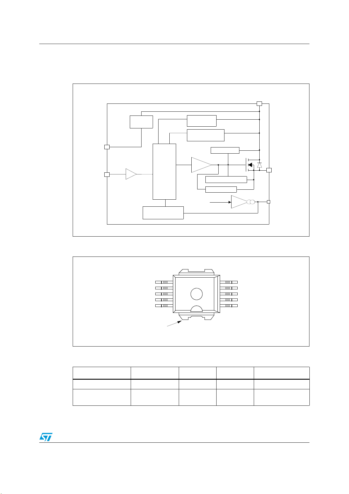
1 Block diagram and pin description
Figure 1. Block diagram
V
CC
V
CC
CLAMP
GND
INPUT
LOGIC
OVERTEMPERATURE
DETECTION
OVERVOLTAGE
DETECTION
UNDERVOLTAGE
DRIVER
Figure 2. Configuration diagram (top view)
GROUND
INPUT
C.SENSE
N.C.
N.C.
6
7
8
9
10
V
CC
11
DETECTION
Power CLAMP
CURRENT LIMITER
VDS LIMITER
I
OUT CURRENT
5
4
3
2
1
K
OUTPUT
OUTPUT
N.C.
OUTPUT
OUTPUT
OUTPUT
SENSE
PowerSO-10
Table 2. Suggested connections for unused and not connected pins
Connection / pin Current sense N.C. Output Input
Floating X X X
To ground
Through 1 KΩ
resistor
X
Through 10KΩ
Doc ID 10896 Rev 3 5/27
resistor

Electrical specifications VN920SP-E
2 Electrical specifications
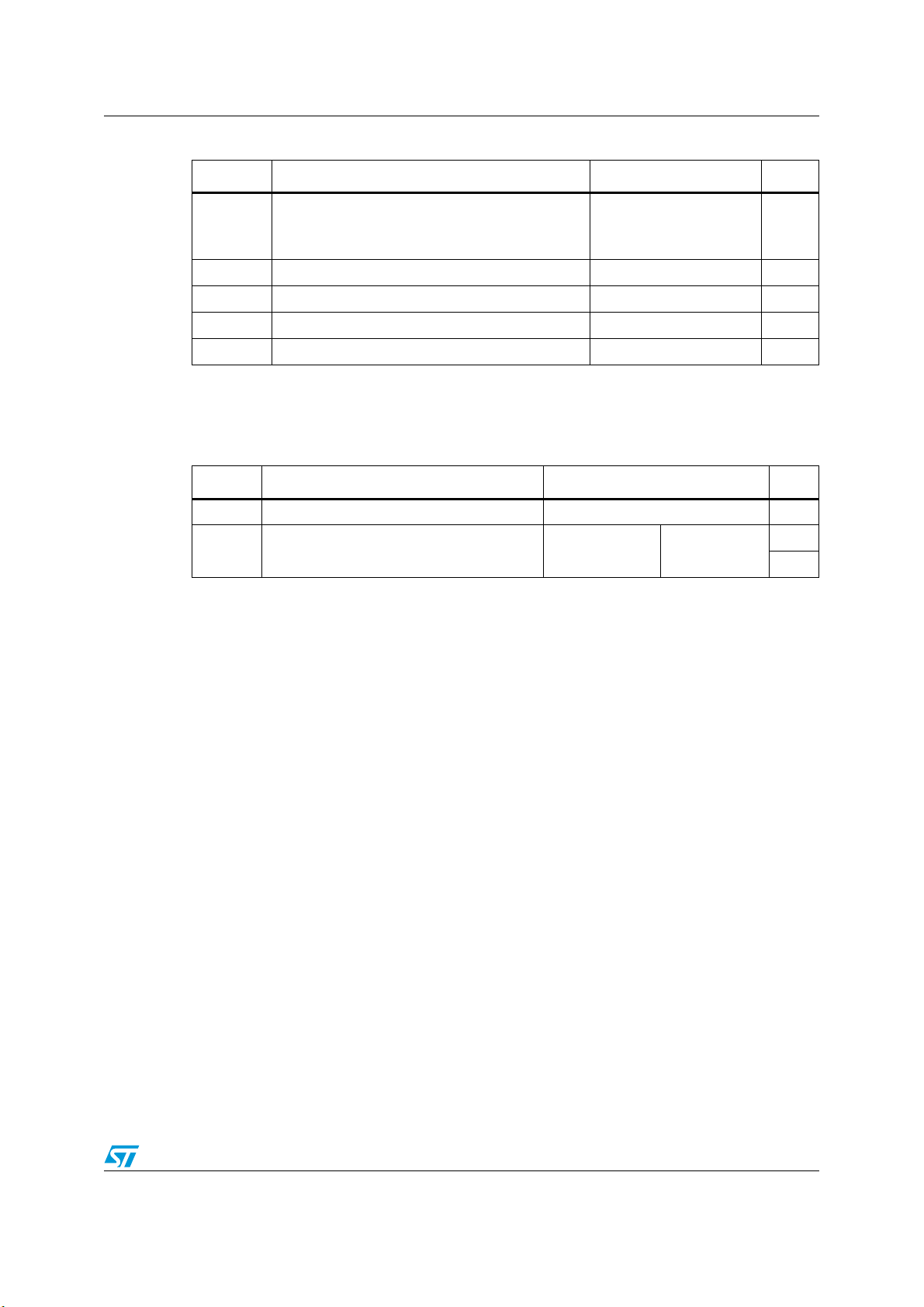
Figure 3. Current and voltage conventions
I
S
V
CC
I
OUT
I
SENSE
V
SENSE
GND
OUTPUT
I
GND
I
IN
V
IN
INPUT
CURRENT SENSE
V
F
V
OUT
V
CC
2.1 Absolute maximum ratings
Stressing the device above the rating listed in Ta bl e 3 may cause permanent damage to the
device. These are stress ratings only and operation of the device at these or any other
conditions above those indicated in the operating sections of this specification is not implied.
Exposure to absolute maximum rating conditions for extended periods may affect device
reliability. Refer also to the STMicroelectronics sure program and other relevant quality
document.
Table 3. Absolute maximum ratings
Symbol Parameter Value Unit
V
- V
- I
GND
I
OUT
- I
OUT
I
V
CSENSE
V
ESD
CC
IN
DC supply voltage 41 V
Reverse DC supply voltage -0.3 V
CC
DC reverse ground pin current -200 mA
DC output current Internally limited A
Reverse DC output current -40 A
DC input current +/-10 mA
Current sense maximum voltage
Electrostatic discharge
(Human Body Model: R = 1.5 KΩ; C = 100 pF)
– INPUT
– CURRENT SENSE
–OUTPUT
–V
CC
-3
+15
4000
2000
5000
5000
V
V
V
V
V
V
6/27 Doc ID 10896 Rev 3
VN920SP-E Electrical specifications
Table 3. Absolute maximum ratings (continued)
Symbol Parameter Value Unit
Maximum switching energy
E
T
MAX
P
T
T
STG
(L = 0.25 mH; R
= 150 °C; IL = 45 A)
T
jstart
Power dissipation TC ≤ 25 °C 96.1 W
tot
Junction operating temperature Internally limited °C
j
Case operating temperature -40 to 150 °C
c
= 0 Ω; V
L
= 13.5 V;
bat
Storage temperature -55 to 150 °C
362 mJ
2.2 Thermal data
Table 4. Thermal data
Symbol Parameter Max. value Unit
R
thj-case
R
thj-amb
1. When mounted on FR4 printed circuit board with 0.5 cm2 of Cu (at least 35 µm thick).
2. When mounted on FR4 printed circuit board with 6 cm2 of Cu (at least 35 µm thick).
Thermal resistance junction-case (max) 1.3 °C/W
Thermal resistance junction-ambient (max) 51.3
(1)
37
(2)
°C/W
°C/W
Doc ID 10896 Rev 3 7/27
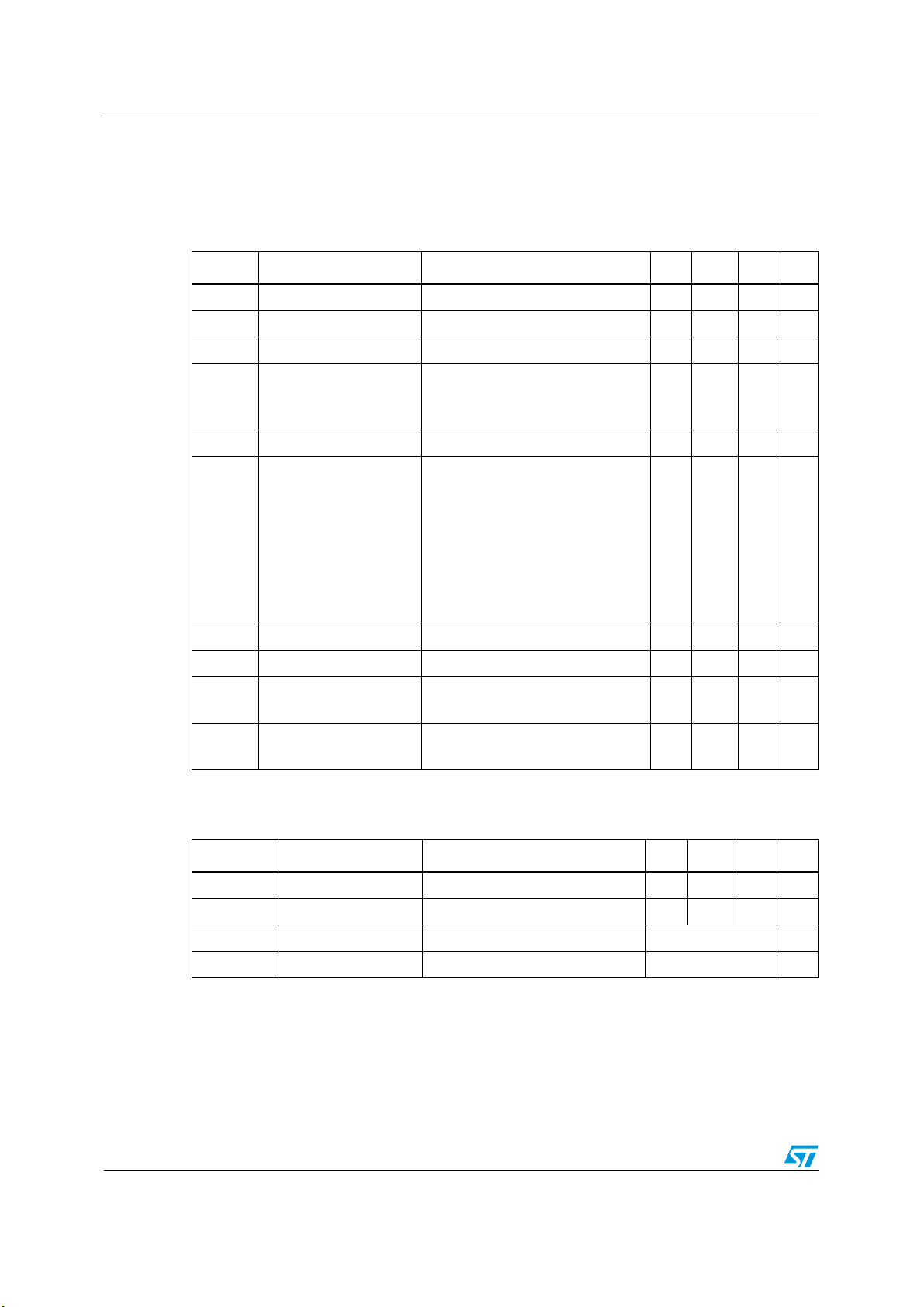
Electrical specifications VN920SP-E
2.3 Electrical characteristics
Values specified in this section are for 8 V < V
< 36 V; -40 °C < Tj < 150 °C, unless
CC
otherwise stated.
Tabl e 5. Pow er
Symbol Parameter Test conditions Min. Typ. Max. Unit
V
V
V
R
V
CLAMP
I
L(off1)
I
L(off2)
I
L(off3)
Operating supply voltage 5.5 13 36 V
CC
Undervoltage shutdown 3 4 5.5 V
USD
Overvoltage shutdown 36 V
OV
I
= 10 A; Tj = 25 °C;
OUT
On-state resistance
ON
Clamp voltage I
Supply current
I
S
Off-state output current V
Off-state output current V
Off-state output current
I
= 10 A;
OUT
= 3 A; V
I
OUT
= 20 mA
CC
Off-state; V
= V
V
IN
OUT
Off-state; V
= V
V
IN
OUT
On-state; V
= 0 A; R
I
OUT
= V
IN
OUT
= 0 V; V
IN
V
= V
IN
OUT
Tj = 125 °C
= 6 V
CC
(1)
CC
= 13 V;
41 48 55 V
= 0 V
= 13 V;
CC
= 0 V; Tj = 25 °C
= 13 V; V
CC
SENSE
= 5 V;
IN
= 3.9 kΩ
= 0 V 0 50 µA
= 3.5 V -75 0 µA
OUT
= 0 V; V
CC
= 13 V;
15
30
50
101025
20
5
5µA
mΩ
mΩ
mΩ
µA
µA
mA
V
I
L(off4)
1. V
Table 6. Switching (VCC=13V)
Off-state output current
and VOV are correlated. Typical difference is 5 V.
CLAMP
IN
Tj = 25 °C
= V
OUT
= 0 V; V
Symbol Parameter Test conditions Min. Typ. Max. Unit
dV
dV
t
d(on)
t
d(off)
OUT
OUT
Turn-on delay time RL = 1.3 Ω (see Figure 4)50µs
Turn-off delay time RL = 1.3 Ω (see Figure 4)50µs
/dt
Turn-on voltage slope RL = 1.3 Ω (see Figure 4) See Figure 15 V/µs
(on)
/dt
Turn-off voltage slope RL = 1.3 Ω (see Figure 4) See Figure 16 V/µs
(off)
8/27 Doc ID 10896 Rev 3
CC
= 13 V;
3µA
VN920SP-E Electrical specifications
Table 7. Logic inputs
Symbol Parameter Test conditions Min. Typ. Max. Unit
V
V
V
I(hyst)
V
Tabl e 8. VCC output diode
Input low level voltage 1.25 V
IL
Low level input current V
I
IL
Input high level voltage 3.25 V
IH
I
High level input current V
IH
= 1.25 V 1 µA
IN
= 3.25 V 10 µA
IN
Input hysteresis voltage 0.5 V
Input clamp voltage
ICL
I
= 1 mA
IN
= - 1 mA
I
IN
66.8
-0.7
8V
Symbol Parameter Test conditions Min. Typ. Max. Unit
V
F
Table 9. Protections
Forward on voltage - I
(1)
= 5.3 A; Tj = 150 °C - - 0.6 V
OUT
Symbol Parameter Test conditions Min. Typ. Max. Unit
T
TSD
T
T
hyst
I
lim
V
demag
V
1. To ensure long term reliability under heavy over-load or short circuit conditions, protection and related
diagnostic signals must be used together with a proper software strategy. If the device operates under
abnormal conditions this software must limit the duration and number of activation cycles.
Shutdown temperature 150 175 200 °C
Reset temperature 135 °C
R
Thermal hysteresis 7 15 °C
DC short circuit current
Turn-off output clamp
voltage
Output voltage drop
ON
limitation
V
= 13 V
CC
5V < V
I
OUT
V
IN
CC
= 2 A;
= 0 V;
< 36 V
L = 6 mH
= 1 A;
I
OUT
= -40 °C...150 °C
T
j
30 45 75
V
CC
- 41 V
CC
- 48 V
50 mV
75
- 55 V
CC
V
A
A
Doc ID 10896 Rev 3 9/27
 Loading...