

ST VN920PEP-E User Manual
Features
Typ e R
DS(on)
VN920PEP-E 15 mΩ 30 A 36 V
■ CMOS compatible input
■ Proportional load current sense
■ Shorted load protection
■ Under voltage and overvoltage shutdown
■ Overvoltage clamp
■ Thermal shutdown
■ Current limitation
■ Protection against loss of ground and loss of
V
CC
■
Very low standby power dissipation
■ Reverse battery protected (see Application
schematic on page 17)
■ In compliance with the 2002/95/ec european
directive
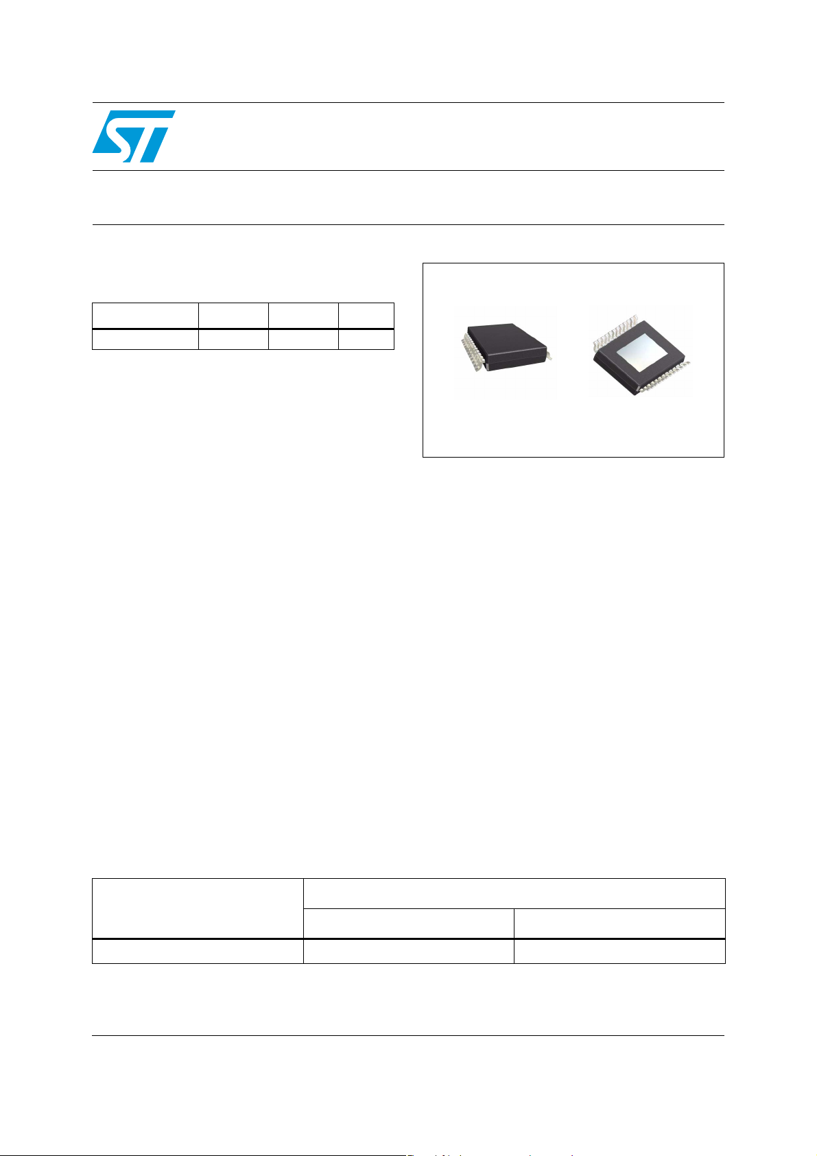
Table 1. Device summary
I
OUT
V
CC
VN920PEP-E
Single channel high side driver
PowerSSO-24
Description
The VN920PEP-E is a monolithic device designed
in STMicroelectronics VIPower™ M0-3
technology, intended for driving any kind of load
with one side connected to ground. Active V
voltage clamp protects the device against low
energy spikes (see ISO7637 transient
compatibility able).
Active current limitation combined with thermal
shutdown and automatic restart protect the device
against overload. The device integrates an analog
current sense output which delivers a current
proportional to the load current. Device
automatically turns off in case of ground pin
disconnection.
CC
pin
Order codes
Package
Tube Tape and reel
PowerSSO-24 VN920PEP-E VN920PEPTR-E
July 2009 Doc ID 10874 Rev 6 1/26
www.st.com
1

Contents VN920PEP-E
Contents
1 Block diagram and pin description . . . . . . . . . . . . . . . . . . . . . . . . . . . . . 5
2 Electrical specifications . . . . . . . . . . . . . . . . . . . . . . . . . . . . . . . . . . . . . . 6
2.1 Absolute maximum ratings . . . . . . . . . . . . . . . . . . . . . . . . . . . . . . . . . . . . . 6
2.2 Thermal data . . . . . . . . . . . . . . . . . . . . . . . . . . . . . . . . . . . . . . . . . . . . . . . 7
2.3 Electrical characteristics . . . . . . . . . . . . . . . . . . . . . . . . . . . . . . . . . . . . . . . 7
2.4 Electrical characteristics curves . . . . . . . . . . . . . . . . . . . . . . . . . . . . . . . . 15
3 Application information . . . . . . . . . . . . . . . . . . . . . . . . . . . . . . . . . . . . . 17
3.1 GND protection network against reverse battery . . . . . . . . . . . . . . . . . . . 17
3.1.1 Solution 1: resistor in the ground line (RGND only) . . . . . . . . . . . . . . . . 17
3.1.2 Solution 2: diode (DGND) in the ground line . . . . . . . . . . . . . . . . . . . . . 18
3.2 Load dump protection . . . . . . . . . . . . . . . . . . . . . . . . . . . . . . . . . . . . . . . . 18
3.3 MCU I/Os protection . . . . . . . . . . . . . . . . . . . . . . . . . . . . . . . . . . . . . . . . . 18
3.4 PowerSSO-24 maximum demagnetization energy (V
=13.5V) . . . . . . . 19
CC
4 Package and PCB thermal data . . . . . . . . . . . . . . . . . . . . . . . . . . . . . . . 20
4.1 PowerSSO-24 thermal data . . . . . . . . . . . . . . . . . . . . . . . . . . . . . . . . . . . 20
5 Package and packing information . . . . . . . . . . . . . . . . . . . . . . . . . . . . . 23
5.1 ECOPACK® packages . . . . . . . . . . . . . . . . . . . . . . . . . . . . . . . . . . . . . . . 23
6 Revision history . . . . . . . . . . . . . . . . . . . . . . . . . . . . . . . . . . . . . . . . . . . 25
2/26 Doc ID 10874 Rev 6

VN920PEP-E List of tables
List of tables
Table 1. Device summary . . . . . . . . . . . . . . . . . . . . . . . . . . . . . . . . . . . . . . . . . . . . . . . . . . . . . . . . . . 1
Table 2. Suggested connections for unused and not connected pins . . . . . . . . . . . . . . . . . . . . . . . . 5
Table 3. Absolute maximum ratings . . . . . . . . . . . . . . . . . . . . . . . . . . . . . . . . . . . . . . . . . . . . . . . . . . 6
Table 4. Thermal data. . . . . . . . . . . . . . . . . . . . . . . . . . . . . . . . . . . . . . . . . . . . . . . . . . . . . . . . . . . . . 7
Table 5. Power . . . . . . . . . . . . . . . . . . . . . . . . . . . . . . . . . . . . . . . . . . . . . . . . . . . . . . . . . . . . . . . . . . 7
Table 6. Switching (V
Table 7. Logic inputs. . . . . . . . . . . . . . . . . . . . . . . . . . . . . . . . . . . . . . . . . . . . . . . . . . . . . . . . . . . . . . 8
Table 8. Current sense (9V £ VCC £ 16V) . . . . . . . . . . . . . . . . . . . . . . . . . . . . . . . . . . . . . . . . . . . . . 9
Table 9. Protections . . . . . . . . . . . . . . . . . . . . . . . . . . . . . . . . . . . . . . . . . . . . . . . . . . . . . . . . . . . . . . 9
Table 10. V
output diode. . . . . . . . . . . . . . . . . . . . . . . . . . . . . . . . . . . . . . . . . . . . . . . . . . . . . . . . . 10
CC
Table 11. Truth table. . . . . . . . . . . . . . . . . . . . . . . . . . . . . . . . . . . . . . . . . . . . . . . . . . . . . . . . . . . . . . 11
Table 12. Electrical transient requirements (part 1/3). . . . . . . . . . . . . . . . . . . . . . . . . . . . . . . . . . . . . 12
Table 13. Electrical transient requirements (part 2/3). . . . . . . . . . . . . . . . . . . . . . . . . . . . . . . . . . . . . 12
Table 14. Electrical transient requirements (part 3/3). . . . . . . . . . . . . . . . . . . . . . . . . . . . . . . . . . . . . 13
Table 15. PowerSSO-24 thermal parameters. . . . . . . . . . . . . . . . . . . . . . . . . . . . . . . . . . . . . . . . . . . 21
Table 16. PowerSSO-24™ mechanical data . . . . . . . . . . . . . . . . . . . . . . . . . . . . . . . . . . . . . . . . . . . 23
Table 17. Document revision history . . . . . . . . . . . . . . . . . . . . . . . . . . . . . . . . . . . . . . . . . . . . . . . . . 25
=13V) . . . . . . . . . . . . . . . . . . . . . . . . . . . . . . . . . . . . . . . . . . . . . . . . . . . . . . 8
CC
Doc ID 10874 Rev 6 3/26

List of figures VN920PEP-E
List of figures
Figure 1. Block diagram . . . . . . . . . . . . . . . . . . . . . . . . . . . . . . . . . . . . . . . . . . . . . . . . . . . . . . . . . . . . 5
Figure 2. Configuration diagram (top view) . . . . . . . . . . . . . . . . . . . . . . . . . . . . . . . . . . . . . . . . . . . . . 5
Figure 3. Current and voltage conventions . . . . . . . . . . . . . . . . . . . . . . . . . . . . . . . . . . . . . . . . . . . . . 6
Figure 4. I
OUT/ISENSE
Figure 5. Switching characteristics . . . . . . . . . . . . . . . . . . . . . . . . . . . . . . . . . . . . . . . . . . . . . . . . . . 11
Figure 6. Switching time waveforms . . . . . . . . . . . . . . . . . . . . . . . . . . . . . . . . . . . . . . . . . . . . . . . . . 12
Figure 7. Waveforms . . . . . . . . . . . . . . . . . . . . . . . . . . . . . . . . . . . . . . . . . . . . . . . . . . . . . . . . . . . . . 14
Figure 8. Off-state output current . . . . . . . . . . . . . . . . . . . . . . . . . . . . . . . . . . . . . . . . . . . . . . . . . . . . 15
Figure 9. High level input current . . . . . . . . . . . . . . . . . . . . . . . . . . . . . . . . . . . . . . . . . . . . . . . . . . . . 15
Figure 10. Input clamp voltage. . . . . . . . . . . . . . . . . . . . . . . . . . . . . . . . . . . . . . . . . . . . . . . . . . . . . . . 15
Figure 11. Input high level voltage . . . . . . . . . . . . . . . . . . . . . . . . . . . . . . . . . . . . . . . . . . . . . . . . . . . . 15
Figure 12. Input low level voltage . . . . . . . . . . . . . . . . . . . . . . . . . . . . . . . . . . . . . . . . . . . . . . . . . . . . 15
Figure 13. Input hysteresis voltage . . . . . . . . . . . . . . . . . . . . . . . . . . . . . . . . . . . . . . . . . . . . . . . . . . . 15
Figure 14. Overvoltage shutdown . . . . . . . . . . . . . . . . . . . . . . . . . . . . . . . . . . . . . . . . . . . . . . . . . . . . 16
Figure 15. ILIM vs Tcase . . . . . . . . . . . . . . . . . . . . . . . . . . . . . . . . . . . . . . . . . . . . . . . . . . . . . . . . . . . 16
Figure 16. Turn-on voltage slope . . . . . . . . . . . . . . . . . . . . . . . . . . . . . . . . . . . . . . . . . . . . . . . . . . . . . 16
Figure 17. Turn-off voltage slope . . . . . . . . . . . . . . . . . . . . . . . . . . . . . . . . . . . . . . . . . . . . . . . . . . . . . 16
Figure 18. On-state resistance vs T
Figure 19. Application schematic . . . . . . . . . . . . . . . . . . . . . . . . . . . . . . . . . . . . . . . . . . . . . . . . . . . . . 17
Figure 20. PowerSSO-24 maximum turn-off current versus inductance . . . . . . . . . . . . . . . . . . . . . . . 19
Figure 21. PowerSSO-24 PC board. . . . . . . . . . . . . . . . . . . . . . . . . . . . . . . . . . . . . . . . . . . . . . . . . . . 20
Figure 22. PowerSSO-24 Rthj-amb vs PCB copper area in open box free air condition . . . . . . . . . . 20
Figure 23. PowerSSO-24 thermal impedance junction ambient single pulse . . . . . . . . . . . . . . . . . . . 21
Figure 24. Thermal fitting model of a single channel HSD in PowerSSO-24 . . . . . . . . . . . . . . . . . . . . 21
Figure 25. PowerSSO-24 package dimensions . . . . . . . . . . . . . . . . . . . . . . . . . . . . . . . . . . . . . . . . . . 23
versus I
. . . . . . . . . . . . . . . . . . . . . . . . . . . . . . . . . . . . . . . . . . . . . . . . . . . 10
OUT
. . . . . . . . . . . . . . . . . . . . . . . . . . . . . . . . . . . . . . . . . . . . . . . 16
CASE
4/26 Doc ID 10874 Rev 6
VN920PEP-E Block diagram and pin description
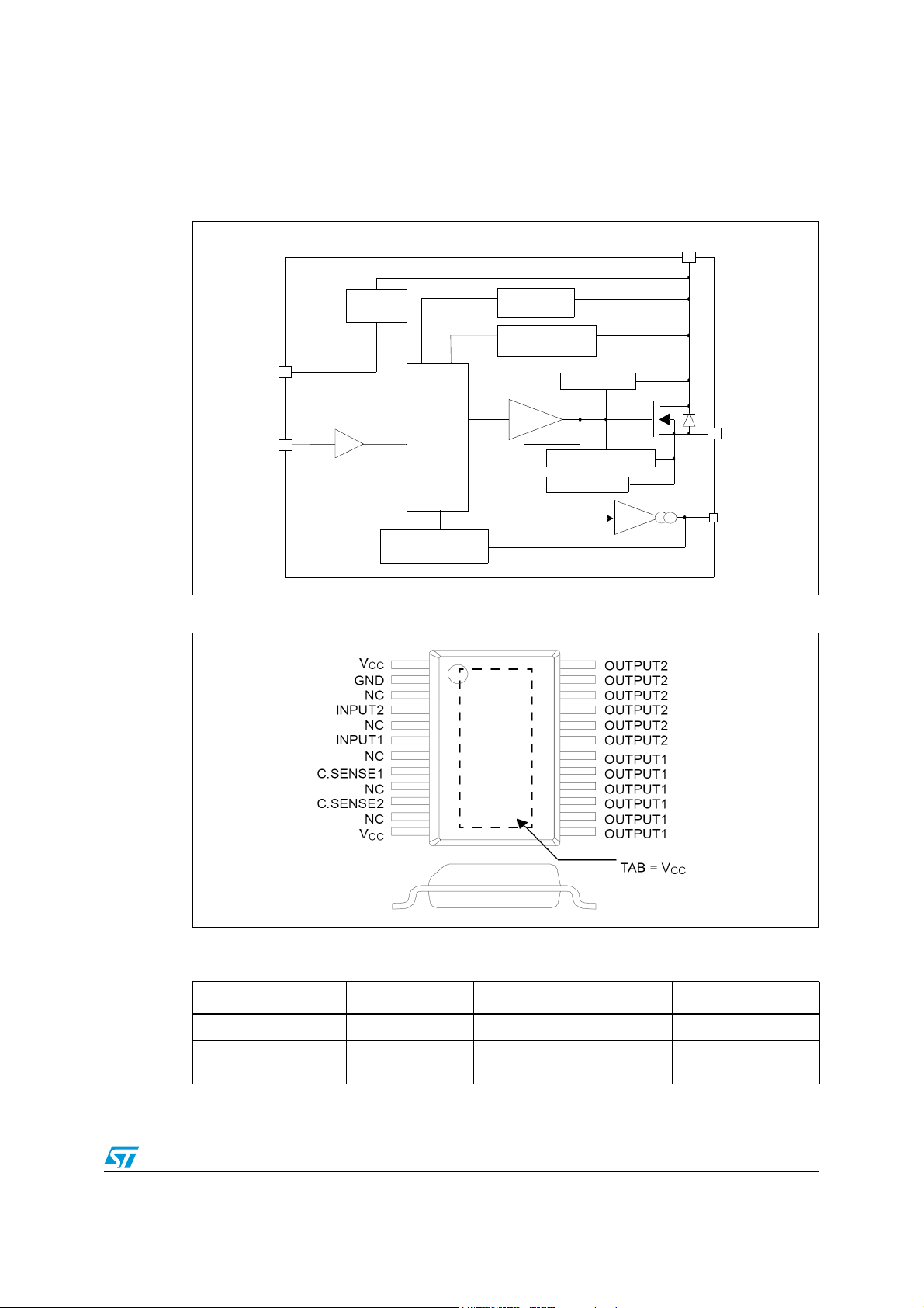
1 Block diagram and pin description
Figure 1. Block diagram
V
CC
V
CC
CLAMP
OVERVOLTAGE
DETECTION
UNDERVOLTAGE
GND
INPUT
LOGIC
OVERTEMPERATURE
DETECTION
Figure 2. Configuration diagram (top view)
DETECTION
DRIVER
Power CLAMP
OUTPUT
CURRENT LIMITER
VDS LIMITER
I
OUT CURRENT
K
SENSE
Table 2. Suggested connections for unused and not connected pins
Connection / pin Current Sense N.C. Output Input
Floating X X X
To ground
Through 1KΩ
resistor
X
Through 10KΩ
resistor
Doc ID 10874 Rev 6 5/26
Electrical specifications VN920PEP-E
2 Electrical specifications
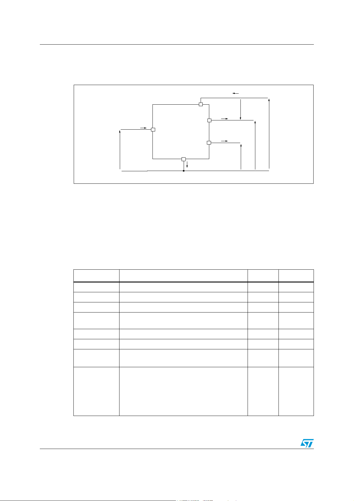
Figure 3. Current and voltage conventions
I
S
V
I
IN
V
IN
INPUT
CURRENT SENSE
2.1 Absolute maximum ratings
GND
CC
OUTPUT
I
GND
I
OUT
I
SENSE
V
SENSE
V
F
V
OUT
V
CC
Stressing the device above the rating listed in the “Absolute maximum ratings” table may
cause permanent damage to the device. These are stress ratings only and operation of the
device at these or any other conditions above those indicated in the operating sections of
this specification is not implied. Exposure to Absolute maximum rating conditions for
extended periods may affect device reliability. Refer also to the STMicroelectronics sure
program and other relevant quality document.
Table 3. Absolute maximum ratings
Symbol Parameter Value Unit
V
CC
- V
CC
- I
gnd
I
OUT
- I
OUT
I
IN
V
CSENSE
V
ESD
DC supply voltage 41 V
Reverse DC supply voltage - 0.3 V
DC reverse ground pin current - 200 mA
DC output current
Internally
limited
A
Reverse DC output current - 40 A
DC input current +/- 10 mA
Current sense maximum voltage
- 3
+ 15
V
V
Electrostatic discharge
(human body model: R = 1.5KΩ; C = 100pF)
– Input
– Current sense
– Output
–V
CC
4000
2000
5000
5000
V
V
V
V
6/26 Doc ID 10874 Rev 6
VN920PEP-E Electrical specifications
Table 3. Absolute maximum ratings (continued)
Symbol Parameter Value Unit
Maximum switching energy
E
MAX
P
T
T
T
stg
(L = 0.3mH; R
= 45A)
I
L
tot
j
c
Power dissipation TC ≤ 25°C 8.3 W
Junction operating temperature
Case operating temperature - 40 to 150 °C
= 0Ω; V
L
= 13.5V; T
bat
jstart
= 150°C;
Storage temperature - 55 to 150 °C
462 mJ
Internally
limited
°C
2.2 Thermal data
Table 4. Thermal data
Symbol Parameter Max. value Unit
R
thj-case
R
thj-amb
Thermal resistance junction-case (max) 1.3 °C/W
Thermal resistance junction-ambient (max) 55
1. When mounted on a standard single-sided FR-4 board with 0.5cm2 of Cu (at least 35µm thick).
2. When mounted on a standard single-sided FR-4 board with 8cm2 of Cu (at least 35ɵm thick).
2.3 Electrical characteristics
Values specified in this section are for 8V < V
stated.
Table 5. Power
Symbol Parameter Test conditions Min. Typ. Max. Unit
V
V
V
R
V
CLAMP
Operating supply voltage 5.5 13 36 V
CC
Undervoltage shutdown 3 4 5.5 V
USD
Overvoltage shutdown 36 V
OV
I
OUT
On-state resistance
ON
Clamp voltage I
I
OUT
I
OUT
CC
< 36V; -40°C < Tj < 150°C, unless otherwise
CC
= 10A; Tj = 25°C;
= 10A;
= 3A; V
= 20mA
(1)
CC
= 6V
(1)
(2)
40
°C/W
41 48 55 V
15
30
50
mΩ
mΩ
mΩ
Doc ID 10874 Rev 6 7/26
Electrical specifications VN920PEP-E
Table 5. Power (continued)
Symbol Parameter Test conditions Min. Typ. Max. Unit
I
Supply current
S
I
L(off1)
I
L(off3)
I
L(off4)
1. V
Table 6. Switching (VCC=13V)
Off-state output current V
Off-state output current
Off-state output current
and VOV are correlated. Typical difference is 5V.
clamp
Off-state; V
V
= V
IN
Off-state; V
V
= V
IN
On-state; V
I
= 0A; R
OUT
= V
IN
V
= V
IN
V
= 13V; Tj = 125°C
CC
V
= V
IN
V
= 13V; Tj = 25°C
CC
= 13V;
CC
= 0V
OUT
= 13V;
CC
= 0V; Tj = 25°C
OUT
= 13V; V
CC
SENSE
= V
OUT
OUT
OUT
= V
= V
SENSE
SENSE
SENSE
101025
20
= 5V;
IN
= 3.9 kΩ
5
= 0V 0 50 µA
= 0V;
= 0V;
5µA
3µA
Symbol Parameter Test conditions Min. Typ. Max. Unit
dV
dV
t
d(on)
t
d(off)
OUT
OUT
Turn-on delay time RL = 1.3Ω (see Figure 5)50µs
Turn-off delay time RL = 1.3Ω (see Figure 5)50µs
/dt
Turn-on voltage slope RL = 1.3Ω (see Figure 5) See Figure 16 V/µs
(on)
/dt
Turn-off voltage slope RL = 1.3Ω (see Figure 5) See Figure 17 V/µs
(off)
µA
µA
mA
Table 7. Logic inputs
Symbol Parameter Test conditions Min. Typ. Max. Unit
V
V
V
I(hyst)
V
Input low level voltage 1.25 V
IL
Low level input current V
I
IL
Input high-level voltage 3.25 V
IH
I
High-level input current V
IH
Input hysteresis voltage 0.5 V
Input clamp voltage
ICL
8/26 Doc ID 10874 Rev 6
= 1.25V 1 µA
IN
= 3.25V 10 µA
IN
I
IN
I
IN
= 1mA
= - 1mA
66.8
- 0.7
8V
V
 Loading...