

Features
Typ e
VN808CM-32-E 160 mΩ 1 A 45 V
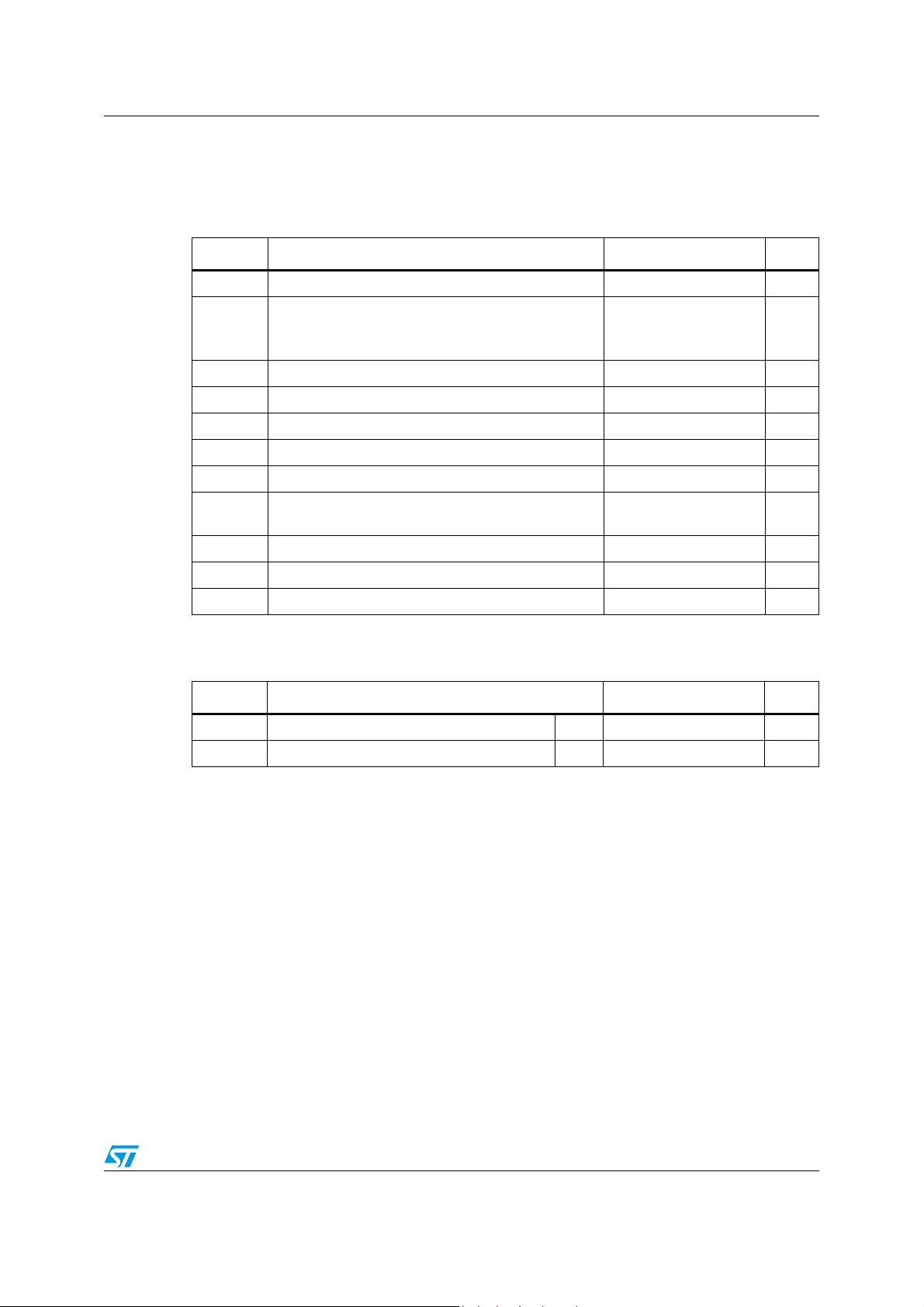
■ CMOS compatible input
■ Junction overtemperature protection
■ Case overtemperature protection for thermal
R
DS(on)
I
out
V
CC
independence of the channels
■ Current limitation
■ Shorted load protection
■ Undervoltage shutdown
■ Protection against loss of ground
■ Very low standby current
■ Compliance to 61000-4-4 IEC test up to 4 kV
Description
The VN808CM-32-E is a monolithic device
designed in STMicroelectronics VIPower M0-3
technology, intended for driving any kind of load
with one side connected to ground. It can be
driven by using a 3.3 V logic supply.
VN808CM-32-E
Octal channel high side driver
PowerSO-36
Active current limitation combined with thermal
shutdown and automatic restart, protect the
device against overload. In overload condition,
channel turns OFF and back ON automatically so
as to maintain junction temperature between T
and TR. If this condition makes case temperature
reach T
, overloaded channel is turned OFF
CSD
and will restart only when case temperature has
decreased down to T
(see waveform 3 Figure 6
CR
on page 10). Non overloaded channels continue
to operate normally. Device automatically turns
OFF in case of ground pin disconnection. This
device is especially suitable for industrial
applications conform to IEC 61131
TSD
February 2010 Doc ID 12436 Rev 4 1/21
www.st.com
21

Contents VN808CM-32-E
Contents
1 Maximum ratings . . . . . . . . . . . . . . . . . . . . . . . . . . . . . . . . . . . . . . . . . . . . 3
2 Electrical characteristics . . . . . . . . . . . . . . . . . . . . . . . . . . . . . . . . . . . . . 4
3 Pin connections . . . . . . . . . . . . . . . . . . . . . . . . . . . . . . . . . . . . . . . . . . . . . 6
4 Current, voltage conventions and truth table . . . . . . . . . . . . . . . . . . . . . 8
5 Switching time waveforms . . . . . . . . . . . . . . . . . . . . . . . . . . . . . . . . . . . . 9
6 Reverse polarity protection . . . . . . . . . . . . . . . . . . . . . . . . . . . . . . . . . . 12
7 Package mechanical data . . . . . . . . . . . . . . . . . . . . . . . . . . . . . . . . . . . . 13
7.1 Footprint recommended data . . . . . . . . . . . . . . . . . . . . . . . . . . . . . . . . . . 15
7.2 Tube shipment information . . . . . . . . . . . . . . . . . . . . . . . . . . . . . . . . . . . . 16
7.3 Tape and reel shipment information . . . . . . . . . . . . . . . . . . . . . . . . . . . . . 17
8 Order codes . . . . . . . . . . . . . . . . . . . . . . . . . . . . . . . . . . . . . . . . . . . . . . . 19
9 Revision history . . . . . . . . . . . . . . . . . . . . . . . . . . . . . . . . . . . . . . . . . . . 20
2/21 Doc ID 12436 Rev 4
VN808CM-32-E Maximum ratings
1 Maximum ratings
Table 1. Absolute maximum rating
Symbol Parameter Value Unit
V
-I
I
-I
V
P
L
T
GND
OUT
OUT
I
ESD
TOT
MAX
T
T
STG
DC supply voltage 45 V
CC
DC ground pin reverse current
TRAN ground pin reverse current
(pulse duration < 1ms)
-250
-6
DC output current Internally limited A
Reverse DC output current -2 A
DC Input current ± 10 mA
IN
Electrostatic discharge (R = 1.5 kΩ; C = 100 pF) 2000 V
Power dissipation at Tc = 25 °C 96 W
Max inductive load (VCC = 24 V, R
= 100 °C)
T
A
Junction operating temperature Internally limited °C
J
Case operating temperature Internally limited °C
C
LOAD
= 48 Ω,
2H
Storage temperature -40 to 150 °C
mA
Table 2. Thermal data
Symbol Parameter Value Unit
R
thJC
R
thJA
1. When mounted on FR4 printed circuit board with 0.5 cm2 of copper area (at least 35 μm think) connected to
all TAB pins.
Thermal resistance junction-case Max 1.3 °C/W
Thermal resistance junction-ambient
(1)
Max 50 °C/W
A
Doc ID 12436 Rev 4 3/21
Electrical characteristics VN808CM-32-E
2 Electrical characteristics
(10.5 V < VCC < 32 V; -40 °C < TJ < 125 °C; unless otherwise specified)
Table 3. Power section
Symbol Parameter Test conditions Min Typ Max Unit
Operating supply
CC
voltage
Undervoltage
shutdown
On state resistance
ON
I
OUT
I
OUT
V
V
USD
R
OFF state; V
T
I
S
I
LGND
I
L(off)
V
OUT(off)
t
d(Vccon)
Supply current
Output current at
turn-off
OFF state output
current
OFF state output
voltage
Power-on delay time
from V
rising edge
CC
CASE
ON state (all channels ON);
V
CC
V
CC
V
OUT
V
IN
V
IN
Figure 7 on page 12 1ms
Table 4. Switching (VCC = 24 V)
= 0.5 A; TJ = 25 °C
= 0.5 A;
= 24 V;
CC
= 25 °C
= 24 V, T
= V
STAT
= 100 °C
CASE
= VIN = V
= 0 V
= V
= 0 V, I
OUT
= 0 V
;
= 0 A 3 V
OUT
GND
= 24 V
10.5 45 V
710.5V
160
280mΩmΩ
15012μA
mA
1mA
05μA
Symbol Parameter Test conditions Min Typ Max Unit
= 48 Ω from 80%
R
t
t
OFF
dV
OUT/dt(on)
dV
OUT/dt(off)
ON
Turn-on time
Turn-off time RL = 48 Ω to 10% V
Turn-on voltage slope
Turn-off voltage slope
L
Figure 4.
V
OUT
R
= 48 Ω from V
L
= 19.2 V Figure 4.
V
OUT
R
= 48 Ω from V
L
= 2.4 V Figure 4.
V
OUT
4/21 Doc ID 12436 Rev 4
-50100μs
Figure 4. -75150μs
OUT
= 2.4 V to
OUT
= 21.6 V to
OUT
-0.7 V/μs
-1.5 V/μs
VN808CM-32-E Electrical characteristics
Table 5. Input pin
Symbol Parameter Test conditions Min Typ Max Unit
V
I
V
I
INH
V
I(HYST)
V
INL
INH
Input low-level 1.25 V
INL
Low-level input
current
= 1.25 V 1 μΑ
V
IN
Input high-level 2.25 V
High-level input
current
Input hysteresis
voltage
Input clamp voltage
ICL
= 2.25 V 10 μΑ
V
IN
0.25 V
I
IN
I
IN
= 1 mA
= -1 mA
6.0
6.8
-0.7
8.0
Table 6. Protections
Symbol Parameter Test conditions Min Typ Max Unit
CR
Case shutdown
temperature
Case reset
temperature
Case thermal
hysteresis
125 130 135 °C
110 °C
715 °C
T
CSD
T
T
CHYST
V
V
T
T
HYST
I
V
demag
TSD
T
lim
Junction shutdown
temperature
Junction reset
R
temperature
Junction thermal
hysteresis
DC short-circuit
current
Turn-off output clamp
voltage
150 175 200 °C
135 °C
715 °C
= 24 V; R
V
CC
= 0.5 A; L = 6 mH VCC-57 VCC-52 VCC-47 V
I
OUT
= 10 mΩ 11.7A
LOAD
Table 7. Status pin
Symbol Parameter Test conditions Min Typ Max Unit
I
HSTAT
I
LSTAT
V
CLSTAT
= 18...32 V; R
High-level output
current
V
CC
(Fault condition)
Leakage current Normal operation; V
I
= 1 mA
Clamp voltage
STAT
I
STAT
= -1 mA
= 1 kΩ
STAT
= 32 V 0.1 μA
CC
234mA
6.0 6.8
-0.7
8.0 V
V
Doc ID 12436 Rev 4 5/21
Pin connections VN808CM-32-E
3 Pin connections
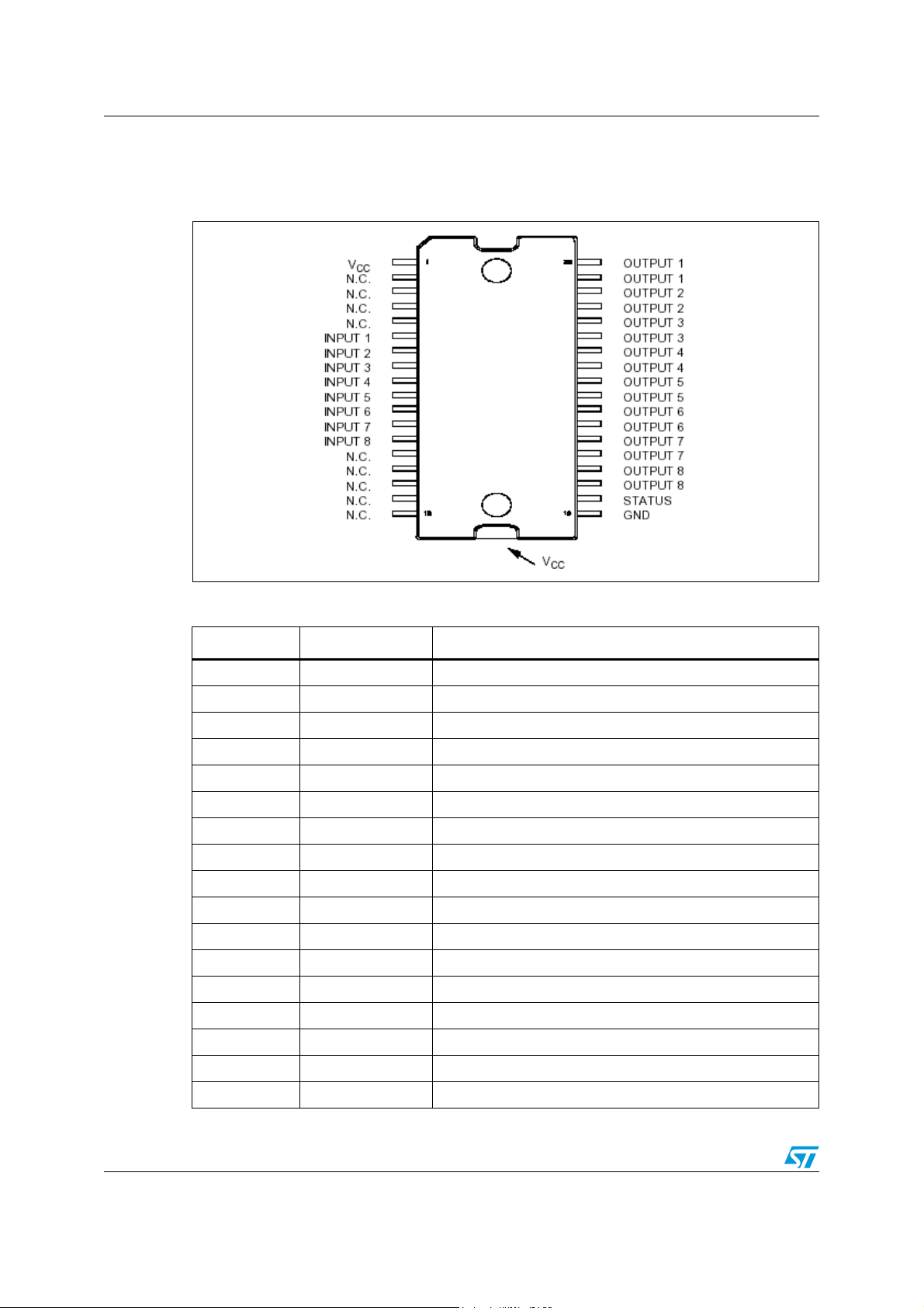
Figure 2. Connection diagram (top view)
Table 8. Pin functions
Pin N° Symbol Function
TA B V
1V
2,3,4,5 NC Not connected
6 Input 1 Input of channel 1
7 Input 2 Input of channel 2
8 Input 3 Input of channel 3
9 Input 4 Input of channel 4
10 Input 5 Input of channel 5
11 Input 6 Input of channel 6
12 Input 7 Input of channel 7
13 Input 8 Input of channel 8
14,15,16,17,18 NC Not connected
19 GND Logic ground
20 STATUS Common open source diagnostic for over-temperature
21,22 Output 8 High-side output of channel 8
23,24 Output 7 High-side output of channel 7
CC
CC
Positive power supply voltage
Positive power supply voltage
25,26 Output 6 High-side output of channel 6
6/21 Doc ID 12436 Rev 4

VN808CM-32-E Pin connections
Table 8. Pin functions (continued)
Pin N° Symbol Function
27.28 Output 5 High-side output of channel 5
29,30 Output 4 High-side output of channel 4
31,32 Output 3 High-side output of channel 3
33,34 Output 2 High-side output of channel 2
35,36 Output 1 High-side output of channel 1
Doc ID 12436 Rev 4 7/21
 Loading...