

Features
VN751S
High side driver
Typ e R
DS(on)
I
out
V
CC
VN751S 60 mΩ 2.5 A 36 V
■ CMOS compatible input
■ Thermal shutdown
■ Shorted load protection
■ Undervoltage and overvoltage shutdown
■ Protection against loss of ground
■ Very low standby current
■ Compliance to 61000-4-4 IEC test up to 4 kV
■ Open drain status output
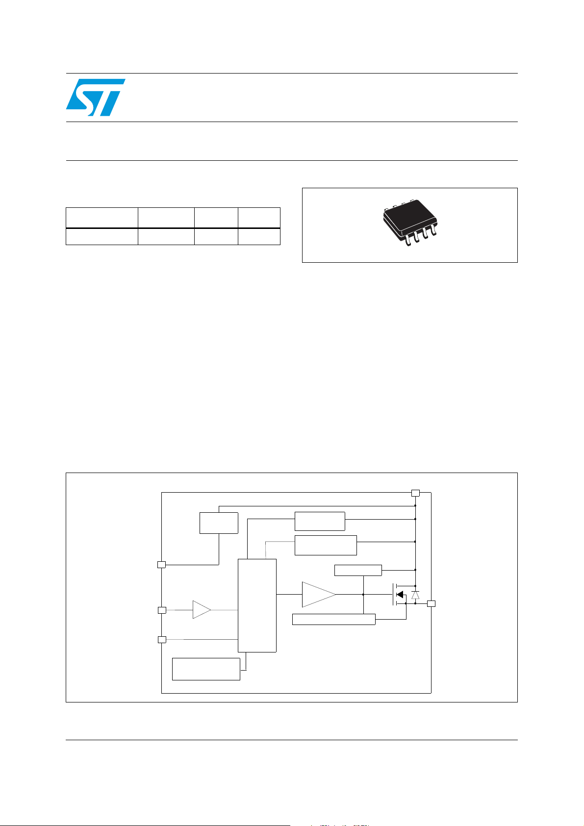
Figure 1. Block diagram
SO-8
Description
The VN751S is a monolithic device designed in
STMicroelectronics VIPower M0-3 technology,
intended for driving any kind of load with one side
connected to ground. Active V
clamp protects the device against low energy
spikes. Active current limitation combined with
thermal shutdown and automatic restart protect
the device against overload. Device automatically
turns off in case of ground pin disconnection. This
device is especially suitable for industrial
applications in conformity with IEC 61131-2
programmable controllers international standard.
V
CC
pin voltage
CC
OVERVOLTAGE
DETECTION
UNDERVOLTAGE
DETECTION
Power CLAMP
DRIVER
CURRENT LIMITER
OUTPUT
GND
INPUT
STATUS
V
CC
CLAMP
OVERTEMPERATURE
DETECTION
LOGIC
November 2009 Doc ID 12320 Rev 7 1/17
www.st.com
17

Contents VN751S
Contents
1 Maximum ratings . . . . . . . . . . . . . . . . . . . . . . . . . . . . . . . . . . . . . . . . . . . . 3
2 Pin connections . . . . . . . . . . . . . . . . . . . . . . . . . . . . . . . . . . . . . . . . . . . . . 4
3 Electrical characteristics . . . . . . . . . . . . . . . . . . . . . . . . . . . . . . . . . . . . . 5
4 Waveforms and truth table . . . . . . . . . . . . . . . . . . . . . . . . . . . . . . . . . . . . 7
5 Test circuit . . . . . . . . . . . . . . . . . . . . . . . . . . . . . . . . . . . . . . . . . . . . . . . . . 9
6 Application schematic . . . . . . . . . . . . . . . . . . . . . . . . . . . . . . . . . . . . . . 10
7 Reverse polarity protection . . . . . . . . . . . . . . . . . . . . . . . . . . . . . . . . . . 11
8 Package mechanical data . . . . . . . . . . . . . . . . . . . . . . . . . . . . . . . . . . . . 12
9 Order code . . . . . . . . . . . . . . . . . . . . . . . . . . . . . . . . . . . . . . . . . . . . . . . . 15
10 Revision history . . . . . . . . . . . . . . . . . . . . . . . . . . . . . . . . . . . . . . . . . . . 16
2/17 Doc ID 12320 Rev 7

VN751S Maximum ratings
1 Maximum ratings
Table 1. Absolute maximum rating
Symbol Parameter Value Unit
V
- V
- I
I
- I
I
V
T
E
OUT
I
STAT
ESD
P
T
T
DC supply voltage (overvoltage protected) 45 V
CC
Reverse DC supply voltage -0.3 V
CC
DC reverse ground pin current -200 mA
GND
DC output current Internally limited A
Reverse DC output current -5 A
OUT
DC input current +/- 10 mA
IN
DC status current +/- 10 mA
Electrostatic discharge (R = 1.5 kΩ; C = 100 pF) 5000 V
Power dissipation TC = 25 °C
tot
Junction operating temperature Internally limited °C
J
Case operating temperature - 40 to 150 °C
c
Storage temperature - 55 to 150 °C
stg
Single-pulse avalanche energy 0.8 J
AS
Internally limited W
Table 2. Thermal data
Symbol Parameter Value Unit
(1)
R
R
1. When mounted on a standard single-sided FR-4 board with 0.5 cm2 of Cu (at least 35μm) thick connected
to all V
2. When mounted on a standard single-sided FR-4 board with 2 cm2 of Cu (at least 35μm) thick connected to
all V
Thermal resistance junction-ambient Max
thJA
Thermal resistance junction-case Max 15 °C/W
thJC
pins. Horizontal mounting and no artificial air flow.
CC
pins. Horizontal mounting and no artificial air flow.
CC
93
82
(2)
°C/W
°C/W
Doc ID 12320 Rev 7 3/17
Pin connections VN751S
2 Pin connections
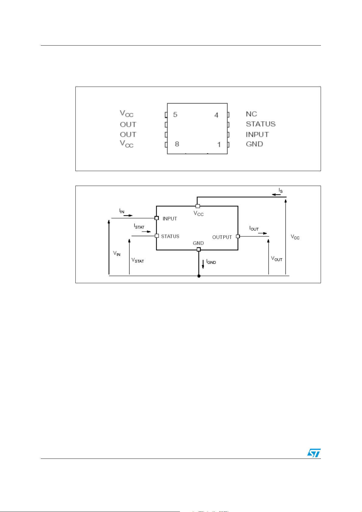
Figure 2. Connection diagram (top view)
Figure 3. Current and voltage conventions
4/17 Doc ID 12320 Rev 7
VN751S Electrical characteristics
3 Electrical characteristics
8 V < V
< 36 V; -40 °C < TJ < 125 °C, unless otherwise specified
CC
Table 3. Power
Symbol Parameter Test conditions Min Typ Max Unit
V
V
V
R
I
L(off)
CC
USD
OV
ON
I
Operating supply
voltage
Undervoltage
shut-down
Overvoltage
shut-down
On state resistance
Supply current
S
Off state output current
I
= 2 A; TJ = 25 °C
OUT
= 2 A
I
OUT
Off state; V
On state; V
On state; V
= V
V
IN
OUT
= 24 V; T
CC
= 24 V
CC
= 24 V;T
CC
= 0 V
CASE
CASE
=25 °C
=100 °C
5.5 36 V
345.5V
36 V
60
180mΩmΩ
10
20
1.5
1.8
010μA
Table 4. Switching (VCC = 24 V)
Symbol Parameter Test conditions Min Typ Max Unit
μA
mA
mA
dV
dV
t
d(on)
t
d(off)
OUT
OUT
/dt
/dt
Turn-on delay time
Turn-off delay time
Turn -on voltage slope
(on)
Turn -off voltage slope
(off)
= 12 Ω from VIN rising edge to
R
L
V
= 2.4 V
OUT
= 12 Ω from VIN falling edge to
R
L
= 21.6 V
V
OUT
= 12Ω from V
R
L
= 19.2 V
V
OUT
= 12 Ω from V
R
L
= 2.4 V
V
OUT
= 2.4 V to
OUT
= 21.6 V to
OUT
12 μs
35 μs
0.80 V/μs
0.30 V/μs
Doc ID 12320 Rev 7 5/17
Electrical characteristics VN751S
Table 5. Input pin
Symbol Parameter Test conditions Min Typ Max Unit
V
IL
I
IL
V
IH
I
IH
V
hyst
I
IN
V
ICL
Input low level 1.25 V
Low level input
current
V
= 1.25 V
IN
1 μA
Input high level 3.25 V
High level input
current
Input hysteresis
voltage
Input current
Input clamp voltage
V
= 3.25 V
IN
V
IN = VCC
I
= 1 mA
IN
= -1 mA
I
IN
= 5 V
0.5 V
6
6.8
-0.7
10 μA
10 μA
8 V
Table 6. Status pin
Symbol Parameter Test conditions Min Typ Max Unit
V
STAT
I
LSTAT
C
STAT
V
SCL
Status low output
voltage
Status leakage
current
Status pin input
capacitance
Status clamp voltage
I
= 1.6 mA
STAT
Normal operation; V
Normal operation; V
= 1 mA;
I
STAT
=-1 mA
I
STAT
STAT
STAT
= 5 V
= 5 V
6 6.8
-0.7
0.5 V
10 µA
100 pF
8 V
V
V
Table 7. Protections
Symbol Parameter Test conditions Min Typ Max Unit
T
TSD
T
R
T
hyst
I
lim
V
demag
6/17 Doc ID 12320 Rev 7
Shut-down
temperature
Reset temperature 135 °C
Thermal hysteresis 7 20 °C
Current limitation
CC
t = 0.4 ms
LOAD
V
= 24 V, R
Turn-off output
clamp
RL =12 Ω; L = 6 mH
voltage
= 10 mΩ,
150 175 200 °C
2.7 6.0 A
V
-47VCC-52VCC-
CC
57
V
 Loading...