

Features
Type R
VN750SM 55 mΩ 6 A 36 V
DS(on)
I
OUT
VN750SM
High-side driver
V
CC
■ CMOS compatible input
■ On-state open load detection
■ Off-state open load detection
■ Shorted load protection
■ Under-voltage and over-voltage shutdown
■ Protection against loss of ground
■ Very low stand-by current
■ Reverse battery protected (see Application
schematic
)
SO-8
Description
The VN750SM is a monolithic device designed in
STMicroelectronics VIPower M0-3 technology.
The VN750SM is intended for driving any type of
load with one side connected to ground. The
active V
against low energy spikes (see ISO7637 transient
compatibility table).
Active current limitation combined with thermal
shutdown and automatic restart protects the
device against over-load. The device detects the
open load condition in both the on and off-state.
The open load threshold is aimed at detecting the
5 W / 12 V standard bulb as an open load fault in
the on-state.
In the off-state the device detects if the output is
shorted to V
in the case where the ground pin becomes
disconnected.
pin voltage clamp protects the device
CC
. The device automatically turns off
CC
Table 1. Device summary
Order codes
Package
Tube Tape and reel
SO-8 VN750SM VN750SM13TR
December 2008 Rev 3 1/27
www.st.com
27

Contents VN750SM
Contents
1 Block diagram and pin description . . . . . . . . . . . . . . . . . . . . . . . . . . . . . 5
2 Electrical specifications . . . . . . . . . . . . . . . . . . . . . . . . . . . . . . . . . . . . . . 6
2.1 Absolute maximum ratings . . . . . . . . . . . . . . . . . . . . . . . . . . . . . . . . . . . . . 6
2.2 Thermal data . . . . . . . . . . . . . . . . . . . . . . . . . . . . . . . . . . . . . . . . . . . . . . . 7
2.3 Electrical characteristics . . . . . . . . . . . . . . . . . . . . . . . . . . . . . . . . . . . . . . . 7
2.4 Electrical characteristics curves . . . . . . . . . . . . . . . . . . . . . . . . . . . . . . . . 13
3 Application information . . . . . . . . . . . . . . . . . . . . . . . . . . . . . . . . . . . . . 16
3.1 GND protection network against reverse battery . . . . . . . . . . . . . . . . . . . 16
3.1.1 Solution 1: resistor in the ground line (RGND only) . . . . . . . . . . . . . . . . 16
3.1.2 Solution 2: diode (DGND) in the ground line . . . . . . . . . . . . . . . . . . . . . 17
3.2 Load dump protection . . . . . . . . . . . . . . . . . . . . . . . . . . . . . . . . . . . . . . . . 17
3.3 MCU I/Os protection . . . . . . . . . . . . . . . . . . . . . . . . . . . . . . . . . . . . . . . . . 17
3.4 Open load detection in off-state . . . . . . . . . . . . . . . . . . . . . . . . . . . . . . . . 18
3.5 Maximum demagnetization energy (VCC = 13.5V) . . . . . . . . . . . . . . . . . 19
4 Package and PCB thermal data . . . . . . . . . . . . . . . . . . . . . . . . . . . . . . . 20
4.1 SO-8 thermal data . . . . . . . . . . . . . . . . . . . . . . . . . . . . . . . . . . . . . . . . . . 20
5 Package and packing information . . . . . . . . . . . . . . . . . . . . . . . . . . . . . 23
5.1 ECOPACK® packages . . . . . . . . . . . . . . . . . . . . . . . . . . . . . . . . . . . . . . . 23
5.2 SO-8 package information . . . . . . . . . . . . . . . . . . . . . . . . . . . . . . . . . . . . 23
5.3 SO-8 packing information . . . . . . . . . . . . . . . . . . . . . . . . . . . . . . . . . . . . . 25
6 Revision history . . . . . . . . . . . . . . . . . . . . . . . . . . . . . . . . . . . . . . . . . . . 26
2/27

VN750SM List of tables
List of tables
Table 1. Device summary . . . . . . . . . . . . . . . . . . . . . . . . . . . . . . . . . . . . . . . . . . . . . . . . . . . . . . . . . . 1
Table 2. Suggested connections for unused and not connected pins . . . . . . . . . . . . . . . . . . . . . . . . 5
Table 3. Absolute maximum ratings . . . . . . . . . . . . . . . . . . . . . . . . . . . . . . . . . . . . . . . . . . . . . . . . . . 6
Table 4. Thermal data. . . . . . . . . . . . . . . . . . . . . . . . . . . . . . . . . . . . . . . . . . . . . . . . . . . . . . . . . . . . . 7
Table 5. Power . . . . . . . . . . . . . . . . . . . . . . . . . . . . . . . . . . . . . . . . . . . . . . . . . . . . . . . . . . . . . . . . . . 7
Table 6. Switching (V
Table 7. Input pin . . . . . . . . . . . . . . . . . . . . . . . . . . . . . . . . . . . . . . . . . . . . . . . . . . . . . . . . . . . . . . . . 8
Table 8. V
Table 9. Status pin . . . . . . . . . . . . . . . . . . . . . . . . . . . . . . . . . . . . . . . . . . . . . . . . . . . . . . . . . . . . . . . 8
Table 10. Protections . . . . . . . . . . . . . . . . . . . . . . . . . . . . . . . . . . . . . . . . . . . . . . . . . . . . . . . . . . . . . . 9
Table 11. Open load detection . . . . . . . . . . . . . . . . . . . . . . . . . . . . . . . . . . . . . . . . . . . . . . . . . . . . . . . 9
Table 12. Truth table. . . . . . . . . . . . . . . . . . . . . . . . . . . . . . . . . . . . . . . . . . . . . . . . . . . . . . . . . . . . . . 10
Table 13. Electrical transient requirements . . . . . . . . . . . . . . . . . . . . . . . . . . . . . . . . . . . . . . . . . . . . 11
Table 14. Thermal parameter . . . . . . . . . . . . . . . . . . . . . . . . . . . . . . . . . . . . . . . . . . . . . . . . . . . . . . . 22
Table 15. SO-8 mechanical data . . . . . . . . . . . . . . . . . . . . . . . . . . . . . . . . . . . . . . . . . . . . . . . . . . . . 24
Table 16. Document revision history . . . . . . . . . . . . . . . . . . . . . . . . . . . . . . . . . . . . . . . . . . . . . . . . . 26
output diode. . . . . . . . . . . . . . . . . . . . . . . . . . . . . . . . . . . . . . . . . . . . . . . . . . . . . . . . . . 8
CC
=13V) . . . . . . . . . . . . . . . . . . . . . . . . . . . . . . . . . . . . . . . . . . . . . . . . . . . . . . 8
CC
3/27

List of figures VN750SM
List of figures
Figure 1. Block diagram . . . . . . . . . . . . . . . . . . . . . . . . . . . . . . . . . . . . . . . . . . . . . . . . . . . . . . . . . . . . 5
Figure 2. Configuration diagram (top view) . . . . . . . . . . . . . . . . . . . . . . . . . . . . . . . . . . . . . . . . . . . . . 5
Figure 3. Current and voltage conventions . . . . . . . . . . . . . . . . . . . . . . . . . . . . . . . . . . . . . . . . . . . . . 6
Figure 4. Status timings . . . . . . . . . . . . . . . . . . . . . . . . . . . . . . . . . . . . . . . . . . . . . . . . . . . . . . . . . . . . 9
Figure 5. Switching time waveforms . . . . . . . . . . . . . . . . . . . . . . . . . . . . . . . . . . . . . . . . . . . . . . . . . 10
Figure 6. Waveforms . . . . . . . . . . . . . . . . . . . . . . . . . . . . . . . . . . . . . . . . . . . . . . . . . . . . . . . . . . . . . 12
Figure 7. Off-state output current . . . . . . . . . . . . . . . . . . . . . . . . . . . . . . . . . . . . . . . . . . . . . . . . . . . . 13
Figure 8. High level input current . . . . . . . . . . . . . . . . . . . . . . . . . . . . . . . . . . . . . . . . . . . . . . . . . . . . 13
Figure 9. Input clamp voltage. . . . . . . . . . . . . . . . . . . . . . . . . . . . . . . . . . . . . . . . . . . . . . . . . . . . . . . 13
Figure 10. Status leakage current . . . . . . . . . . . . . . . . . . . . . . . . . . . . . . . . . . . . . . . . . . . . . . . . . . . . 13
Figure 11. Status low output voltage . . . . . . . . . . . . . . . . . . . . . . . . . . . . . . . . . . . . . . . . . . . . . . . . . . 13
Figure 12. Status clamp voltage . . . . . . . . . . . . . . . . . . . . . . . . . . . . . . . . . . . . . . . . . . . . . . . . . . . . . 13
Figure 13. On-state resistance Vs T
Figure 14. On-state resistance Vs V
Figure 15. Open load on-state detection threshold . . . . . . . . . . . . . . . . . . . . . . . . . . . . . . . . . . . . . . . 14
Figure 16. Input high level . . . . . . . . . . . . . . . . . . . . . . . . . . . . . . . . . . . . . . . . . . . . . . . . . . . . . . . . . . 14
Figure 17. Input low level . . . . . . . . . . . . . . . . . . . . . . . . . . . . . . . . . . . . . . . . . . . . . . . . . . . . . . . . . . . 14
Figure 18. Input hysteresis voltage . . . . . . . . . . . . . . . . . . . . . . . . . . . . . . . . . . . . . . . . . . . . . . . . . . . 14
Figure 19. Over-voltage shutdown . . . . . . . . . . . . . . . . . . . . . . . . . . . . . . . . . . . . . . . . . . . . . . . . . . . . 15
Figure 20. Open load off-state voltage detection threshold . . . . . . . . . . . . . . . . . . . . . . . . . . . . . . . . . 15
Figure 21. Turn-on voltage slope . . . . . . . . . . . . . . . . . . . . . . . . . . . . . . . . . . . . . . . . . . . . . . . . . . . . . 15
Figure 22. Turn-off voltage slope . . . . . . . . . . . . . . . . . . . . . . . . . . . . . . . . . . . . . . . . . . . . . . . . . . . . . 15
Figure 23. I
lim
Vs T
. . . . . . . . . . . . . . . . . . . . . . . . . . . . . . . . . . . . . . . . . . . . . . . . . . . . . . . . . . . . . 15
case
Figure 24. Application schematic . . . . . . . . . . . . . . . . . . . . . . . . . . . . . . . . . . . . . . . . . . . . . . . . . . . . . 16
Figure 25. Open load detection in off-state . . . . . . . . . . . . . . . . . . . . . . . . . . . . . . . . . . . . . . . . . . . . . 18
Figure 26. Maximum turn-off current versus inductance . . . . . . . . . . . . . . . . . . . . . . . . . . . . . . . . . . . 19
Figure 27. PC board. . . . . . . . . . . . . . . . . . . . . . . . . . . . . . . . . . . . . . . . . . . . . . . . . . . . . . . . . . . . . . . 20
Figure 28. Rthj-amb Vs. PCB copper area in open box free air condition . . . . . . . . . . . . . . . . . . . . . . 20
Figure 29. SO-8 thermal impedance junction ambient single pulse . . . . . . . . . . . . . . . . . . . . . . . . . . 21
Figure 30. Thermal fitting model of a single channel . . . . . . . . . . . . . . . . . . . . . . . . . . . . . . . . . . . . . 21
Figure 31. SO-8 package dimensions . . . . . . . . . . . . . . . . . . . . . . . . . . . . . . . . . . . . . . . . . . . . . . . . . 23
Figure 32. SO-8 tube shipment (no suffix) . . . . . . . . . . . . . . . . . . . . . . . . . . . . . . . . . . . . . . . . . . . . . . 25
Figure 33. SO-8 tape and reel shipment (suffix “TR”) . . . . . . . . . . . . . . . . . . . . . . . . . . . . . . . . . . . . . 25
. . . . . . . . . . . . . . . . . . . . . . . . . . . . . . . . . . . . . . . . . . . . . . . 14
case
. . . . . . . . . . . . . . . . . . . . . . . . . . . . . . . . . . . . . . . . . . . . . . . . 14
CC
4/27
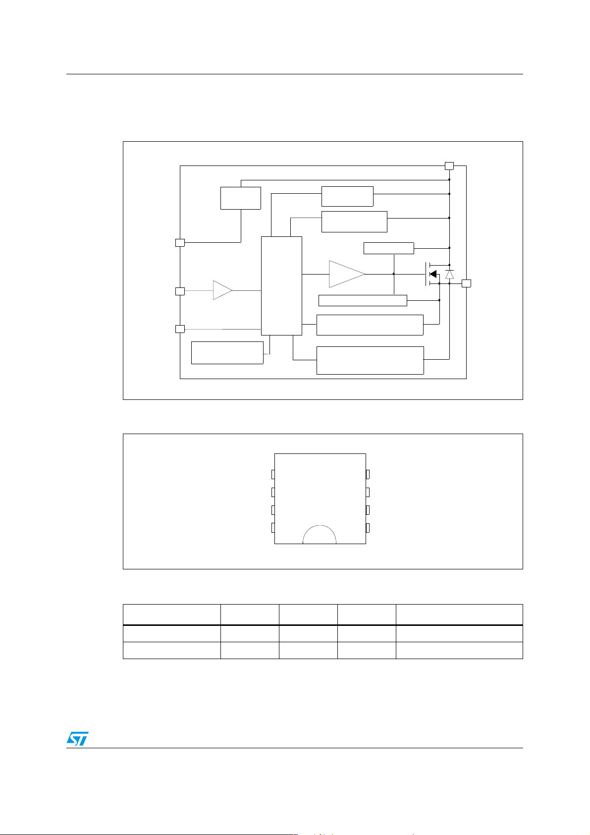
VN750SM Block diagram and pin description
1 Block diagram and pin description
Figure 1. Block diagram
V
CC
V
CC
CLAMP
GND
INPUT
LOGIC
STATUS
OVER-TEMPERATURE
DETECTION
OVER-VOLTAGE
AND OUTPUT SHORTED TO V
Figure 2. Configuration diagram (top view)
V
CC
5
OUTPUT
DETECTION
UNDER-VOLTAGE
DETECTION
Powe r CLAMP
DRIVER
CURRENT LIMITER
ON-STATE OPEN LOAD
DETECTION
OFF-STATE OPEN LOAD
DETECTION
4
N.C.
STATUS
OUTPUT
CC
OUTPUT
V
CC
Table 2. Suggested connections for unused and not connected pins
8
INPUT
1
GND
Connection / pin Status N.C. Output Input
Floating X X X X
To ground X Through 10KΩ resistor
5/27
Electrical specifications VN750SM
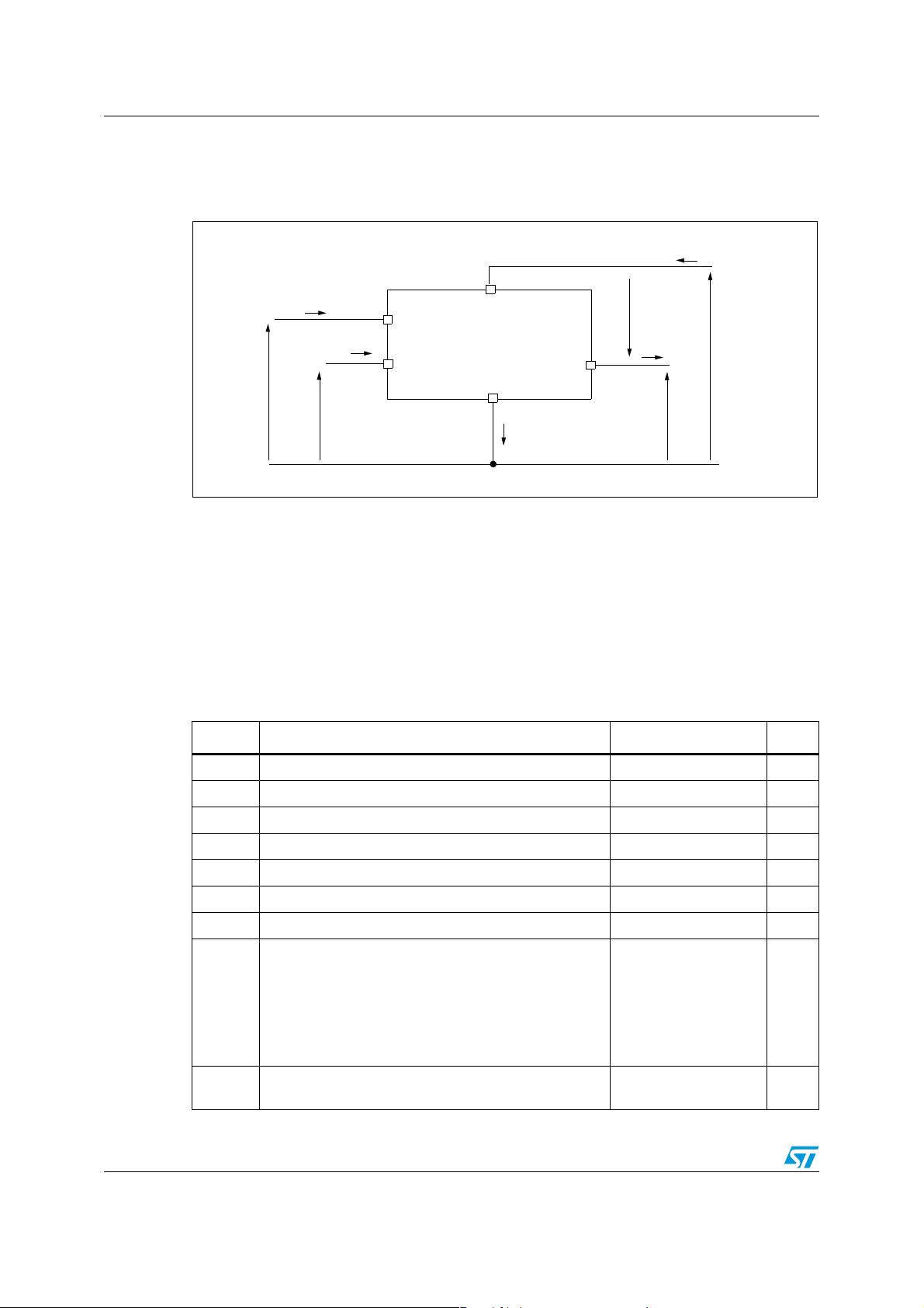
2 Electrical specifications
Figure 3. Current and voltage conventions
I
S
V
I
IN
INPUT
I
STAT
STATUS
V
IN
V
STAT
2.1 Absolute maximum ratings
V
CC
GND
OUTPUT
I
GND
F
I
OUT
V
OUT
V
CC
Stressing the device above the rating listed in the “Absolute maximum ratings” table may
cause permanent damage to the device. These are stress ratings only and operation of the
device at these or any other conditions above those indicated in the operating sections of
this specification is not implied. Exposure to Absolute maximum rating conditions for
extended periods may affect device reliability. Refer also to the STMicroelectronics sure
program and other relevant quality document.
Table 3. Absolute maximum ratings
Symbol Parameter Value Unit
V
- V
- I
I
OUT
- I
I
STAT
V
E
DC supply voltage 41 V
CC
Reverse DC supply voltage - 0.3 V
CC
DC reverse ground pin current - 200 mA
gnd
DC output current Internally limited A
Reverse DC output current - 6 A
OUT
I
DC input current +/- 10 mA
IN
DC status current +/- 10 mA
Electrostatic discharge
(human body model: R =1.5KΩ; C =100pF)
INPUT
ESD
STATUS
OUTPUT
V
CC
Maximum switching energy (L = 1.3mH; RL= 0Ω;
MAX
V
bat
= 13.5V; T
= 150ºC; IL = 10A)
jstart
4000
4000
5000
5000
90 mJ
V
V
V
V
6/27
VN750SM Electrical specifications
Table 3. Absolute maximum ratings (continued)
Symbol Parameter Value Unit
P
T
Power dissipation TC=25°C 4.2 W
tot
T
Junction operating temperature Internally limited °C
j
Storage temperature - 55 to 150 °C
stg
2.2 Thermal data
Table 4. Thermal data
Symbol Parameter Max. value Unit
R
thj-lead
R
thj-amb
1. When mounted on a standard single-sided FR-4 board with 0.5 cm2 of Cu (at least 35µm thick) connected
to all VCC pins. Horizontal mounting and no artificial air flow.
2. When mounted on a standard single-sided FR-4 board with 2 cm2 of Cu (at least 35µm thick). Horizontal
mounting and no artificial air flow.
Thermal resistance junction-lead 30 °C/W
Thermal resistance junction-ambient 93
2.3 Electrical characteristics
Values specified in this section are for 8V < V
stated.
Table 5. Power
(1)
< 36V; -40°C < Tj < 150°C, unless otherwise
CC
82
(2)
°C/W
Symbol Parameter Test conditions Min. Typ. Max. Unit
V
V
V
USDhyst
V
R
I
L(off1)
I
L(off2)
Operating supply voltage 5.5 13 36 V
CC
Under-voltage shutdown 3 4 5.5 V
USD
Under-voltage shutdown
hysteresis
Over-voltage shutdown 36 V
OV
On-state resistance
ON
Supply current
I
S
Off-state output current V
Off-state output current V
= 2A; Tj = 25°C; V
I
OUT
I
= 2A; V
OUT
Off-state; V
V
= V
IN
OUT
Off-state; V
V
= V
IN
OUT
On-state; V
I
= 0A
OUT
= V
IN
OUT
= 0V; V
IN
> 8V
CC
= 13V;
CC
= 0V
= 13V;
CC
= 0V; Tj = 25°C
= 13V; V
CC
= 0V 0 50 µA
= 3.5V -75 0 µA
OUT
CC
IN
> 8V
= 5V;
0.5 V
55
110mΩmΩ
µA
25
10
µA
20
10
mA
3.5
2
7/27
Electrical specifications VN750SM
Table 5. Power (continued)
Symbol Parameter Test conditions Min. Typ. Max. Unit
V
= V
I
L(off3)
I
L(off4)
Table 6. Switching (VCC=13V)
Off-state output current
Off-state output current
IN
= 125°C
T
j
V
= V
IN
= 25°C
T
j
Symbol Parameter Test conditions Min. Typ. Max. Unit
= 6.5Ω from VIN rising edge to
R
t
d(on)
t
d(off)
dV
OUT
dV
OUT
Table 7. Input pin
Turn-on delay time
Turn-off delay time
/dt
Turn-on voltage slope
(on)
/dt
Turn-off voltage slope
(off)
L
V
OUT
= 6.5Ω from VIN falling edge to
R
L
V
OUT
= 6.5Ω from V
R
L
V
OUT
R
= 6.5Ω from V
L
V
OUT
OUT
OUT
= 1.3V
= 11.7V
=10.4V
=1.3V
= 0V; V
= 0V; V
= 13V;
CC
= 13V;
CC
= 1.3V to
OUT
= 11.7V to
OUT
5µA
3µA
40 µs
30 µs
See Figure 21. V/µs
See Figure 22. V/µs
Symbol Parameter Test conditions Min. Typ. Max. Unit
V
V
V
V
Table 8. VCC output diode
Input low level 1.25 V
IL
Low level input current V
I
IL
Input high level 3.25 V
IH
High level input current V
I
IH
Input hysteresis voltage 0.5 V
hyst
Input clamp voltage
ICL
= 1.25V 1 µA
IN
= 3.25V 10 µA
IN
I
IN
I
IN
= 1mA
= -1mA
66.8
- 0.7
8V
Symbol Parameter Test conditions Min. Typ. Max. Unit
V
F
Table 9. Status pin
Forward on voltage - I
= 1.4A; Tj = 150°C 0.6 V
OUT
Symbol Parameter Test conditions Min. Typ. Max. Unit
V
STAT
I
LSTAT
C
STAT
V
SCL
Status low output voltage I
Status leakage current Normal operation; V
Status pin input capacitance Normal operation; V
Status clamp voltage
= 1.6mA 0.5 V
STAT
= 5V 10 µA
STAT
= 5V 100 pF
STAT
I
STAT
I
STAT
= 1mA
= - 1mA
66.8
- 0.7
8V
V
V
8/27
VN750SM Electrical specifications
Table 10. Protections
(1)
Symbol Parameter Test conditions Min. Typ. Max. Unit
T
TSD
T
T
hyst
t
SDL
I
V
demag
1. To ensure long term reliability under heavy over-load or short circuit conditions, protection and related
diagnostic signals must be used together with a proper software strategy. If the device operates under
abnormal conditions this software must limit the duration and number of activation cycles.
Table 11. Open load detection
Shutdown temperature 150 175 200 °C
Reset temperature 135 °C
R
Thermal hysteresis 7 15 °C
Status delay in over-load
condition
Current limitation
lim
Turn-off output clamp
voltage
I
OUT
T
9V < V
5V < V
= 2 A; V
L = 6mH
j
> T
CC
CC
jsh
< 36V
< 36V
= 0V;
IN
6101212A
V
CC
- 41 V
CC
- 48 V
20 µs
- 55 V
CC
Symbol Parameter Test conditions Min. Typ. Max. Unit
I
OL
Open load on-state
detection threshold
V
= 5V 0.6 0.9 1.2 A
IN
A
t
DOL(on)
Open load on-state
detection delay
Open load off-state
V
voltage detection
OL
threshold
Open load detection
delay at turn-off
t
DOL(off)
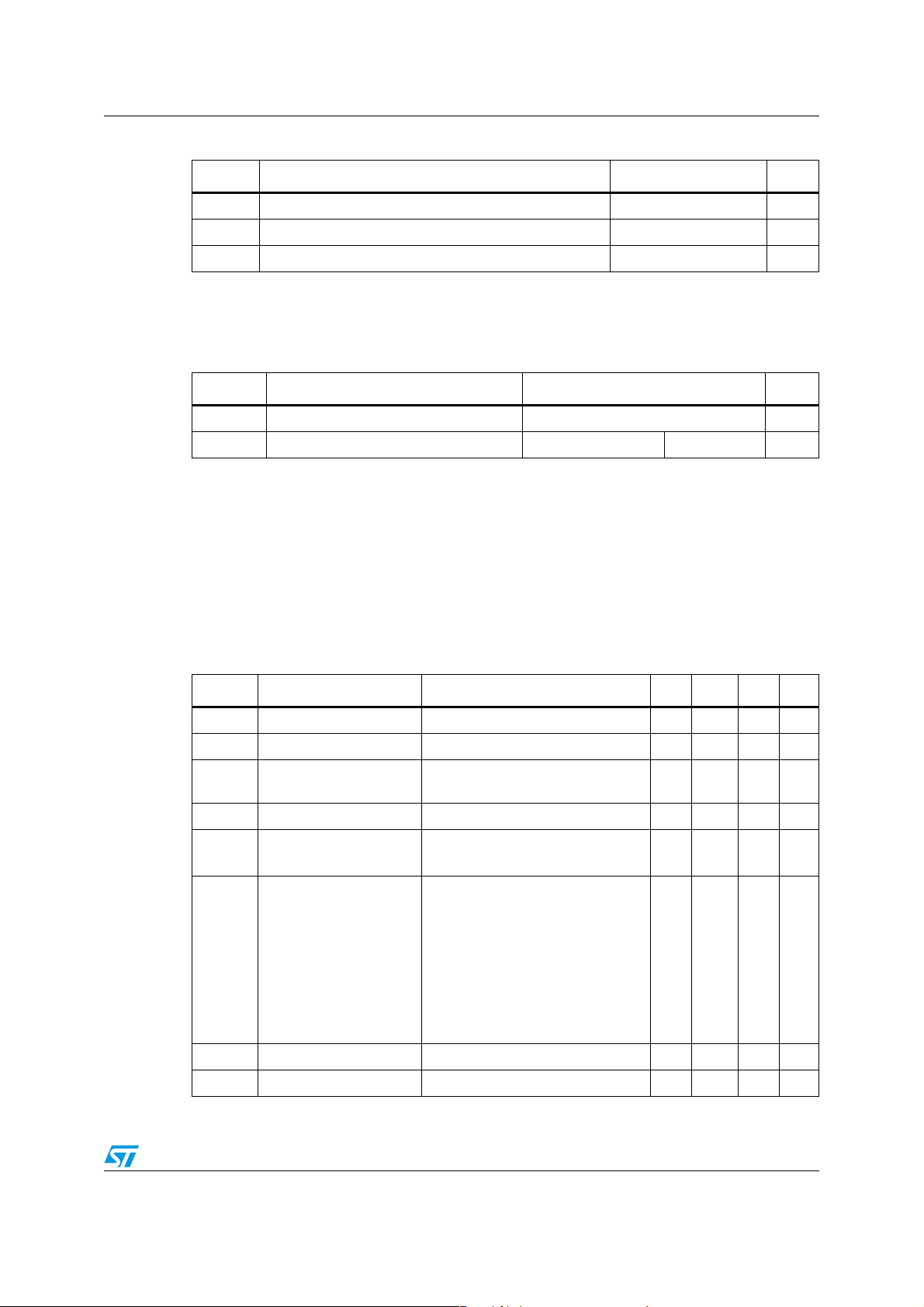
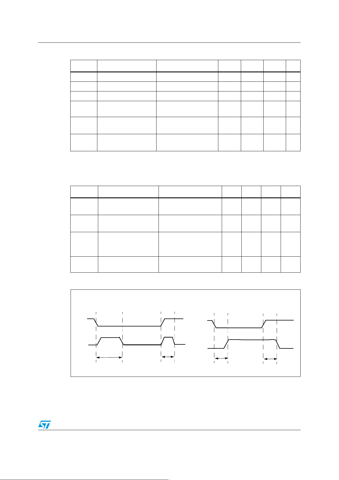
Figure 4. Status timings
OPEN LOAD STATUS TIMING (with external pull-up)
V
> V
OUT
OL
V
IN
V
STAT
t
DOL(off)
t
I
OUT
DOL(on)
< I
I
= 0A 200 µs
OUT
V
= 0V 1.5 2.5 3.5 V
IN
OVER-TEMP STATUS TIMING
OL
Tj > T
jsh
V
V
IN
STAT
t
SDL
1000 µs
t
SDL
9/27
 Loading...