


Features
VN5772AK-E
Quad smart power solid-state relay
for complete H-bridge configurations
Typ e R
VN5772AK-E 100 mΩ
1. Total resistance of one side in bridge configuration.
2. Typical current limitation value.
■ General features
DS(on)
(1)
I
OUT
18 A
(2)
– Inrush current management by active
power limitation on the high-side switches
– Very low standby current
– Very low electromagnetic susceptibility
– Compliant with European directive
2002/95/EC
■ Protections
– High-side drivers under voltage shutdown
– Overvoltage clamp
– Output current limitation
– High and low-side overtemperature
shutdown
– Short-circuit protection
– ESD protection
■ Diagnostic functions
– Proportional load current sense
– Thermal shutdown indication on both the
high and low-side switches
Applications
■ DC motor driving in full or half-bridge
configuration
■ All types of resistive, inductive and capacitive
loads
Table 1. Device summary
Package
V
CC
36 V
SO-28
Description
The VN5772AK-E is a device formed by three
monolithic chips housed in a standard SO-28
package: a double high-side and two low-side
switches. The double high-side is made using
STMicroelectronics
while the low-side switches are fully protected
VIPower M0-5 OMNIFET III. This device is
suitable to drive a DC motor in a bridge
configuration as well as to be used as a quad
switch for any low-voltage application. The dual
high-side switches integrate built-in non latching
thermal shutdown with thermal hysteresis. An
output current limiter protects the device in
overload conditions. In the case of long overload
duration, the device limits the dissipated power to
a safe level-up to thermal shutdown intervention.
An analog current sense pin delivers a current
proportional to the load current (according to a
known ratio) and indicates overtemperature
shutdown of the relevant high-side switch through
a voltage flag.The low-side switches have built-in
non latching thermal shutdown with thermal
hysteresis, linear current limitation and
overvoltage clamping. In case of long overload
duration, the low-side switches limit the dissipated
power to a safe level up to the thermal shutdown
intervention. Fault feedback for overtemperature
shutdown of the low-side switch is indicated by
the relevant status pin.
Order codes
Tube Tape and reel
®
VIPower® M0-5 technology,
SO-28 VN5772AK-E VN5772AKTR-E
November 2011 Doc ID 16084 Rev 5 1/34
www.st.com
1

Contents VN5772AK-E
Contents
1 Block diagram and pin description . . . . . . . . . . . . . . . . . . . . . . . . . . . . . 5
2 Electrical specification . . . . . . . . . . . . . . . . . . . . . . . . . . . . . . . . . . . . . . . 7
2.1 Absolute maximum ratings . . . . . . . . . . . . . . . . . . . . . . . . . . . . . . . . . . . . . 7
2.2 Thermal data . . . . . . . . . . . . . . . . . . . . . . . . . . . . . . . . . . . . . . . . . . . . . . . 8
2.3 Electrical characteristics . . . . . . . . . . . . . . . . . . . . . . . . . . . . . . . . . . . . . . . 9
2.3.1 Electrical characteristics for dual high-side switches . . . . . . . . . . . . . . . . 9
2.4 Electrical characteristics curves for dual high-side switches . . . . . . . . . . 15
2.5 Electrical characteristics for low-side switch . . . . . . . . . . . . . . . . . . . . . . . 17
2.6 Electrical characteristics curves for low-side switch . . . . . . . . . . . . . . . . . 19
3 Application information . . . . . . . . . . . . . . . . . . . . . . . . . . . . . . . . . . . . . 21
3.1 Maximum demagnetization energy (V
= 13.5 V) . . . . . . . . . . . . . . . . . 24
CC
4 Package and PC board thermal data . . . . . . . . . . . . . . . . . . . . . . . . . . . 25
4.1 SO-28 thermal data . . . . . . . . . . . . . . . . . . . . . . . . . . . . . . . . . . . . . . . . . 25
5 Package and packing information . . . . . . . . . . . . . . . . . . . . . . . . . . . . . 30
5.1 ECOPACK® package . . . . . . . . . . . . . . . . . . . . . . . . . . . . . . . . . . . . . . . . 30
5.2 Package mechanical data . . . . . . . . . . . . . . . . . . . . . . . . . . . . . . . . . . . . 30
5.3 Packing information . . . . . . . . . . . . . . . . . . . . . . . . . . . . . . . . . . . . . . . . . 32
6 Revision history . . . . . . . . . . . . . . . . . . . . . . . . . . . . . . . . . . . . . . . . . . . 33
2/34 Doc ID 16084 Rev 5

VN5772AK-E List of tables
List of tables
Table 1. Device summary . . . . . . . . . . . . . . . . . . . . . . . . . . . . . . . . . . . . . . . . . . . . . . . . . . . . . . . . . . 1
Table 2. Pin description . . . . . . . . . . . . . . . . . . . . . . . . . . . . . . . . . . . . . . . . . . . . . . . . . . . . . . . . . . . 6
Table 3. Dual high-side switch . . . . . . . . . . . . . . . . . . . . . . . . . . . . . . . . . . . . . . . . . . . . . . . . . . . . . . 7
Table 4. Low side switch. . . . . . . . . . . . . . . . . . . . . . . . . . . . . . . . . . . . . . . . . . . . . . . . . . . . . . . . . . . 8
Table 5. Thermal data. . . . . . . . . . . . . . . . . . . . . . . . . . . . . . . . . . . . . . . . . . . . . . . . . . . . . . . . . . . . . 8
Table 6. Power section . . . . . . . . . . . . . . . . . . . . . . . . . . . . . . . . . . . . . . . . . . . . . . . . . . . . . . . . . . . . 9
Table 7. Switching (VCC = 13 V) . . . . . . . . . . . . . . . . . . . . . . . . . . . . . . . . . . . . . . . . . . . . . . . . . . . . 9
Table 8. Logic inputs. . . . . . . . . . . . . . . . . . . . . . . . . . . . . . . . . . . . . . . . . . . . . . . . . . . . . . . . . . . . . 10
Table 9. Protection and diagnostics . . . . . . . . . . . . . . . . . . . . . . . . . . . . . . . . . . . . . . . . . . . . . . . . . 10
Table 10. Current sense (8 V < VCC < 16 V) . . . . . . . . . . . . . . . . . . . . . . . . . . . . . . . . . . . . . . . . . . . 11
Table 11. Truth table high-side driver . . . . . . . . . . . . . . . . . . . . . . . . . . . . . . . . . . . . . . . . . . . . . . . . . 13
Table 12. Electrical transient requirements (part 1/3) . . . . . . . . . . . . . . . . . . . . . . . . . . . . . . . . . . . . . 14
Table 13. Electrical transient requirements (part 2/3) . . . . . . . . . . . . . . . . . . . . . . . . . . . . . . . . . . . . . 14
Table 14. Electrical transient requirements (part 3/3) . . . . . . . . . . . . . . . . . . . . . . . . . . . . . . . . . . . . . 14
Table 15. PowerMOS section - off . . . . . . . . . . . . . . . . . . . . . . . . . . . . . . . . . . . . . . . . . . . . . . . . . . . 17
Table 16. PowerMOS section - on . . . . . . . . . . . . . . . . . . . . . . . . . . . . . . . . . . . . . . . . . . . . . . . . . . . 17
Table 17. Switching (T
Table 18. Source drain diode . . . . . . . . . . . . . . . . . . . . . . . . . . . . . . . . . . . . . . . . . . . . . . . . . . . . . . . 17
Table 19. Input section . . . . . . . . . . . . . . . . . . . . . . . . . . . . . . . . . . . . . . . . . . . . . . . . . . . . . . . . . . . . 17
Table 20. STATUS pin . . . . . . . . . . . . . . . . . . . . . . . . . . . . . . . . . . . . . . . . . . . . . . . . . . . . . . . . . . . . 18
Table 21. Protection and diagnostics (-40 °C < Tj < 150 °C, unless otherwise specified) . . . . . . . . . 18
Table 22. Truth table low-side driver . . . . . . . . . . . . . . . . . . . . . . . . . . . . . . . . . . . . . . . . . . . . . . . . . 18
Table 23. Thermal calculations in clockwise and anti-clockwise operation in steady-state mode . . . 26
Table 24. Thermal resistances definitions . . . . . . . . . . . . . . . . . . . . . . . . . . . . . . . . . . . . . . . . . . . . . 26
Table 25. Single pulse thermal impedance definitions . . . . . . . . . . . . . . . . . . . . . . . . . . . . . . . . . . . . 26
Table 26. Thermal calculations in transient mode . . . . . . . . . . . . . . . . . . . . . . . . . . . . . . . . . . . . . . . 27
Table 27. Thermal parameters . . . . . . . . . . . . . . . . . . . . . . . . . . . . . . . . . . . . . . . . . . . . . . . . . . . . . . 29
Table 28. SO-28 mechanical data . . . . . . . . . . . . . . . . . . . . . . . . . . . . . . . . . . . . . . . . . . . . . . . . . . . 31
Table 29. Document revision history . . . . . . . . . . . . . . . . . . . . . . . . . . . . . . . . . . . . . . . . . . . . . . . . . 33
= 25° C, unless otherwise specified) . . . . . . . . . . . . . . . . . . . . . . . . . . . . . . . 17
j
Doc ID 16084 Rev 5 3/34

List of figures VN5772AK-E
List of figures
Figure 1. Block diagram . . . . . . . . . . . . . . . . . . . . . . . . . . . . . . . . . . . . . . . . . . . . . . . . . . . . . . . . . . . . 5
Figure 2. Configuration diagram (top view) . . . . . . . . . . . . . . . . . . . . . . . . . . . . . . . . . . . . . . . . . . . . . 6
Figure 3. Current sense delay characteristics . . . . . . . . . . . . . . . . . . . . . . . . . . . . . . . . . . . . . . . . . . 12
Figure 4. Switching time waveforms . . . . . . . . . . . . . . . . . . . . . . . . . . . . . . . . . . . . . . . . . . . . . . . . . 12
Figure 5. Output voltage drop limitation . . . . . . . . . . . . . . . . . . . . . . . . . . . . . . . . . . . . . . . . . . . . . . . 12
Figure 6. Off-state output current. . . . . . . . . . . . . . . . . . . . . . . . . . . . . . . . . . . . . . . . . . . . . . . . . . . . 15
Figure 7. High-level input current. . . . . . . . . . . . . . . . . . . . . . . . . . . . . . . . . . . . . . . . . . . . . . . . . . . . 15
Figure 8. Input voltage clamp. . . . . . . . . . . . . . . . . . . . . . . . . . . . . . . . . . . . . . . . . . . . . . . . . . . . . . . 15
Figure 9. Low level input voltage . . . . . . . . . . . . . . . . . . . . . . . . . . . . . . . . . . . . . . . . . . . . . . . . . . . . 15
Figure 10. High-level input voltage . . . . . . . . . . . . . . . . . . . . . . . . . . . . . . . . . . . . . . . . . . . . . . . . . . . 15
Figure 11. Input voltage hysteresis . . . . . . . . . . . . . . . . . . . . . . . . . . . . . . . . . . . . . . . . . . . . . . . . . . . 15
Figure 12. On-state resistance vs Tcase . . . . . . . . . . . . . . . . . . . . . . . . . . . . . . . . . . . . . . . . . . . . . . . 16
Figure 13. On-state resistance vs VCC . . . . . . . . . . . . . . . . . . . . . . . . . . . . . . . . . . . . . . . . . . . . . . . . 16
Figure 14. Undervoltage shutdown . . . . . . . . . . . . . . . . . . . . . . . . . . . . . . . . . . . . . . . . . . . . . . . . . . . 16
Figure 15. Turn-on voltage slope . . . . . . . . . . . . . . . . . . . . . . . . . . . . . . . . . . . . . . . . . . . . . . . . . . . . . 16
Figure 16. I
Figure 17. Turn-off voltage slope . . . . . . . . . . . . . . . . . . . . . . . . . . . . . . . . . . . . . . . . . . . . . . . . . . . . . 16
Figure 18. Source diode forward characteristics . . . . . . . . . . . . . . . . . . . . . . . . . . . . . . . . . . . . . . . . . 19
Figure 19. Static drain source on-resistance vs drain current (3 pin). . . . . . . . . . . . . . . . . . . . . . . . . . 19
Figure 20. Static drain source on-resistance vs input voltage (3 pin) . . . . . . . . . . . . . . . . . . . . . . . . . 19
Figure 21. Static drain source on-resistance vs drain current . . . . . . . . . . . . . . . . . . . . . . . . . . . . . . . 19
Figure 22. Transfer characteristics . . . . . . . . . . . . . . . . . . . . . . . . . . . . . . . . . . . . . . . . . . . . . . . . . . . 19
Figure 23. Output characteristics . . . . . . . . . . . . . . . . . . . . . . . . . . . . . . . . . . . . . . . . . . . . . . . . . . . . . 19
Figure 24. Normalized on-resistance vs temperature . . . . . . . . . . . . . . . . . . . . . . . . . . . . . . . . . . . . . 20
Figure 25. Normalized input threshold vs temperature . . . . . . . . . . . . . . . . . . . . . . . . . . . . . . . . . . . . 20
Figure 26. Typical application schematic . . . . . . . . . . . . . . . . . . . . . . . . . . . . . . . . . . . . . . . . . . . . . . . 21
Figure 27. Recommended motor operation . . . . . . . . . . . . . . . . . . . . . . . . . . . . . . . . . . . . . . . . . . . . . 22
Figure 28. Waveforms (high-side switches). . . . . . . . . . . . . . . . . . . . . . . . . . . . . . . . . . . . . . . . . . . . . 23
Figure 29. Maximum turn-off current vs load inductance
Figure 30. SO-28 PC board
Figure 31. Chipset configuration . . . . . . . . . . . . . . . . . . . . . . . . . . . . . . . . . . . . . . . . . . . . . . . . . . . . . 25
Figure 32. Auto and mutual Rthj-amb vs PCB copper area in open box free air condition
Figure 33. SO-28 HSD thermal impedance junction-ambient single pulse . . . . . . . . . . . . . . . . . . . . . 27
Figure 34. SO-28 LSD thermal impedance junction-ambient single pulse. . . . . . . . . . . . . . . . . . . . . . 28
Figure 35. Thermal fitting model of an H-bridge in SO-28 . . . . . . . . . . . . . . . . . . . . . . . . . . . . . . . . . . 29
Figure 36. SO-28 package dimensions . . . . . . . . . . . . . . . . . . . . . . . . . . . . . . . . . . . . . . . . . . . . . . . . 30
Figure 37. SO-28 tube shipment (no suffix) . . . . . . . . . . . . . . . . . . . . . . . . . . . . . . . . . . . . . . . . . . . . . 32
Figure 38. Tape and reel shipment (suffix “TR”) . . . . . . . . . . . . . . . . . . . . . . . . . . . . . . . . . . . . . . . . . 32
vs Tcase. . . . . . . . . . . . . . . . . . . . . . . . . . . . . . . . . . . . . . . . . . . . . . . . . . . . . . . . . . . 16
LIMH
(1)
(1)
. . . . . . . . . . . . . . . . . . . . . . . . . . . . . . . . . . . . . . . . . . . . . . . . . . . . . . . 25
. . . . . . . . . . . . . . . . . . . . . . . . . . . . . . . . . 24
(1)
. . . . . . . 26
4/34 Doc ID 16084 Rev 5
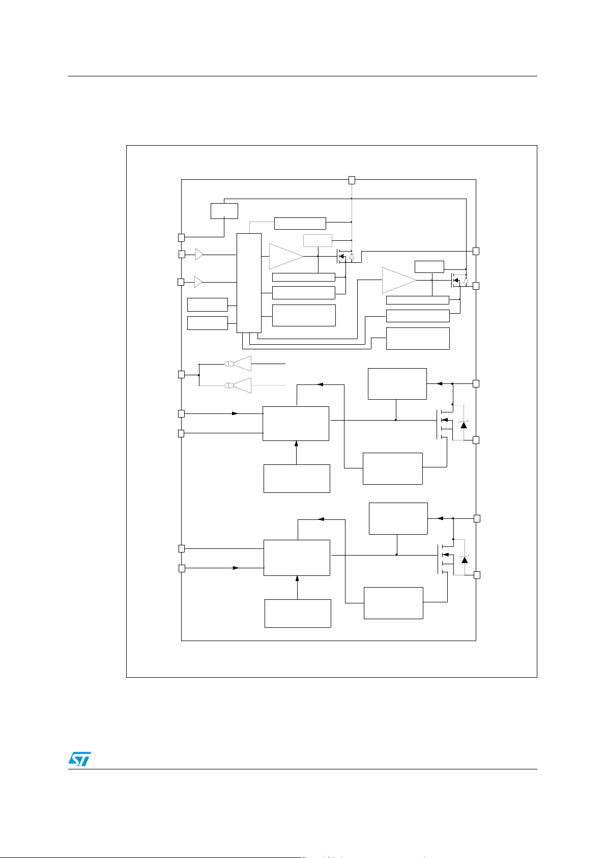
VN5772AK-E Block diagram and pin description
1 Block diagram and pin description
Figure 1. Block diagram
Vcc
Vcc
GND
INPUT1
INPUT2
C.SENSE
clamp
Logic
Overtemp. 1
Overtemp. 2
K
K
Undervoltage
Driver 1
Current limiter 1
Vds limiter 1
Power limitation
IDS1
IDS2
Clamp 1
Driver 2
Current limiter 2
VDS limiter 2
Power limitation
Overvoltage
Clamp
SOURCE1
Clamp 2
SOURCE2
DRAIN3
INPUT3
STATUS3
STATUS4
INPUT4
LOGIC
Over
Temperature
LOGIC
Over
Temperature
Linear
Current
Limiter
Overvoltage
Clamp
Linear
Current
Limiter
SOURCE3
DRAIN4
SOURCE4
Doc ID 16084 Rev 5 5/34

Block diagram and pin description VN5772AK-E
Table 2. Pin description
No pin Name Function
1, 3, 25, 28 DRAIN 3 Drain of switch 3 (low-side switches)
2 INPUT 3 Input of switch 3 (low-side switch)
4 STATUS 3 Status of switch 3 (low-side switch)
11 STATUS 4 Status of switch 4 (low-side switch)
5, 10, 19, 24 V
CC
6 GND Ground of switches 1 and 2 (high-side switches)
8 INPUT 1 Input of switch 1 (high-side switch)
7 INPUT 2 Input of switch 2 (high-side switch)
Drain of switches 1 and 2 (high-side switches) and power supply
voltage
9 C.SENSE
Analog current sense pin, delivers a current proportional to the load
current
12, 14, 15, 18 DRAIN 4 Drain of switch 4 (low-side switches)
13 INPUT 4 Input of switch 4 (low-side switch)
16, 17 SOURCE 4 Source of switch 4 (low-side switches)
22, 23 SOURCE 2 Source of switch 2 (high-side switches)
20, 21 SOURCE 1 Source of switch 1 (high-side switches)
26, 27 SOURCE 3 Source of switch 3 (low-side switches)
Figure 2. Configuration diagram (top view)
DRAIN 3
INPUT 3
DRAIN 3
STATUS 3
STATUS 3
V
CC
GND
INPUT 2
DRAIN 3
SOURCE 3
SOURCE 3
DRAIN 3
V
CC
SOURCE 2
SOURCE 2
INPUT 1
C.SENSE
V
CC
STATUS 4
STATUS 4
DRAIN 4
INPUT 4
DRAIN 4
6/34 Doc ID 16084 Rev 5
SOURCE 1
SOURCE 1
V
CC
DRAIN 4
SOURCE 4
SOURCE 4
DRAIN 4

VN5772AK-E Electrical specification
2 Electrical specification
2.1 Absolute maximum ratings
Stressing the device above the rating listed in the “absolute maximum ratings” table may
cause permanent damage to the device. These are stress ratings only and operation of the
device at these or any other conditions above those indicated in the operating sections of
this specification is not implied. Exposure to the conditions in the tables below for extended
periods may affect device reliability. Refer also to the STMicroelectronics SURE program
and other relevant quality document.
Table 3. Dual high-side switch
Symbol Parameter Value Unit
V
-V
- I
GND
I
OUT
- I
OUT
I
-I
CSENSE
V
CSENSE
E
MAX
V
ESD
V
ESD
T
T
DC supply voltage 41 V
CC
Reverse DC supply voltage 0.3 V
CC
DC reverse ground pin current 200 mA
DC output current Internally limited A
Reverse DC output current -12 A
DC input current -1 to 10 mA
IN
DC reverse C.SENSE pin current 200 mA
V
Current sense maximum voltage
CC
+V
Maximum switching energy (single pulse)
(L = 3 mH; RL=0Ω; V
= I
(Typ.)
I
OUT
limL
)
=13.5V; T
bat
jstart
= 150 °C;
104 mJ
Electrostatic discharge (human body model: R = 1.5 KΩ;
C = 100 pF)
– Input
– Current sense
– SOURCE
–V
CC
/DRAIN
n
n
4000
2000
5000
5000
Charge device model (CDM-AEC-Q100-011) 750 V
Junction operating temperature -40 to 150 °C
j
Storage temperature -55 to 150 °C
stg
- 41
CC
V
V
V
V
V
V
Doc ID 16084 Rev 5 7/34
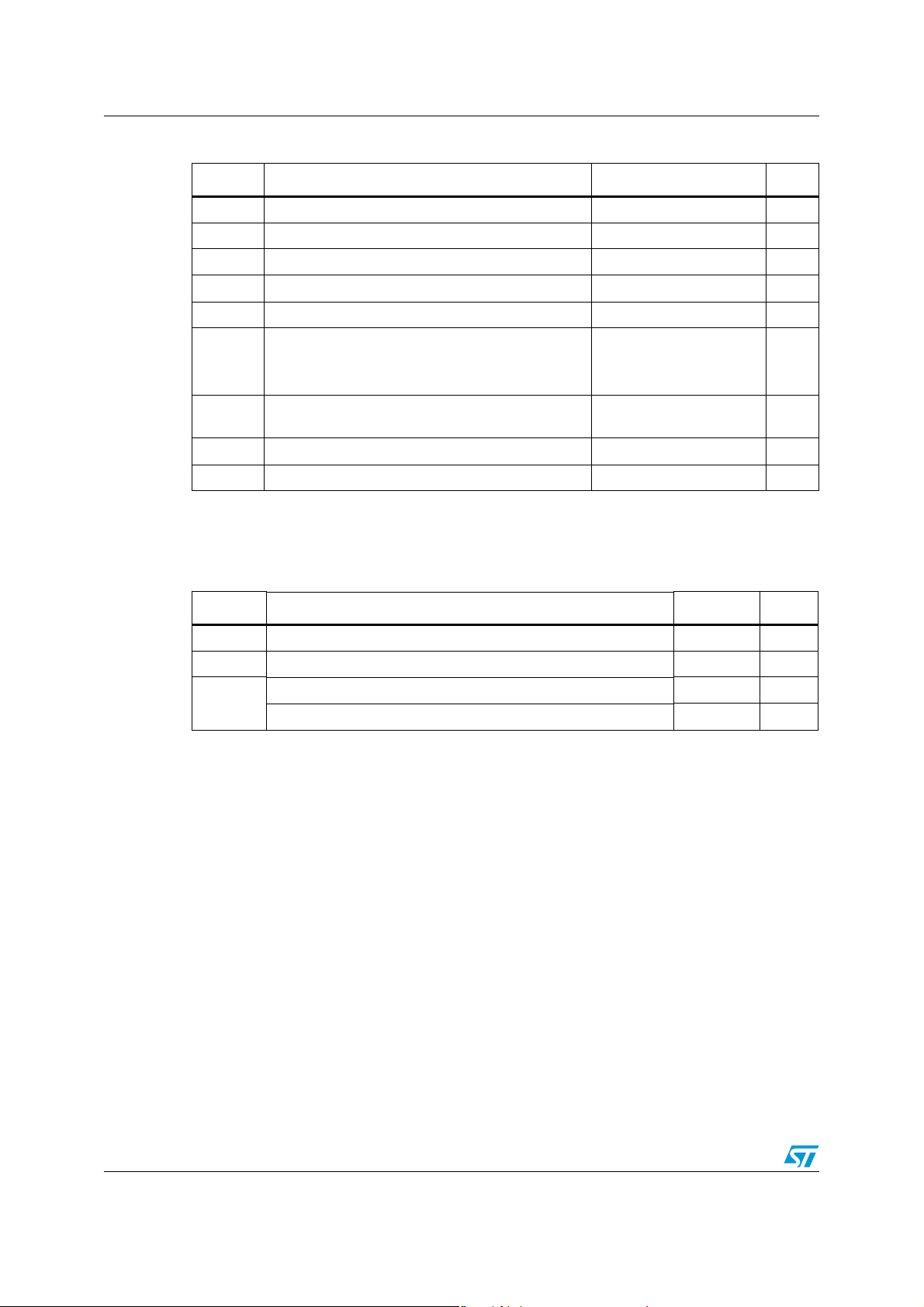
Electrical specification VN5772AK-E
Table 4. Low side switch
Symbol Parameter Value Unit
V
I
I
-I
I
STAT
DSn
INn
Drain-source voltage (V
Input current -1 to 10 mA
Drain current Internally limited A
Dn
Reverse DC output current -4 A
Dn
DC status current -1 to 10 mA
Electrostatic discharge (R = 1.5 KΩ, C = 100 pF):
V
ESD1
–Drain
– Supply, status, input
V
ESD2
T
Electrostatic discharge on output pins only
(R = 330 Ω, C = 150 pF)
Operating junction-temperature -40 to 150 °C
T
j
Storage temperature -55 to 150 °C
stg
2.2 Thermal data
Table 5. Thermal data
Symbol Parameter Max. value Unit
R
thj-leadHS
R
thj-leadLS
R
thj-amb
Thermal resistance junction-case (high-side switch) 22 °C/W
Thermal resistance junction-case (low-side switch) 21 °C/W
Thermal resistance junction-ambient (high-side switch) 47 °C/W
Thermal resistance junction-ambient (low-side switch) 57 °C/W
= 0 V) Internally clamped V
INn
5000
4000
2000 V
V
8/34 Doc ID 16084 Rev 5

VN5772AK-E Electrical specification
2.3 Electrical characteristics
2.3.1 Electrical characteristics for dual high-side switches
Values specified in this section are for 8 V < VCC<36V; -40°C<Tj< 150 °C, unless
otherwise specified (for each channel).
Table 6. Power section
Symbol Parameter Test conditions Min. Typ. Max. Unit
V
V
V
USDhyst
R
V
clamp
I
L(off)
1. PowerMOS leakage included.
2. For each channel.
Operating supply
CC
voltage
Undervoltage
USD
shutdown
Undervoltage
shutdown hysteresis
On-state resistance
ON
Voltage clamp IS = 20 mA 41 46 52 V
I
Supply current
S
Off-state output
(2)
current
Output - VCC diode
V
F
voltage
(2)
4.5 13 36 V
3.5 4.5 V
0.5 V
= 3 A; Tj = 25 °C 50
I
OUT
= 3 A; Tj = 150 °C 100
OUT
I
= 3 A; V
OUT
Off-state: V
V
IN=VOUT
On-state: V
=0A
I
OUT
VIN=V
OUT
=25°C
T
j
V
IN=VOUT
T
=125°C
j
I
= 3A, Tj = 150 °C 0.7 V
OUT
= 5 V; Tj = 25 °C 65
CC
= 13 V; Tj = 25 °C,
CC
= V
CC
=0V; VCC=13V,
=0V; VCC=13V,
= 0 V
SENSE
=13V; VIN=5V,
00.01 3
05
(1)
2
36mA
mΩI
(1)
5
µA
µA
Table 7. Switching (VCC = 13 V)
Symbol Parameter Test conditions Min. Typ. Max. Unit
t
d(on)
t
d(off)
(dV
/dt)onTurn-on voltage slope RL = 6.5 Ω —
OUT
(dV
OUT
/dt)
Turn-on delay time RL = 6.5 Ω (see
Turn-off delay time RL = 6.5 Ω (see
Turn-off voltage slope RL = 6.5 Ω —
off
Figure 4
Figure 4
)— 25 — µs
)— 20 — µs
See
Figure 15
See
Figure 17
—V/µs
—V/µs
Doc ID 16084 Rev 5 9/34
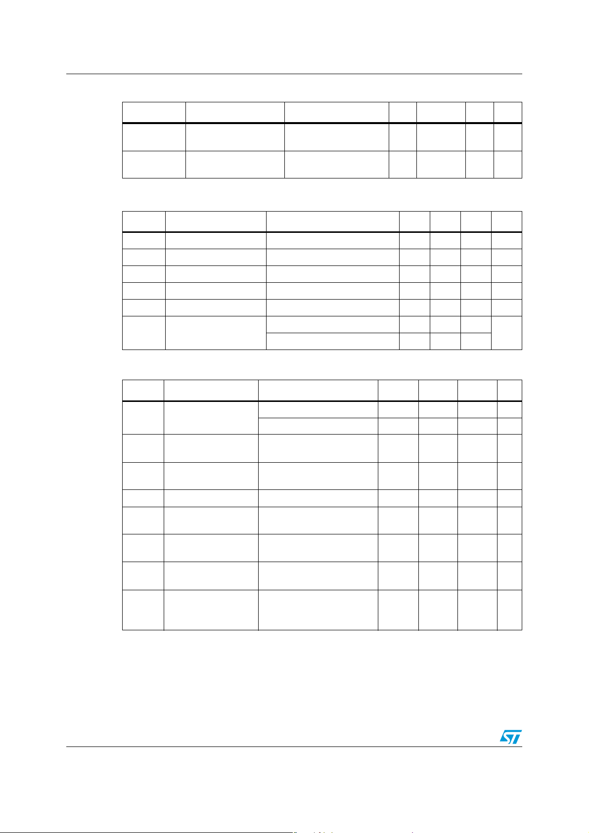
Electrical specification VN5772AK-E
Table 7. Switching (VCC = 13 V) (continued)
Symbol Parameter Test conditions Min. Typ. Max. Unit
W
ON
W
OFF
Table 8. Logic inputs
Switching energy
losses during t
won
Switching energy
losses during t
woff
RL = 6.5 Ω (see
RL = 6.5 Ω (see
Figure 4
Figure 4
)— 0.24 — mJ
)— 0.2 — mJ
Symbol Parameter Test conditions Min. Typ. Max. Unit
V
V
V
I(hyst)
V
Table 9. Protection and diagnostics
Low-level input voltage 0.9 V
IL
I
Low-level input current V
IL
High-level input voltage 2.1 V
IH
I
High-level input current V
IH
= 0.9 V 1 µA
IN
= 2.1 V 10 µA
IN
Input voltage hysteresis 0.25 V
I
= 1 mA 5.5 7
Input voltage clamp
ICL
IN
= -1 mA -0.7
I
IN
(1)
Symbol Parameter Test conditions Min. Typ. Max. Unit
V
= 13 V 12 18 24 A
I
limH
DC short-circuit
current
CC
5V<VCC<36V 24 A
V
I
T
T
T
HYST
V
DEMAG
V
1. To ensure long-term reliability under heavy overload or short-circuit conditions, protection and related
diagnostic signals must be used together with a proper software strategy. If the device is subjected to
abnormal conditions, this software must limit the duration and number of activation cycles.
Short-circuit current
limL
during thermal cycling
Shutdown
TSD
temperature
Reset temperature TRS + 1 TRS + 5 °C
T
R
Thermal reset of
RS
STATUS
Thermal hysteresis
(T
- TR)
TSD
Turn-off output voltage
clamp
Output voltage drop
ON
limitation
= 13 V; TR < Tj < T
V
CC
= 2 A; V
I
OUT
I
= 0.1 A,
OUT
= -40 °C to 150 °C
T
j
(see
Figure 5
IN
)
TSD
150 175 200 °C
135 °C
= 0; L = 6 mH VCC - 41 V
7A
7°C
CC
- 46 V
- 52 V
CC
25 mV
10/34 Doc ID 16084 Rev 5

VN5772AK-E Electrical specification
Table 10. Current sense (8 V < V
Symbol Parameter Test conditions Min. Typ. Max. Unit
K
K
K
K
I
OUT
I
OUT
I
OUT
I
OUT
/ I
/ I
/ I
/ I
SENSE
SENSE
SENSE
SENSE
0
1
2
3
< 16 V)
CC
I
= 0.35 A; V
OUT
SENSE
Tj = -40 °C to 50 °C
I
= 1 A; V
OUT
SENSE
Tj = -40 °C to 150 °C
Tj = 25 °C to 150 °C
I
= 2 A; V
OUT
SENSE
Tj = -40 °C to 150 °C
T
= 25 °C to 150 °C
j
I
= 6 A; V
OUT
T
= -40 °C to 150 °C
j
SENSE
Tj = 25 °C to 150 °C
= 0.5 V;
= 0.5 V;
= 4 V;
= 4 V;
1430 2140 2890
1470
2020
2610
1570
2020
2470
1740
2020
2320
1790
2020
2250
1890
2010
2140
1890
2010
2140
V
SENSE
I
SENSE0
V
SENSEH
I
SENSEH
t
DSENSE2H
t
DSENSE2L
Max analog sense output
voltage
Analog sense leakage
current
Analog sense output
voltage in overtemperature
condition
Analog sense output
current in overtemperature
condition
Delay response time from
rising edge of INPUT pin
Delay response time from
falling edge of INPUT pin
I
= 4 A; 5 V
OUT
= 0 A,
I
OUT
V
V
SENSE
= 0 V,
IN
= 0 V,
01
Tj = -40 °C to 150 °C
= 0 A,
I
OUT
V
V
T
V
V
V
0.5 A < I
I
(see
V
0.5 A < I
I
(see
= 0 V,
SENSE
= 5 V,
IN
= -40 °C to 150 °C
j
= 13 V, R
CC
= 13 V, V
CC
SENSE
SENSE
Figure 3
SENSE
SENSE
Figure 3
SENSE
SENSE
< 4 V,
< 4 A,
OUT
= 90% of I
)
< 4 V,
< 4 A,
OUT
= 10% of I
)
02
= 10 KΩ 9V
= 5 V 8 mA
80 250 µs
SENSE max
100 250 µs
SENSE max
µA
Doc ID 16084 Rev 5 11/34
 Loading...