

Features
VN340SP-33-E
Quad high side smart power solid state relay
Typ e V
VN340SP-33-E VCC-55 V 0.2 Ω 1 A 36 V
1. Per channel.
■ Output current: 1 A per channel
■ Digital I/O‘s clamped at 32 V minimum voltage
■ Shorted load and overtemperature protections
■ Protection against loss of ground
■ Built-in current limiter
■ Undervoltage shut-down
■ Open drain diagnostic output
■ Fast demagnetization of inductive loads
■ Conforms to IEC 61131-2
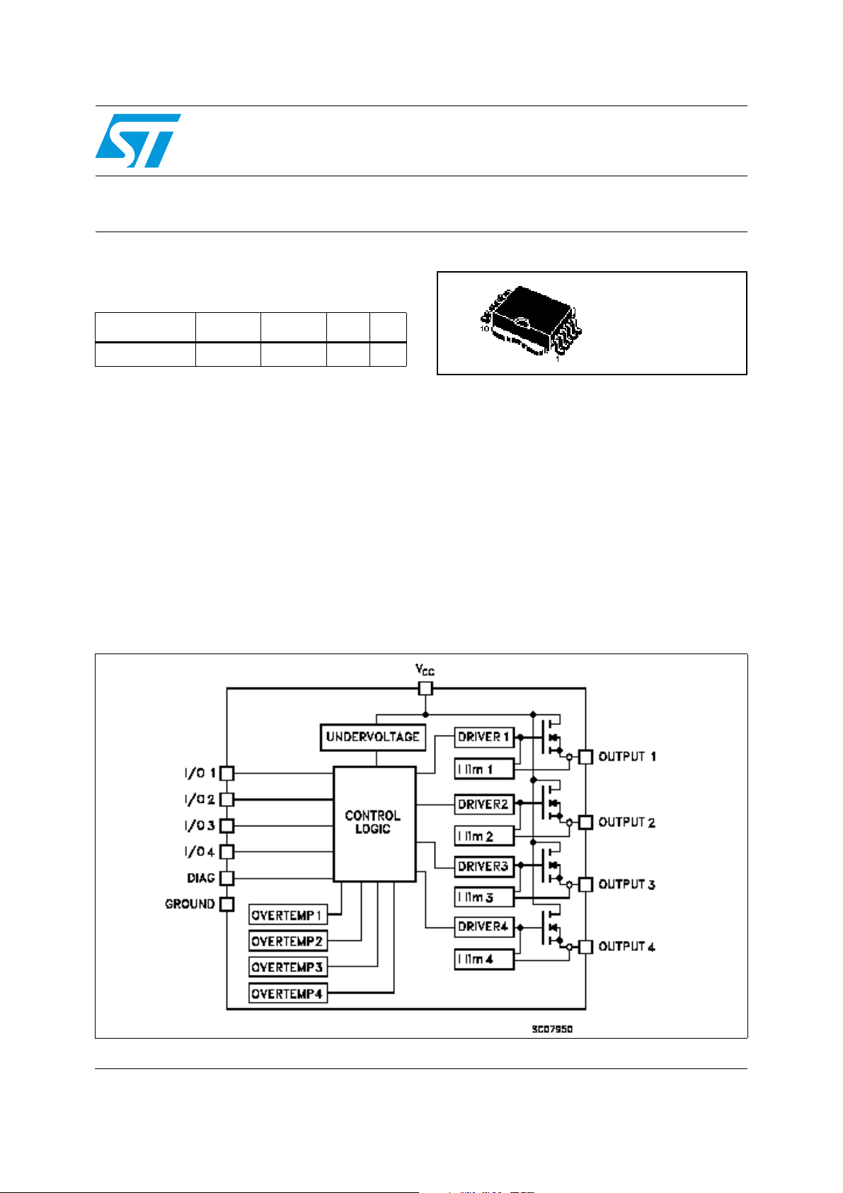
Figure 1. Block diagram
demag
(1)
R
DS(on)
(1)
I
out
(1)
V
CC
PowerSO-10
TM
Description
The VN340SP-33-E is a monolithic device made
using STMicroelectronics VIPower technology,
intended for driving four independent resistive or
inductive loads with one side connected to
ground. Active current limitation avoids dropping
the system power supply in case of shorted load.
Built-in thermal shut-down protects the chip from
overtemperature and short circuit. The open drain
diagnostic output indicates overtemperature
conditions. Each I/O is pulled down when
overtemperature condition of the relative channel
is verified.
August 2008 Rev 3 1/16
www.st.com
16

Contents VN340SP-33-E
Contents
1 Maximum ratings . . . . . . . . . . . . . . . . . . . . . . . . . . . . . . . . . . . . . . . . . . . . 3
2 Pin connections . . . . . . . . . . . . . . . . . . . . . . . . . . . . . . . . . . . . . . . . . . . . . 4
3 Electrical characteristics . . . . . . . . . . . . . . . . . . . . . . . . . . . . . . . . . . . . . 5
4 Test circuits . . . . . . . . . . . . . . . . . . . . . . . . . . . . . . . . . . . . . . . . . . . . . . . . 7
5 Switching time waveforms and truth table . . . . . . . . . . . . . . . . . . . . . . . 9
6 Package mechanical data . . . . . . . . . . . . . . . . . . . . . . . . . . . . . . . . . . . . 11
7 Order codes . . . . . . . . . . . . . . . . . . . . . . . . . . . . . . . . . . . . . . . . . . . . . . . 14
8 Revision history . . . . . . . . . . . . . . . . . . . . . . . . . . . . . . . . . . . . . . . . . . . 15
2/16
VN340SP-33-E Maximum ratings
1 Maximum ratings
Table 1. Absolute maximum rating
Symbol Parameter Values Unit
V
-V
I
OUT
I
I
DIAG
V
ESD
Power supply voltage 45 V
CC
Reverse supply voltage -4 V
CC
Output current (continuos) Internally limited A
I
Reverse output current (per channel) -6 A
R
Input current (per channel) ± 10 mA
IN
Diag pin current ± 10 mA
Electrostatic discharge (R = 1.5 kΩ; C = 100 pF) 2000 V
Single pulse avalanche energy per channel not
AS
simultaneously
400 mJ
E
Figure 4.
Power dissipation at Tc = 25 °C Internally limited w
tot
Junction operating temperature Internally limited °C
J
Storage temperature -55 to 150 °C
T
P
T
STG
Table 2. Thermal data
Symbol Parameter Values Unit
R
R
1. Per channel
2. When mounted using minimum recommended pad size on FR-4 board
Thermal resistance junction-case
thJC
Thermal resistance junction-ambient
thJA
(1)
(2)
Max 3 °C/W
Max 50 °C/W
3/16
Pin connections VN340SP-33-E
2 Pin connections
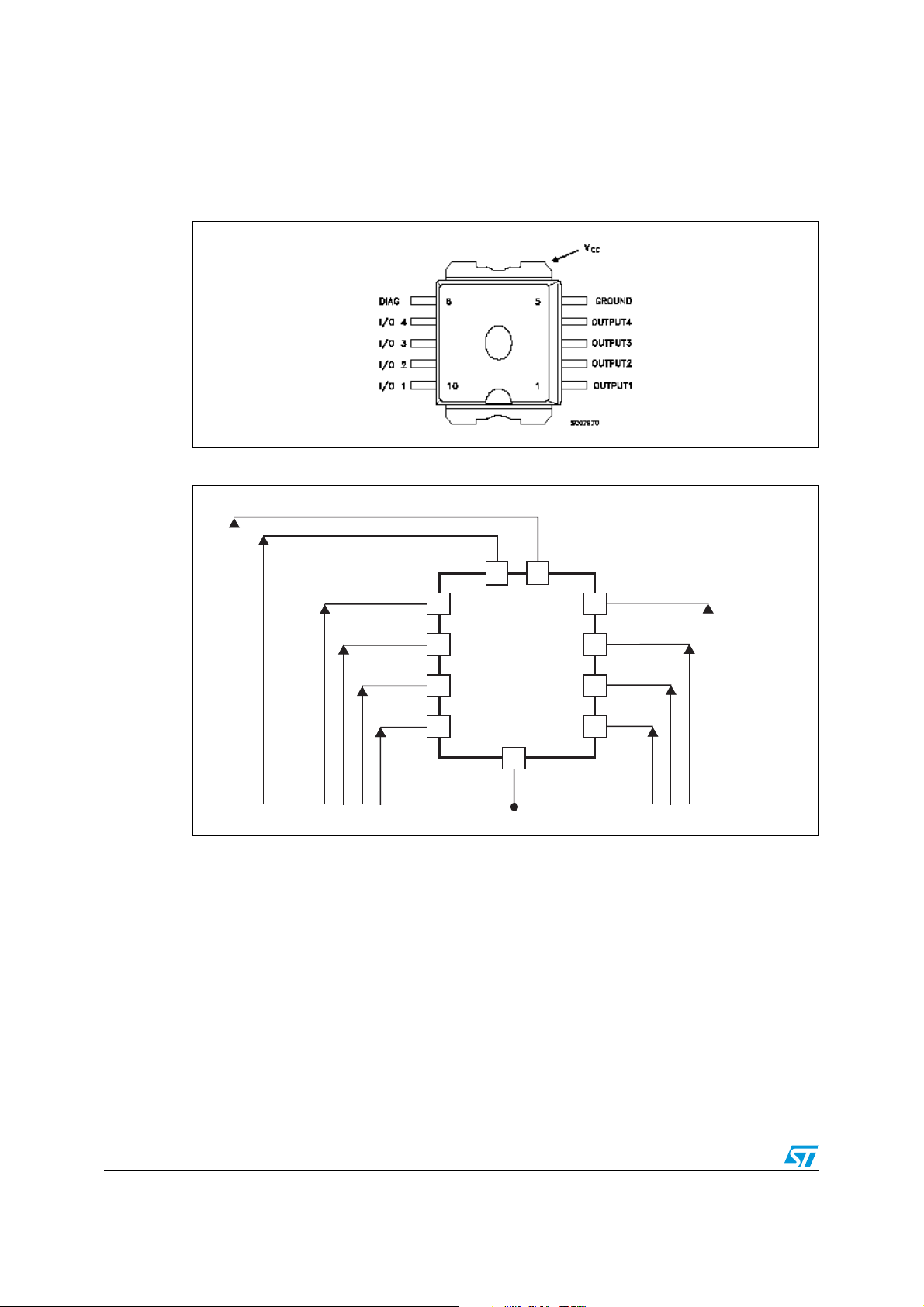
Figure 2. Connection diagram (top view)
Figure 3. Current and voltage conventions
VCC
VIN1
VIN2
VIN3
VIN4
IIN1
IIN2
IIN3
IIN4
IDIAG
VDIAG
9
8
7
6
IN2
IN3
IN4
DIAG
10
IN1
GND
V
CC
11
IOUT1
OUT1
OUT2
OUT3
OUT4
5
1
2
3
4
IOUT2
IOUT3
IOUT4
VOUT1
VOUT2
VOUT3
VOUT4
4/16
VN340SP-33-E Electrical characteristics
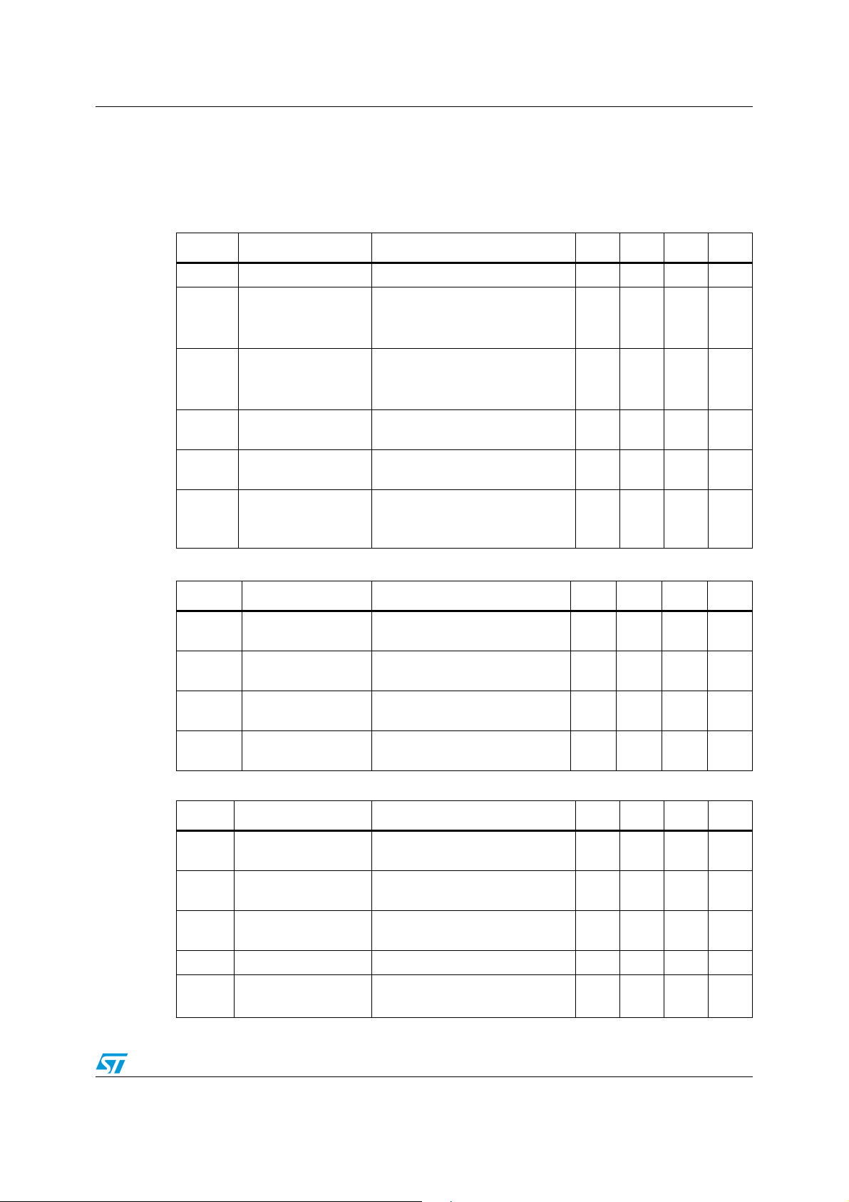
3 Electrical characteristics
10 V < V
Table 3. Power section
< 36 V; -40 °C < TJ < 125 °C; unless otherwise specified
CC
Symbol Parameter Test conditions Min Typ Max Unit
V
R
V
V
demag
I
LGND
Table 4. Switching (V
Supply voltage 10 36 V
CC
I
= 0.5 A; TJ = 25 °C
OUT
On state resistance
ON
I
= 0.5 A; TJ = 85 °C
OUT
= 0.5 A; TJ = 125 °C
I
OUT
All channels OFF
I
Supply current
S
Low state output
OL
voltage
Output voltage at
turn-off
Output current at
turn-off
CC
On state; V
= 125 °C)
(T
J
V
= VIL; R
IN
I
= 0.5 A; L
OUT
VCC = V
V
= 18 to 30 V
STAT
= - 25 °C to 85 °C Figure 6.
T
A
INn
= 30 V; I
IN
>= 10 MΩ 1.5 V
LOAD
LOAD
= V
GND
= 24 V)
OUT
>= 1 mH
=
= 0 V
-65VCC-55VCC-
V
CC
0.2
0.32
0.4
1
6
45
2mA
Symbol Parameter Test conditions Min Typ Max Unit
Ω
Ω
Ω
mA
mA
V
t
d(ON)
t
d(OFF)
Table 5. Logical input
Turn-on delay time of
Output current
Rise time of output
t
r
current
Turn-off delay time of
output current
Fall time of output
t
f
current
I
= 0.5 A, resistive load input
OUT
rise time < 0.1 μs, T
I
= 0.5 A, resistive load input
OUT
rise time < 0.1 μs, T
I
= 0.5 A, resistive load input
OUT
= 25 °C
J
= 25 °C
J
rise time < 0.1 μs, TJ = 25 °C
I
= 0.5 A, resistive load input
OUT
rise time < 0.1 μs, T
= 25 °C
J
52 100 μs
94 250 μs
34 50 μs
820μs
Symbol Parameter Test conditions Min Typ Max Unit
I/O input low level
V
IL
voltage
I/O input high level
V
IH
voltage
V
I(HYST)
V
1. The input voltage is internally clamped at 32 V minimum, it is possible to connect the input pins to an higher
I/O input hysteresis
voltage
I/O input current V
I
IN
I/O input clamp
ICL
voltage
voltage via an external resistor calculate to not exceed 10 mA
(1)
(1)
= 30 V 25 μΑ
IN
I
= 1 mA
IN
I
= -1 mA
IN
3.5 V
0.5 V
32 36
-0.7
2V
V
V
5/16
 Loading...