


VN16BSP
ISO HIGH SIDE SMART POWER SOLID STATE RELAY
Table 1. General Features
Typ e
VN16BPS 40 V 0.06 Ω 5.6 A 26 V
■ MAXIMUM CONTINUOUS OUTPUT
V
DSS
CURRENT: 20 A @ T
■ 5V LOGIC LEVEL COMPATIBLE INPUT
■ THERMAL SHUT-DOWN
■ UNDER VOLTAGE PROTECTION
■ OPEN DRAIN DIAGNOSTIC OUTPUT
■ INDUCTIVE LOAD FAST DEMAGNETIZATION
■ VERY LOW STAND-BY POWER
R
DS(on)
= 85°C
c
I
OUT
V
CC
DISSIPATION
DESCRIPTION
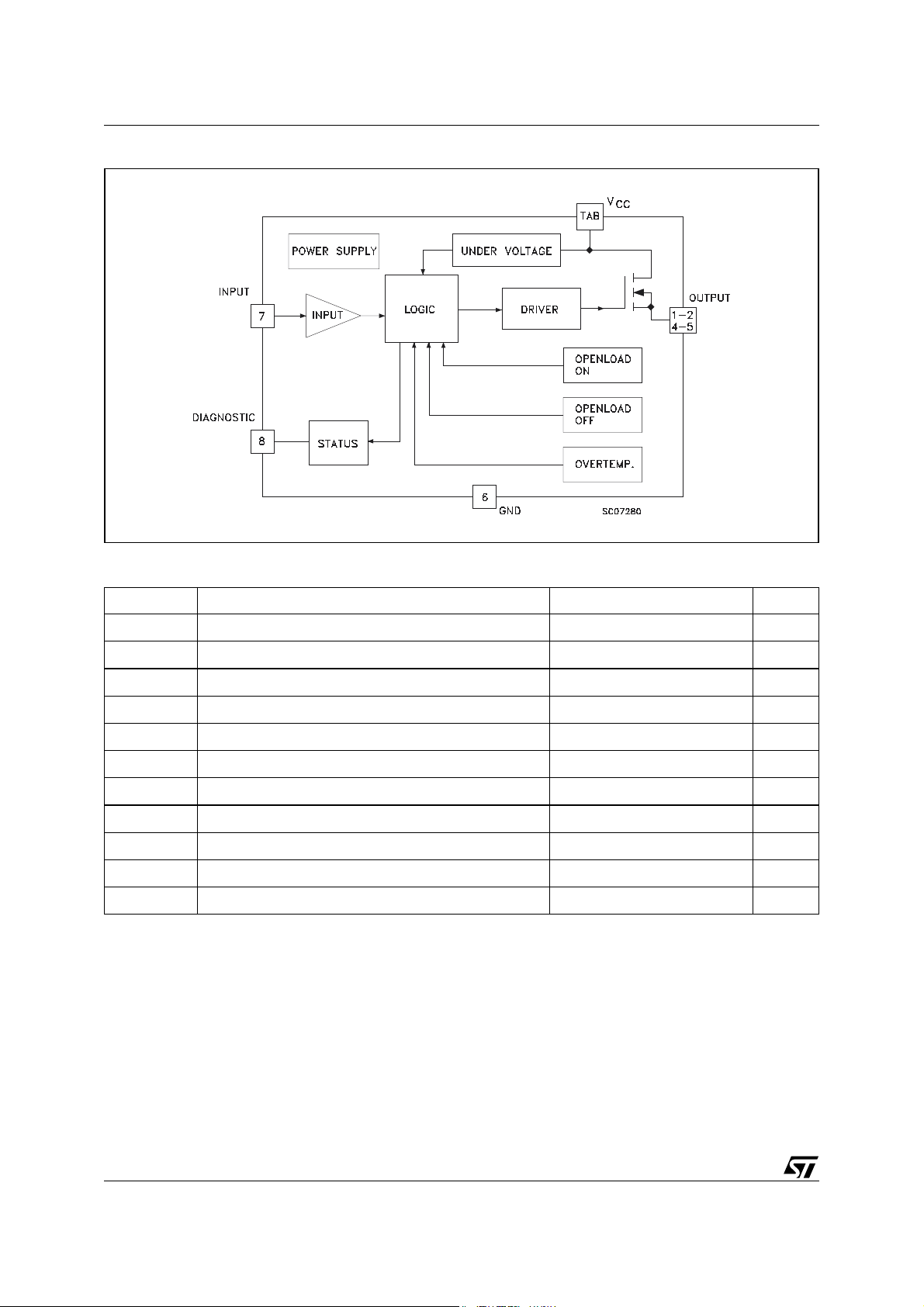
The VN16BPS is a monolithic device made using
STMicroelectronics VIPower Technology,
intended for driving resistive or inductive loads
with one side grounded.
Built-in thermal shut-down protects the chip from
over temperature and short circuit.
The open drain diagnostic output indicates: open
load in off state and in on state, output shorted to
and overtemperature. Fast demagnetization
V
CC
of inductive loads is achieved by negative (-18V)
load voltage at turn-off.
Figure 1. Package
10
1
PowerSO-10
Table 2. Order Codes
Package Tube Tape and Reel
PowerSO-10 VN16BSP VN16BSP13TR
REV. 2
1/11June 2004
VN16BSP
Figure 2. Block Diagram
Table 3. Absolute Maximum Ratings
Symbol Parameter Value Unit
I
OUT
V
Drain-Source Breakdown Voltage 40 V
(BR)DSS
I
OUT
Output Current (cont.) at Tc = 85 °C 20 A
(RMS) RMS Output Current at Tc = 85 °C 20 A
Reverse Output Current at Tc = 85 °C (f > 1Hz) –20 A
Input Current ±10 mA
Reverse Supply Voltage –4 V
Status Current ±10 mA
Electrostatic Discharge (1.5 kΩ, 100 pF) 2000 V
Power Dissipation at Tc = 25 °C 82 W
Junction Operating Temperature -40 to 150 °C
Storage Temperature -55 to 150 °C
– V
I
STAT
V
P
T
I
R
I
IN
CC
ESD
tot
T
j
stg
2/11
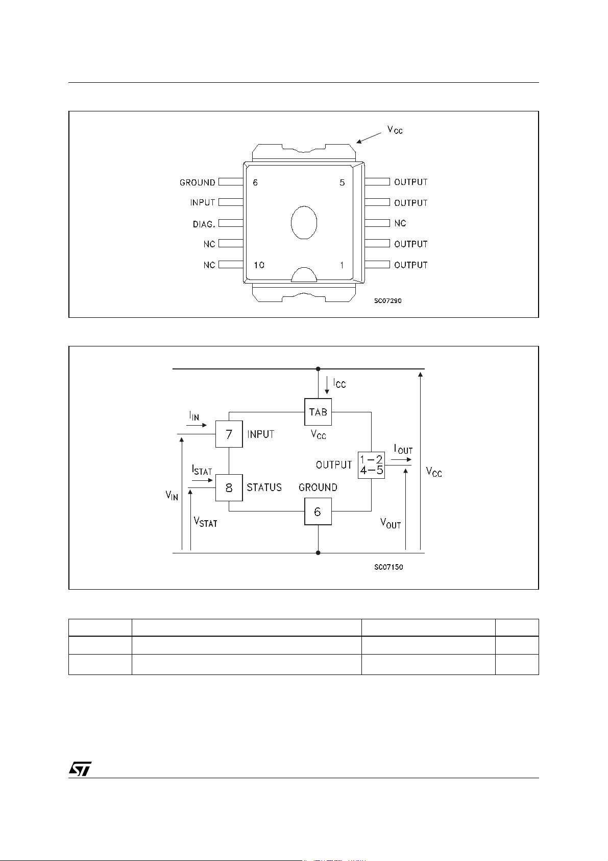
Figure 3. Connection Diagrams
Figure 4. Current and Voltage Conventions
VN16BSP
Table 4. Thermal Data
Symbol Parameter Value Unit
R
thj-case
R
thj-amb
Note: 1. When mounted using minimum recommended pad size on FR-4 board.
Thermal Resistance Junction-case Max 1.5 °C/W
Thermal Resistance Junction-ambient
(1)
Max
50 °C/W
3/11

VN16BSP
ELECTRICAL CHARACTERISTICS
(8 < V
Table 5. Power
Symbol Parameter Test Conditions Min. Typ. Max. Unit
V
Note: 2. In= Nominal current according to ISO definition for high side automotive switch. The Nominal Current is the current at Tc = 85 °C
Table 6. Switching
Symbol Parameter Test Conditions Min. Typ. Max. Unit
(di/dt)
(di/dt)
Note: 3. See Switching Time Waveforms.
< 16 V; -40 ≤ Tj ≤ 125 °C unless otherwise specified)
CC
V
I
n
R
I
DS(MAX)
R
Supply Voltage 6 13 26 V
CC
(2)
Nominal Current Tc = 85 °C; V
On State Resistance I
on
Supply Current Off State; V
S
Maximum Voltage Drop I
Output to GND Internal
j
= In; V
OUT
= 20 A; V
OUT
Tj = 25 °C 5 10 20 KΩ
Impedance
for battery voltage of 13V which produces a voltage drop of 0.5 V.
(3)
t
d(on)
t
t
d(off)
t
V
demag
Turn-on Delay Time Of
Output Current
(3)
r
Rise Time Of Output
Current
(3)
Turn-off Delay Time Of
Output Current
(3)
f
Fall Time Of Output
Current
Turn-on Current Slope R
on
Turn-off Current Slope R
off
Inductive Load Clamp
R
= 1.6 Ω 5 50 500 µs
load
R
= 1.6 Ω 40 100 680 µs
load
R
= 1.6 Ω 10 100 500 µs
load
R
= 1.6 Ω 40 100 680 µs
load
= 1.6 Ω; V
load
= 1.6 Ω; V
load
R
= 1.6 Ω; L = 1 mH –24 –18 –14 V
load
Voltage
≤ 0.5; V
DS(on)
= 13 V; Tj = 25 °C 0.038 0.06 Ω
CC
= 13 V; Tj ≥ 25 °C 25 50 µA
CC
= 13 V; Tc = 85 °C 1 1.8 V
CC
= 13 V 0.008 0.1 A/µs
CC
= 13 V 0.008 0.1 A/µs
CC
= 13 V 5.6 8.8 A
CC
Table 7. Logic Input
Symbol Parameter Test Conditions Min. Typ. Max. Unit
V
V
V
I(hyst)
I
IN
V
ICL
Note: 4. The VIH is internally clamped at 6V about. It is possible to connect this pin to an higher voltage via an external resistor calculated
4/11
Input Low Level Voltage 1.5 V
IL
Input High Level Voltage 3.5 Note 4 V
IH
Input Hysteresis Voltage 0.2 1 1.5 V
Input Current VIN = 5 V; Tj = 25 °C 100 µA
Input Clamp Voltage IIN = 10 mA
to not exceed 10 mA at the input pin.
= –10 mA
I
IN
56
–0.7
7V
V
 Loading...