

Features
VN03
ISO high side smart power solid state relay
Typ e V
DSS
R
DS(on)
(1)
I
n
V
CC
VN03 60 V 0.5 Ω 0.7 A 26 V
1. In= nominal current according to ISO definition for high
side automotive switch.
■ Maximum continuous output current
T
c= 25°C
■ 5V logic level compatible input
■ Thermal shutdown
■ Under voltage protection
■ Open drain diagnostic output
■ Inductive load fast demagnetization
■ Very low standby power dissipation
a. The maximum continuous output current is the current at
c = 85 °C for a battery voltage of 13V which does not activate
T
self protection.
(a)
: 4A @
PENTAWATT
Description
The VN03 is a monolithic device made using
STMicroelectronics Vertical Intelligent Power
technology, intended for driving resistive or
inductive loads with one side grounded. Built-in
thermal shutdown protects the chip from over
temperature and short circuit. The open Drain
diagnostic output indicates: open load in off state
and in on state, output shorted to V
overtemperature. Fast demagnetization of
inductive loads is archieved by negative (-18V)
load voltage at turn-off.
CC
and
Table 1. Device summary
Package Order codes
PENTAWATT VN03
November 2008 Rev 2 1/17
www.st.com
17

Contents VN03
Contents
1 Block diagram and pin description . . . . . . . . . . . . . . . . . . . . . . . . . . . . . 5
2 Electrical specifications . . . . . . . . . . . . . . . . . . . . . . . . . . . . . . . . . . . . . . 6
2.1 Absolute maximum ratings . . . . . . . . . . . . . . . . . . . . . . . . . . . . . . . . . . . . . 6
2.2 Thermal data . . . . . . . . . . . . . . . . . . . . . . . . . . . . . . . . . . . . . . . . . . . . . . . 7
2.3 Electrical characteristics . . . . . . . . . . . . . . . . . . . . . . . . . . . . . . . . . . . . . . . 7
3 Application information . . . . . . . . . . . . . . . . . . . . . . . . . . . . . . . . . . . . . 12
3.1 Functional description . . . . . . . . . . . . . . . . . . . . . . . . . . . . . . . . . . . . . . . 13
3.2 Protecting the device agaist load dump - test pulse 5 . . . . . . . . . . . . . . . 13
3.3 Protecting the device against reverse battery . . . . . . . . . . . . . . . . . . . . . 13
4 Package and packing information . . . . . . . . . . . . . . . . . . . . . . . . . . . . . 14
4.1 ECOPACK® packages . . . . . . . . . . . . . . . . . . . . . . . . . . . . . . . . . . . . . . . 14
4.2 PENTAWATT mechanical data . . . . . . . . . . . . . . . . . . . . . . . . . . . . . . . . . 14
5 Revision history . . . . . . . . . . . . . . . . . . . . . . . . . . . . . . . . . . . . . . . . . . . 16
2/17

VN03 List of tables
List of tables
Table 1. Device summary . . . . . . . . . . . . . . . . . . . . . . . . . . . . . . . . . . . . . . . . . . . . . . . . . . . . . . . . . . 1
Table 2. Absolute maximum ratings . . . . . . . . . . . . . . . . . . . . . . . . . . . . . . . . . . . . . . . . . . . . . . . . . . 6
Table 3. Thermal data. . . . . . . . . . . . . . . . . . . . . . . . . . . . . . . . . . . . . . . . . . . . . . . . . . . . . . . . . . . . . 7
Table 4. Power . . . . . . . . . . . . . . . . . . . . . . . . . . . . . . . . . . . . . . . . . . . . . . . . . . . . . . . . . . . . . . . . . . 7
Table 5. Switching (V
Table 6. Logic inputs. . . . . . . . . . . . . . . . . . . . . . . . . . . . . . . . . . . . . . . . . . . . . . . . . . . . . . . . . . . . . . 8
Table 7. Protections and diagnostics . . . . . . . . . . . . . . . . . . . . . . . . . . . . . . . . . . . . . . . . . . . . . . . . . 8
Table 8. Truth table. . . . . . . . . . . . . . . . . . . . . . . . . . . . . . . . . . . . . . . . . . . . . . . . . . . . . . . . . . . . . . 10
Table 9. PENTAWATT mechanical data . . . . . . . . . . . . . . . . . . . . . . . . . . . . . . . . . . . . . . . . . . . . . 15
Table 10. Document revision history . . . . . . . . . . . . . . . . . . . . . . . . . . . . . . . . . . . . . . . . . . . . . . . . . 16
=13V) . . . . . . . . . . . . . . . . . . . . . . . . . . . . . . . . . . . . . . . . . . . . . . . . . . . . . . 7
CC
3/17

List of figures VN03
List of figures
Figure 1. Block diagram . . . . . . . . . . . . . . . . . . . . . . . . . . . . . . . . . . . . . . . . . . . . . . . . . . . . . . . . . . . . 5
Figure 2. Configuration diagram (top view) . . . . . . . . . . . . . . . . . . . . . . . . . . . . . . . . . . . . . . . . . . . . . 5
Figure 3. Current and voltage conventions . . . . . . . . . . . . . . . . . . . . . . . . . . . . . . . . . . . . . . . . . . . . . 6
Figure 4. I
Figure 5. t
Figure 6. Switching time waveforms . . . . . . . . . . . . . . . . . . . . . . . . . . . . . . . . . . . . . . . . . . . . . . . . . 10
Figure 7. Waveforms . . . . . . . . . . . . . . . . . . . . . . . . . . . . . . . . . . . . . . . . . . . . . . . . . . . . . . . . . . . . . 11
Figure 8. Over current test circuit. . . . . . . . . . . . . . . . . . . . . . . . . . . . . . . . . . . . . . . . . . . . . . . . . . . . 11
Figure 9. Typical application circuit with a schottky diode for reverse supply protection . . . . . . . . . . 12
Figure 10. Typical application circuit with separate signal ground . . . . . . . . . . . . . . . . . . . . . . . . . . . . 12
Figure 11. PENTAWATT package dimensions . . . . . . . . . . . . . . . . . . . . . . . . . . . . . . . . . . . . . . . . . . 14
test circuit. . . . . . . . . . . . . . . . . . . . . . . . . . . . . . . . . . . . . . . . . . . . . . . . . . . . . . . . . . 9
OL(off)
, t
povl
ISO definition . . . . . . . . . . . . . . . . . . . . . . . . . . . . . . . . . . . . . . . . . . . . . . . . . . . . . 9
pol
4/17
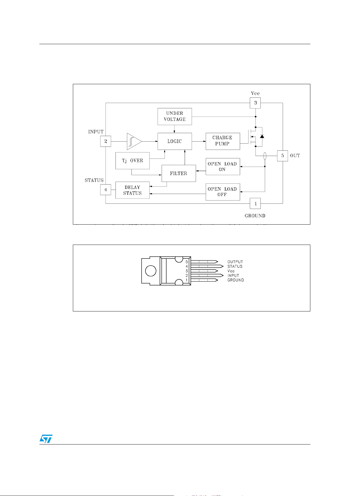
VN03 Block diagram and pin description
1 Block diagram and pin description
Figure 1. Block diagram
Figure 2. Configuration diagram (top view)
PENTAWATT
5/17
Electrical specifications VN03
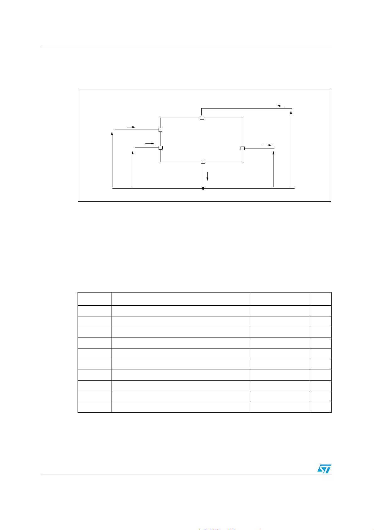
2 Electrical specifications
Figure 3. Current and voltage conventions
I
CC
I
IN
INPUT
I
STAT
STATUS
V
IN
V
STAT
2.1 Absolute maximum ratings
V
CC
GND
OUTPUT
I
GND
I
OUT
V
OUT
V
CC
Stressing the device above the rating listed in the “Absolute maximum ratings” table may
cause permanent damage to the device. These are stress ratings only and operation of the
device at these or any other conditions above those indicated in the operating sections of
this specification is not implied. Exposure to Absolute maximum rating conditions for
extended periods may affect device reliability. Refer also to the STMicroelectronics sure
program and other relevant quality document.
Table 2. Absolute maximum ratings
Symbol Parameter Value Unit
V
Drain-Source breakdown voltage 60 V
(BR)DSS
Output current (cont.) at Tc = 85°C 4 A
I
OUT
I
Reverse output current at Tc = 85°C -4 A
R
Input current ±10 mA
Reverse supply voltage -4 V
CC
Status current ±10 mA
Electrostatic discharge (1.5 kΩ, 100 pF) 2000 V
Power dissipation at Tc = 85°C 14 W
tot
Junction operating temperature -40 to 150 °C
j
-V
I
STAT
V
P
I
IN
ESD
T
Tstg Storage temperature -55 to 150 °C
6/17
 Loading...