

VL5510
High dynamic range CMOS sensor
Data Brief
Features
■ 1024 x 512 monochrome resolution sensor
■ High dynamic pixel (5.6 µm x 5.6 µm)
■ Parallel video data output interface (12 bit
parallel interface)
■ High speed serial link (CCP interface)
2
■ I
C control interface
■ SPI slave control interface
■ UART control interface
■ SPI master interface
■ 3.3 V operation, 2.5 V for LVDS pads power
supply
■ On board 12 bit ADC
■ Small physical size
■ Ultra low power standby mode
■ On chip PLL
■ 34 fps maximum frame rate at full resolution
■ On chip Anti Dark Sun correction
■ On chip VFPN correction (CDS)
■ On chip defect correction
■ On chip microcontroller for system level
flexibility
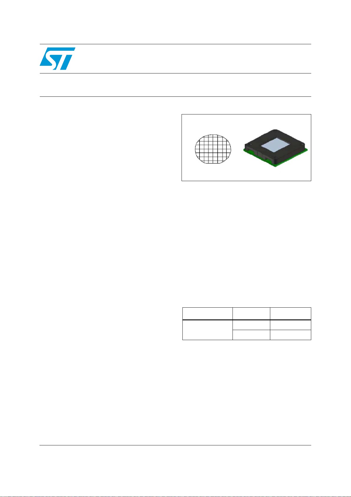
Bare die
Bare Die
OLGA
Applications
■ Adaptive cruise control/stop and go
■ Pedestrian detection and protection
■ Headway/forward collision warning
■ Pre-crash active safety
■ Lane departure warning
■ Lane keeping
■ Night vision (NIR - Near InfraRed)
■ Automatic high/low beam control
■ Lane change assist
■ Blind spot detection
Table 1. Device summary
Part number Package Packing
VL5510
Bare die Tray
OLGA UNSAW DICE
October 2008 Rev 2 1/8
For further information contact your local STMicroelectronics sales office.
www.st.com
1

Contents VL5510
Contents
1 Overview . . . . . . . . . . . . . . . . . . . . . . . . . . . . . . . . . . . . . . . . . . . . . . . . . . 3
1.1 Technical specifications . . . . . . . . . . . . . . . . . . . . . . . . . . . . . . . . . . . . . . . 3
1.2 Description . . . . . . . . . . . . . . . . . . . . . . . . . . . . . . . . . . . . . . . . . . . . . . . . . 4
2 Functional description . . . . . . . . . . . . . . . . . . . . . . . . . . . . . . . . . . . . . . . 5
3 Revision history . . . . . . . . . . . . . . . . . . . . . . . . . . . . . . . . . . . . . . . . . . . . 7
2/8

VL5510 Overview
1 Overview
1.1 Technical specifications
Table 2. Technical specifications
Pixel resolution 1024 x 512
Sensor technology 0.13 µm 4 layers metal
Pixel size 5.6 µm x 5.6 µm
Characteristic line 10 knee points
Analog gain +24 dB (max)
Dynamic range (in scene) 120 dB
Dynamic range (overall) 140 dB
Signal to noise TBD dB (@ 100 lux)
Minimum illumination < TBD lux
Supply voltage
3.3 V (±10 %) supply
2.5 V (±10 %) LVDS I/O supply
Power consumption
Temperature range
Shutter Electrical rolling
Pixel fill factor > 40 %
Remaining fixed pattern noise (FPN) < 0.1 %
Temporal noise < 0.1 %
Image lag < 0.1 %
Defect pixels To be specified
Package Bare die/OLGA
< 150 mW @ 34 fps
< 15 µW (standby mode)
-40 °C to + 125 °C
Device functional @ 85 °C max
3/8

Overview VL5510
1.2 Description
The VL5510 is a 0.13 µm CMOS digital camera featuring a high dynamic range (1024 x 512
resolution) for automotive applications. This complete camera module is ready to connect to
the camera enabled baseband processor.
Video data is output from the VL5510 over a 12-bit parallel interface and a high speed serial
link (8/10/12 bits raw data output format supported on the compact camera port (CCP)
interface compatible with an SMIA (standard mobile imaging architecture) normative.
Control interface is an SPI (serial peripheral interface) or UART (universal asynchronous
receiver transmitter) interface or I
2
C (Inter Integrated Circuit) interface.
Power supplies delivered to the sensor are:
● 3.3 V for the analog blocks,
● 3.3 V for the digital interface,
● 2.5 V for the high speed serial link interface,
● 1.2 V for the internal digital core (generated internally using a low drop output
regulator).
The VL5510 is designed to operate in conjunction with an electronic central unit (ECU) that
manages the device in the car.
An input clock is required in the range 6 MHz to 27.77 MHz.
The device contains an embedded video processor and delivers monochrome processed
images at up to 34 frames per second. The video processor integrates a wide range of
image enhancement functions, designed to ensure high image quality. These include:
● Antidark sun correction
● Dark calibration
● Vertical fix pattern correction
● Frame crop
● Defect pixel correction
● Test patterns generation
● Statistics generation (histogram)
● Sensor status data embedding (SCL, trailer)
S
4/8

VL5510 Functional description
2 Functional description
The block diagram of the VL5510 is shown in Figure 1. VL5510 includes the following main
blocks:
● Internal host (eWARP microcontroller): This is the internal host which is responsible for
system operation sequencing and image data processing. It has the following features:
– Safe system startup from hardware standby to software standby
– System boot to drive it from software standby to streaming mode
– System streaming soft stop
– Device reinitialization to default mode (software reset)
– High Dynamic mode setting (take in charge the management of the hardware
knee point setting).
● ICB: Imager control block which contains all communication interfaces, transaction
routings and resets and clock management
● IDP: Imager data pipeline which is responsible for real-time data processing at pixel
clock rate. It implements a set of correction algorithms and dedicated block-IPs for data
coding.
● CAB: Custom analog macro which contains the pixel array and all analog components
that allow it to be driven.
● Data transmitters: Video data coders and transmitters, including serial and parallel
interface.
5/8

Functional description VL5510
Figure 1. VL5510 block diagram
27 MHz crystal
CAB
Pixel array
1024 x 512
On chip
regulator
On chip osc
PLL
IDP
Video Timing
ROM
RAM
System
Clock
Gen
clocks
Video processing pipe
ICB_bank
IDP_bank
eWARP
(m8051)
arbitrer
decoder
SLC +Trailer
I2C slave IF
SPI/UART
slave IF
SPI master IF
CCP Tx
Parallel Tx
ICB
I2C
SPI/UART
slave
SPI
LV DS
OUT
DOUT
On chip
POR
UIA interface
RAM
LUT
6/8

VL5510 Revision history
3 Revision history
Table 3. Document revision history
Date Revision Changes
19-Jun-2007 1 Initial release.
Changed data in Table 2: Technical specifications
13-Oct-2008 2
Updated information in Section 1.2: Description
Updated information inSection 2: Functional description
7/8

VL5510
Please Read Carefully:
Information in this document is provided solely in connection with ST products. STMicroelectronics NV and its subsidiaries (“ST”) reserve the
right to make changes, corrections, modifications or improvements, to this document, and the products and services described herein at any
time, without notice.
All ST products are sold pursuant to ST’s terms and conditions of sale.
Purchasers are solely responsible for the choice, selection and use of the ST products and services described herein, and ST assumes no
liability whatsoever relating to the choice, selection or use of the ST products and services described herein.
No license, express or implied, by estoppel or otherwise, to any intellectual property rights is granted under this document. If any part of this
document refers to any third party products or services it shall not be deemed a license grant by ST for the use of such third party products
or services, or any intellectual property contained therein or considered as a warranty covering the use in any manner whatsoever of such
third party products or services or any intellectual property contained therein.
UNLESS OTHERWISE SET FORTH IN ST’S TERMS AND CONDITIONS OF SALE ST DISCLAIMS ANY EXPRESS OR IMPLIED
WARRANTY WITH RESPECT TO THE USE AND/OR SALE OF ST PRODUCTS INCLUDING WITHOUT LIMITATION IMPLIED
WARRANTIES OF MERCHANTABILITY, FITNESS FOR A PARTICULAR PURPOSE (AND THEIR EQUIVALENTS UNDER THE LAWS
OF ANY JURISDICTION), OR INFRINGEMENT OF ANY PATENT, COPYRIGHT OR OTHER INTELLECTUAL PROPERTY RIGHT.
UNLESS EXPRESSLY APPROVED IN WRITING BY AN AUTHORIZED ST REPRESENTATIVE, ST PRODUCTS ARE NOT
RECOMMENDED, AUTHORIZED OR WARRANTED FOR USE IN MILITARY, AIR CRAFT, SPACE, LIFE SAVING, OR LIFE SUSTAINING
APPLICATIONS, NOR IN PRODUCTS OR SYSTEMS WHERE FAILURE OR MALFUNCTION MAY RESULT IN PERSONAL INJURY,
DEATH, OR SEVERE PROPERTY OR ENVIRONMENTAL DAMAGE. ST PRODUCTS WHICH ARE NOT SPECIFIED AS "AUTOMOTIVE
GRADE" MAY ONLY BE USED IN AUTOMOTIVE APPLICATIONS AT USER’S OWN RISK.
Resale of ST products with provisions different from the statements and/or technical features set forth in this document shall immediately void
any warranty granted by ST for the ST product or service described herein and shall not create or extend in any manner whatsoever, any
liability of ST.
ST and the ST logo are trademarks or registered trademarks of ST in various countries.
Information in this document supersedes and replaces all information previously supplied.
The ST logo is a registered trademark of STMicroelectronics. All other names are the property of their respective owners.
© 2008 STMicroelectronics - All rights reserved
STMicroelectronics group of companies
Australia - Belgium - Brazil - Canada - China - Czech Republic - Finland - France - Germany - Hong Kong - India - Israel - Italy - Japan -
Malaysia - Malta - Morocco - Singapore - Spain - Sweden - Switzerland - United Kingdom - United States of America
www.st.com
8/8
 Loading...