

General Features
1
1
F
C
0
0
2
1
VIPer50A-E
VIPer50ASP-E
SMPS PRIMARY I.C.
Type
V
DSS
I
R
n
DS(on)
VIPer50A-E/ASP-E 700V 1.5A 5.7Ω
■ ADJUSTABLE SWITCHING FREQUENCY UP
TO 200 kHz
■ CURRENT MODE CONTROL
■ SOFT START AND SHUTDOWN CONTROL
■ AUTOMATIC BURST MODE OPERATION IN
STAND-BY CONDI T ION ABLE TO MEET
“BLUE ANGEL” NORM (<1w TOTAL POWER
CONSUMPTION)
■ INTERNALLY TRIMMED ZENER
REFERENCE
■ UNDERVOLTAGE LOCK-OUT WITH
HYSTERESIS
■ INTEGRATED START-UP SUPPLY
■ OVER-TEMPERATURE PROTECTION
■ LOW STAND-BY CURRENT
■ ADJUSTABLE CURRENT LIMITATION
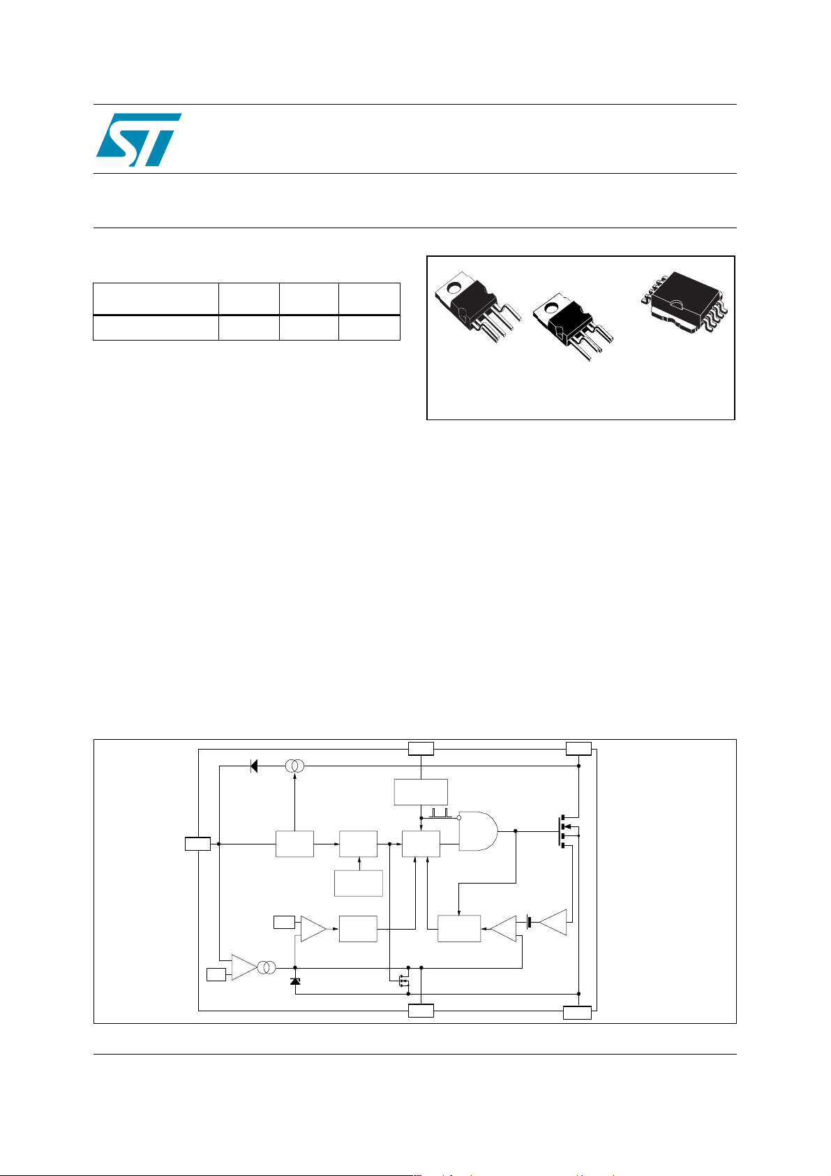
Block Diagr am
0
PENTAWATT HV
POWERSO-10
PENTAWATT HV (022Y)
Description
VIPer50A-E/ASP-E, made using VIPower M0
Technology, combines on the same silicon chip a
state-of-the-art PWM circuit together with an
optimized, high voltage, Vertical Power MOSFET
(700V/ 1.5A).
Typical applications cover offline power supplies
with a secondary power capability of 25W in wide
range condition and 50W in single ran ge or with
doubler configuration. It is compatible from both
primary or secondary regulation loop despite
using around 50% less components when
compared with a discrete solution. Burst mode
operation is an additional feature of this device,
offering the ability to operate in stand-by mode
without extra components.
OSC
DRAIN
TM
ON/OFF
SECURITY
LATCH
0.5 V
ERROR
AMPLIFIER
UVLO
LOGIC
+
_
4.5 V
R/S
OVERTEMP.
DETECTOR
1.7 µs
DELAY
V
DD
_
13 V
+
FF
QSR1
S
OSCILLATOR
PWM
LATCH
FF
R2 R3
COMP
Q
250 ns
BLANKING
+
_
0.5V
_
+
CURRENT
AMPLIFIER
2 V/A
9
SOURCE
Rev 1
September 2005 1/31
www.st.com
31

VIPer50A-E/ASP-E
Contents
1 Electrical Data . . . . . . . . . . . . . . . . . . . . . . . . . . . . . . . . . . . . . . . . . . . . . . . . 4
1.1 Maximum Rating . . . . . . . . . . . . . . . . . . . . . . . . . . . . . . . . . . . . . . . . . . . . . . . 4
1.2 Electrical Characteristics . . . . . . . . . . . . . . . . . . . . . . . . . . . . . . . . . . . . . . . . . 5
2 Thermal Data . . . . . . . . . . . . . . . . . . . . . . . . . . . . . . . . . . . . . . . . . . . . . . . . . 7
3 Pin Description . . . . . . . . . . . . . . . . . . . . . . . . . . . . . . . . . . . . . . . . . . . . . . . 8
3.1 Drain Pin (Integrated Power MOSFET Drain): . . . . . . . . . . . . . . . . . . . . . . . . 8
3.2 Source Pin: . . . . . . . . . . . . . . . . . . . . . . . . . . . . . . . . . . . . . . . . . . . . . . . . . . . 8
3.3 V
3.4 Compensation Pin . . . . . . . . . . . . . . . . . . . . . . . . . . . . . . . . . . . . . . . . . . . . . . 8
3.5 OSC Pin (Oscillat or Freque nc y ): . . . . . . . . . . . . . . . . . . . . . . . . . . . . . . . . . . . 9
Pin (Power Supply): . . . . . . . . . . . . . . . . . . . . . . . . . . . . . . . . . . . . . . . . . 8
DD
4 Typical Circuit . . . . . . . . . . . . . . . . . . . . . . . . . . . . . . . . . . . . . . . . . . . . . . . 10
5 Operation Description . . . . . . . . . . . . . . . . . . . . . . . . . . . . . . . . . . . . . . . . . 11
5.1 Current Mode Topology: . . . . . . . . . . . . . . . . . . . . . . . . . . . . . . . . . . . . . . . . .11
5.2 Stand-by Mode . . . . . . . . . . . . . . . . . . . . . . . . . . . . . . . . . . . . . . . . . . . . . . . .11
5.3 High Voltage Start-up Current Source . . . . . . . . . . . . . . . . . . . . . . . . . . . . . . 12
5.4 Transconducta nce Error Amplifier . . . . . . . . . . . . . . . . . . . . . . . . . . . . . . . . . 13
5.5 External Clock Synchronization: . . . . . . . . . . . . . . . . . . . . . . . . . . . . . . . . . . 14
5.6 Primary Peak Current Limitation . . . . . . . . . . . . . . . . . . . . . . . . . . . . . . . . . . 14
5.7 Over-Temperature Protection . . . . . . . . . . . . . . . . . . . . . . . . . . . . . . . . . . . . 14
5.8 Operation Pictures . . . . . . . . . . . . . . . . . . . . . . . . . . . . . . . . . . . . . . . . . . . . 15
2/31

VIPer50A-E/ASP-E
6 Electrical Over Stress . . . . . . . . . . . . . . . . . . . . . . . . . . . . . . . . . . . . . . . . . 21
6.1 Electrical Over Stress Ruggedness . . . . . . . . . . . . . . . . . . . . . . . . . . . . . . . 21
7 Layout . . . . . . . . . . . . . . . . . . . . . . . . . . . . . . . . . . . . . . . . . . . . . . . . . . . . . . 22
7.1 Layout Considerations . . . . . . . . . . . . . . . . . . . . . . . . . . . . . . . . . . . . . . . . . 22
8 Package Mechanical Data . . . . . . . . . . . . . . . . . . . . . . . . . . . . . . . . . . . . . . 23
9 Order Codes . . . . . . . . . . . . . . . . . . . . . . . . . . . . . . . . . . . . . . . . . . . . . . . . . 29
10 Revision history . . . . . . . . . . . . . . . . . . . . . . . . . . . . . . . . . . . . . . . . . . . . . . 30
3/31
1 Electrical Data VIPer50A-E/ASP-E
1 Electrical Data
1.1 Maximum Rating
Table 1. Absolute Maximum Rating
Symbol Parameter Value Unit
V
I
V
V
OSC
V
COMP
I
COMP
V
ESD
I
D(AR)
P
T
T
DS
D
DD
tot
stg
Continuous Drain-Source Voltage (TJ = 25 to 125°C) –0.3 to 700 V
Maximum Current Internally limited A
Supply Voltage 0 to 15 V
Voltage Range Input 0 to V
DD
Voltage Range Input 0 to 5 V
Maximum Continuous Current ±2 mA
Electr o sta ti c D is c h ar g e (R = 1. 5 kΩ; C=100pF) 4000 V
Avalanche Drai n-Source Current, Repetitive or Not Repetitive
1A
(Tc=100°C; Pulse width limited by TJ max; δ < 1%)
Power Dissipati on at Tc = 25ºC 60 W
Junction Operat ing Temperature Internally limited °C
j
Storage Temperature -65 to 150 °C
V
4/31
VIPer50A-E/ASP-E 1 Electri cal Data
1.2 Electrical Characteristics
TJ = 25°C; VDD = 13V, unless otherwise spec ified
Table 2. Power Section
Symbol Parameter Test Conditions Min Typ Max Unit
BV
I
DSS
R
DS(on)
t
t
C
oss
(1) On Inductive Load, Clamped.
Drain-Source Voltage ID = 1mA; V
DS
Off-State Drain
Current
St atic Drain-Source
On Resistance
Fall Ti me
f
Rise Time
r
Output Capacitance V
= 0V 700 V
COMP
V
= 0V; Tj = 125°C
COMP
= 700V
V
DS
ID = 2A
= 2A; Tj = 100°C
I
D
= 0.2A; V
I
D
= 1A; V
I
D
DS
4.6 5.7
IN
= 300V
IN
=300V
(1)
Figure 7
(1)
Figure 7
100 ns
50 ns
= 25V 120 pF
1mA
10.3
Table 3. Supply Section
Symbol Parameter Test Conditions Min Typ Max Unit
I
DDch
I
DD0
I
DD1
V
DDoff
V
DDon
V
DDhyst
Start-Up Charging Current V
Operating Supply Current V
Operating Supply Current V
Undervoltage Shutdown (see Figure 6) 7.5 8 9 V
Undervoltage Reset (see Figure 6) 11 12 V
Hys teres is Start-up (see Figure 6) 2.4 3 V
= 5V; VDS = 35V
DD
(see Figure 6)(see Fig ure 11)
= 12V; F
DD
SW
= 0kHz
(see Figure 6)
DD
V
DD
= 12V; F
= 12V; F
= 100kHz 14 mA
sw
= 200kHz 16 mA
sw
-2 mA
12 16 mA
Ω
Table 4. Oscillator Section
Symbol Parameter Test Conditions‘ Min Typ Max Unit
F
V
OSCIH
V
OSCIL
SW
Oscillator Frequency Total
Variation
RT=8.2KΩ; CT=2.4nF
V
=9 to 15V;
DD
with R
± 1%; CT± 5%
T
90 100 110 KHz
(see Figure 10)(see Figure 14)
Oscillator Peak Voltage 7.1 V
Oscillator Valley Voltage 3.7 V
5/31
1 Electrical Data VIPer50A-E/ASP-E
Table 5. Error Amplifier Section
Symbol Parameter Test Conditions‘ Min Typ Max Unit
V
DDREG
∆V
DDreg
G
BW
VDD Regulation Point I
= 0mA (see Figure 5) 12.6 13 13.4 V
COMP
Tota l Variatio n TJ = 0 to 100°C 2 %
Unity Gain Bandwidth From Input = VDD to
Output = V
COMP
150 KHz
COMP pin is open
(see Figure 15)
A
VOL
Open Loop Voltage Gain COMP pin is open
45 52 dB
(see Figure 15)
G
m
V
COMPLO
V
COMPHI
I
COMPLO
I
COMPHI
DC Transconductance V
Output Low Level I
Output High Level I
Output Low Curre nt Capability V
Output High Current
=2.5V(see Figure 5) 1.1 1.5 1.9 mA/V
COMP
=-400µA; VDD=14V 0.2 V
COMP
=400µA; VDD=12V 4.5 V
COMP
=2.5V; VDD=14V -600 µ A
COMP
V
=2.5V; VDD=12V 600 µA
COMP
Capability
Table 6. PWM Comparator Section
Symbol Parameter Test Conditions‘ Min Typ Max Unit
H
V
COMPoffVCOMP
I
Dpeak
t
∆V
ID
COMP
/ ∆I
DPEAK
Offset I
Peak Current Limitat ion V
Current Sense Delay to Turn-
d
Off
V
= 1 to 3 V 1.4 2 2.6 V/A
COMP
= 10mA 0.5 V
DPEAK
= 12V; COMP pin open 1.5 2 2.7 A
DD
ID = 0.5A 250 ns
t
t
on(min)
Blanking Ti m e 250 360 ns
b
Minimum On Time 350 1200 ns
Table 7. Shutdown and Overtemperature Section
Symbol Parameter Test Conditions‘ Min Typ Max Unit
V
COMPth
t
DISsu
T
tsd
T
hyst
6/31
Restart Threshold (see Figure 8) 0.5 V
Disable Set Up Time (see Figure 8) 1.7 5 µs
Thermal Shutdown
(see Figure 8) 140 170 °C
Temperature
Thermal Shutdown Hyst eresis (see Figure 8) 40 °C

VIPer50A-E/ASP-E 2 Thermal Data
2 Thermal Data
Table 8. Thermal data
Symbol Parameter PENTAWATT HV Unit
R
thJC
R
thJA
Thermal Resistance Junction-case Max 1.9 °C/W
Thermal Resi stance Ambient-case Max 60 °C/W
7/31

3 Pin Descript ion VIPer50A-E/ASP-E
3 Pin Description
3.1 Drain Pin (Integrated Power MOSFET Drain):
Integrated Power MOSFET drain pin. It provides internal bias current during start-up via an
integrated high voltage current source which is switched off during normal operation. The
device is able to handle an unclamped current during its normal operation, assuring self
protection against voltage surges, PCB stray inductance, and allowing a snubberless operation
for low output power.
3.2 Source Pin:
Power MOSFET source pin. Primary side circuit common ground connection.
3.3 VDD Pin (Powe r Supply):
This pin provides two functions :
● It corresponds to the low volt age supply of t he control part of the circuit. If V
8V, the start-up current source is activated and the output power MOSFET is switched off
until the V
reduced, the V
ground. After that, the current source is shut down, and the device tries to start up by
switching again.
● This pin is also connected to the error amplifier, in order to allow primary as well as
secondary regulation configurations. In case of primary regulation, an internal 13V
trimmed reference voltage is used to maintain V
voltage between 8.5V and 12.5V will be put on V
stuck the output of the transconductance amplifier to the high state. The COMP pin
behaves as a constant current source, and can easily be connected to the output of an
optocoupler. Note that any overvoltage due to regulation loop failure is still detected by the
error amplifier through the V
will be somewhat higher than the nominal one, but still under control.
voltage reaches 11V. During this phase, the internal current consumption is
DD
pin is sourcing a current of about 2mA and the COMP pin is shorted to
DD
at 13V. For secondary regulation, a
DD
pin by transformer design, in order to
DD
voltage, which cannot overpass 13V. The output voltage
DD
goes below
DD
3.4 Compensation Pin
This pin provides two functions :
● It is the output of the error transconductance amplifier, and allows for the connection of a
compensation network to provide the desired transfer function of the regulation loop. Its
bandwidth can be easily adjusted to the needed value with usual components value. As
stated above, secondary regulation configurations are also implemented through the
COMP pin.
● When the COMP voltage is going below 0.5V, the shut-down of the circuit occurs, with a
zero duty cycle for the power MOSFET. This feature can be used to switch off the
converter, and is automatically activated by the regulation loop (no matter what the
configuration is) to provide a burst mode operation in case of negligible output power or
open load condition.
8/31
VIPer50A-E/ASP-E 3 Pin Description
FC00020
3.5 OSC Pin (Oscillator Frequency):
An Rt-Ct network must be connected on that to define the switching frequency. Note that
despite the connection of R
from 8V to 15V. It provides also a synchronisation ca pabilit y, when connected to an external
frequency source.
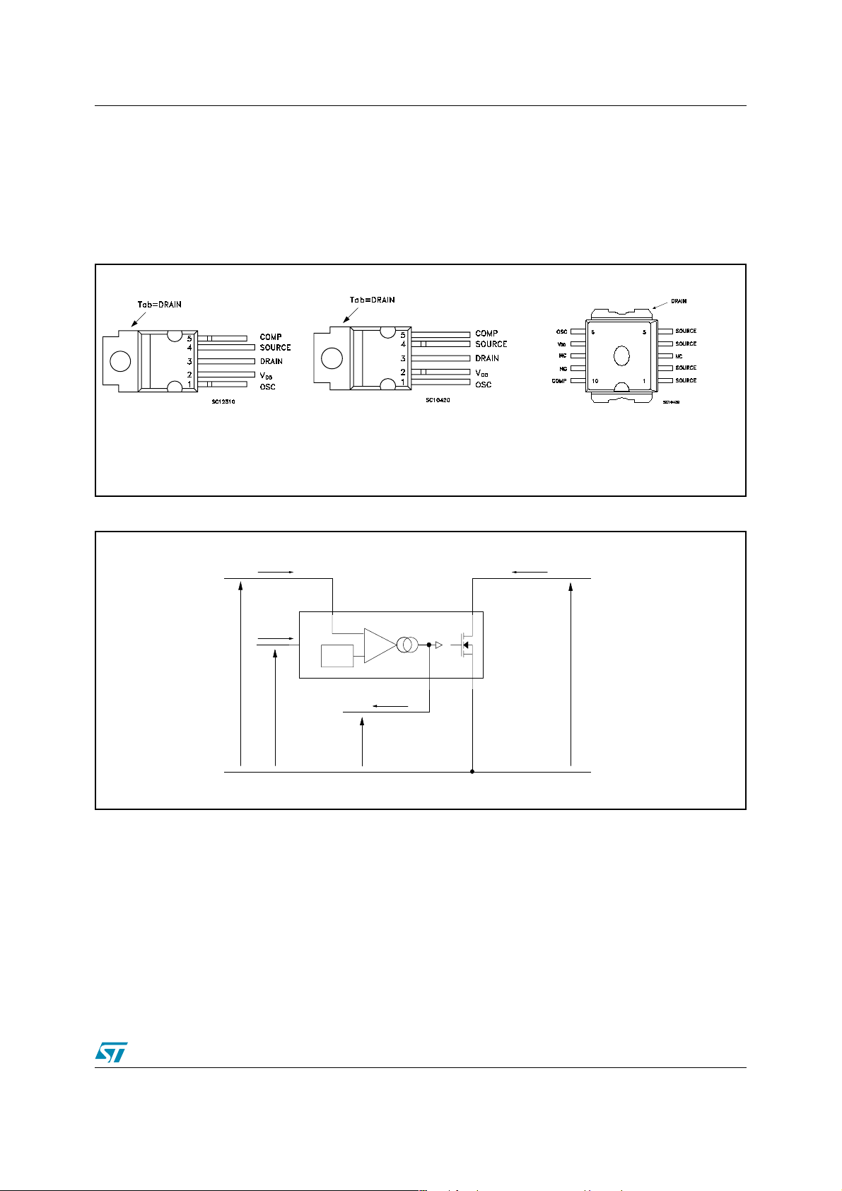
Figure 1. Connection Diagrams (T o p View)
to VDD, no significant frequency change occurs for VDD varying
t
PENTAWATT HV
PENTAWATT HV (022Y)
Figure 2. Current and Voltage Convention
IDD ID
IOSC
OSC
VDD
VOSC
13V
+
VCOMP
COMP SOURCE
ICOMP
PowerSO-10
DRAINVDD
VDS
TM
9/31
4 T ypical Circuit VIPer50A-E/ASP-E
4 Typical Circuit
Figure 3. Offline Power Supply With Auxiliary Supply Feedback
F1
BR1
TR1
D2
D1
C2
R1
C7
L2
+Vcc
C9
AC IN
TR2
C1
R9
D3
C4
C3
R7
R2
DRAINVDD
13V
+
C11
VIPer50
COMP SOURCE
C6
OSC
C5
R3
Figure 4. Offline Power Supply With Optocoupler Feedback
F1
BR1
TR1
D1
C2
C4
R1
D3
C3
R7
AC IN
TR2
C1
R9
GND
C10
FC00301
D2
C10
L2
+Vcc
C9C7
GND
R2
13V
+
C11
COMP SOURCE
C6
R3
OSC
C5
10/31
DRAINVDD
U1
VIPer100
R6
ISO1
R4
U2
C8
R5
FC00091
 Loading...