

VIPer22ADIP-E, VIPer22AS-E
Low power OFF-line SMPS primary switcher
Features
■ Fixed 60 kHz switching frequency
■ 9 V to 38 V wide range V
■ Current mode control
■ Auxiliary undervoltage lockout with hysteresis
■ High voltage start-up current source
■ Overtemperature, overcurrent and overvoltage
protection with auto-restart
Table 1. Typical power capability
Mains type SO-8 DIP-8
European (195 - 265 Vac) 12 W 20 W
US / wide range (85 - 265 Vac) 7 W 12 W
Description
voltage
DD
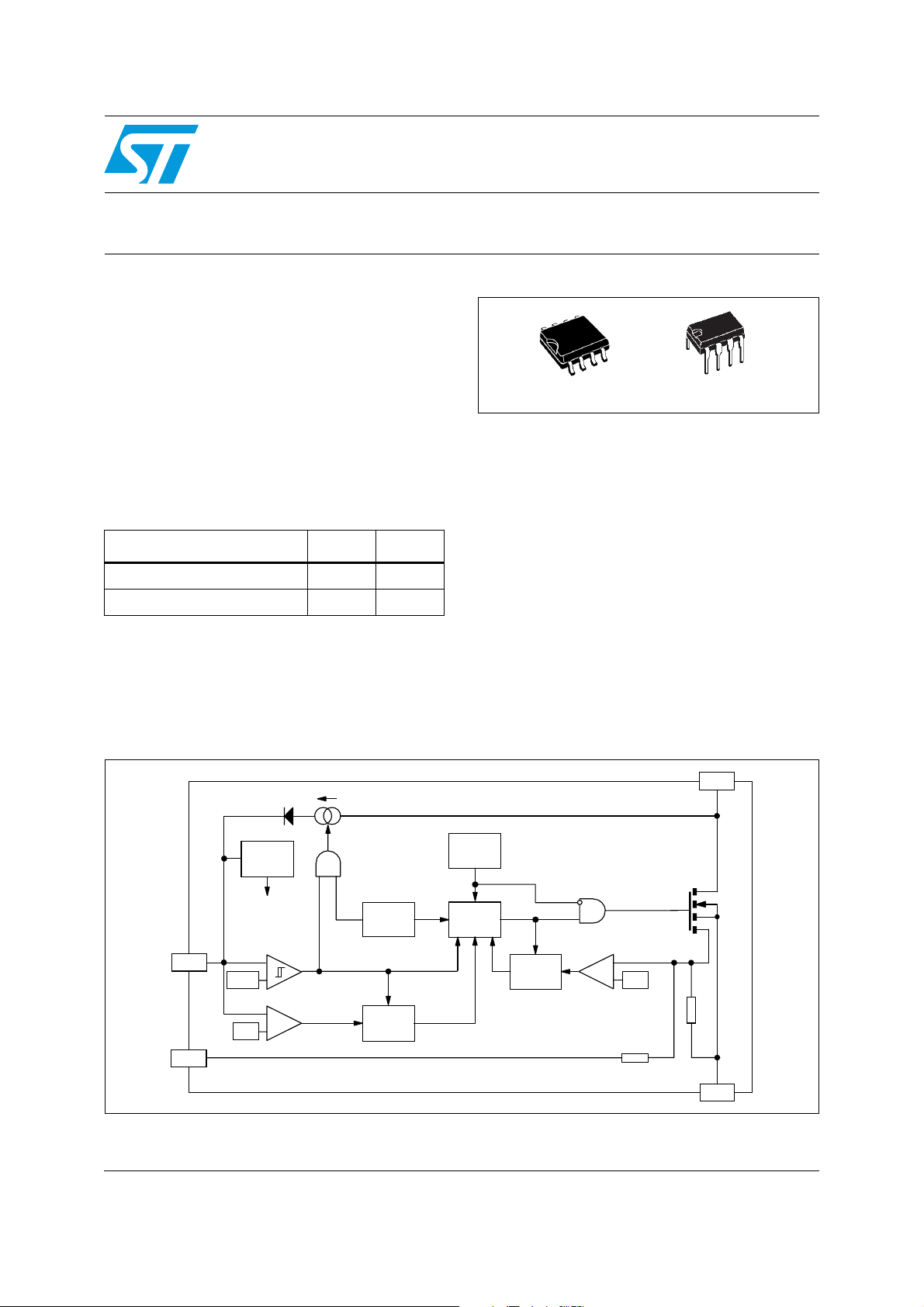
VIPer22A-E
DIP-8SO-8
Typical applications cover off line power supplies
for battery charger adapters, standby power
supplies for TV or monitors, auxiliary supplies for
motor control, etc. The internal control circuit
offers the following benefits:
Large input voltage range on the V
accommodates changes in auxiliary supply
voltage. This feature is well adapted to battery
charger adapter configurations.
Automatic burst mode in low load condition.
Overvoltage protection in HICCUP mode.
DD
pin
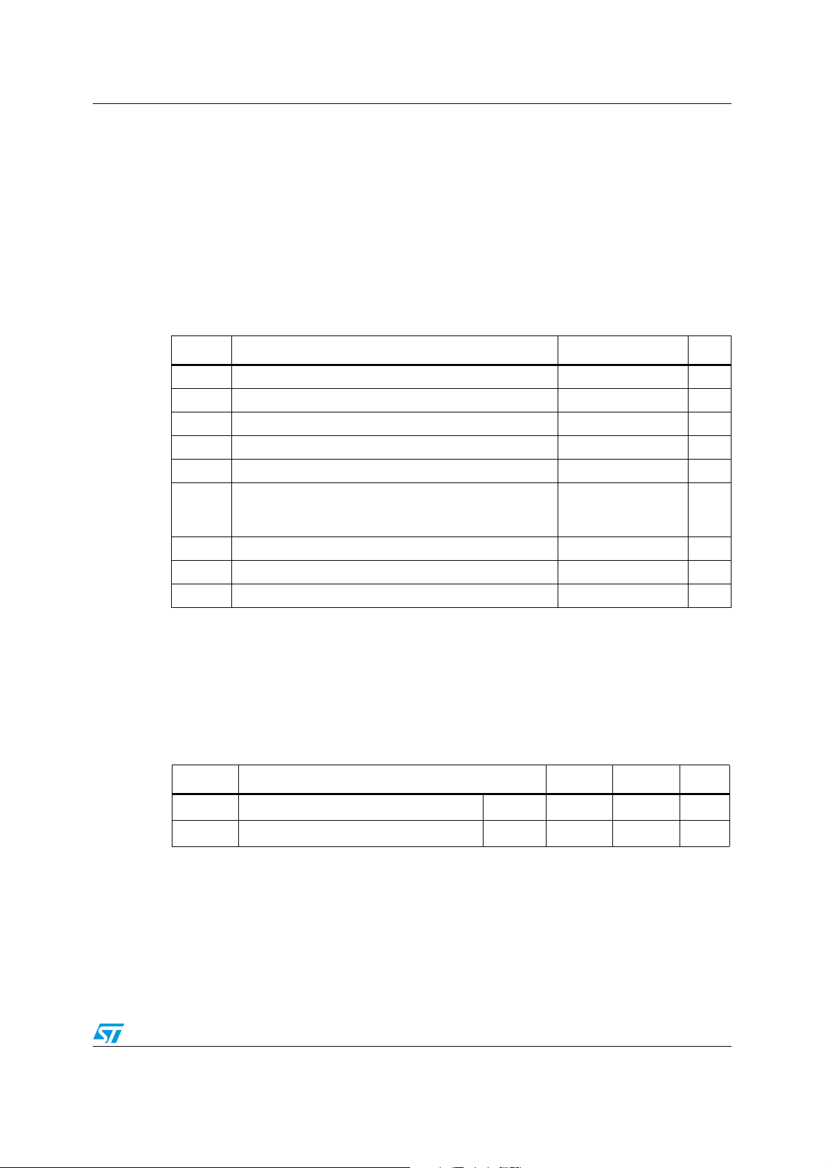
The VIPer22A-E combines a dedicated current
mode PWM controller with a high voltage power
MOSFET on the same silicon chip.
Figure 1. Block diagram
ON/OFF
REGULATOR
INTERNAL
VDD
FB
8/14.5V
42V
SUPPLY
_
+
+
_
OVERTEMP.
DETECTOR
R
FF
S
OVERVOLTAGE
Q
LATCH
60kHz
OSCILLATOR
S
FF
R1
R2
DRAIN
PWM
LATCH
R4QR3
BLANKING
+
_
0.23 V
230 Ω
1 kΩ
SOURCE
November 2010 Doc ID 12050 Rev 2 1/21
www.st.com
21

Contents VIPer22A-E, VIPer22ADIP-E, VIPer22AS-E
Contents
1 Electrical data . . . . . . . . . . . . . . . . . . . . . . . . . . . . . . . . . . . . . . . . . . . . . . 3
1.1 Maximum ratings . . . . . . . . . . . . . . . . . . . . . . . . . . . . . . . . . . . . . . . . . . . . 3
1.2 Thermal data . . . . . . . . . . . . . . . . . . . . . . . . . . . . . . . . . . . . . . . . . . . . . . . 3
2 Electrical characteristics . . . . . . . . . . . . . . . . . . . . . . . . . . . . . . . . . . . . . 4
3 Pin connections and function . . . . . . . . . . . . . . . . . . . . . . . . . . . . . . . . . 6
4 Operations . . . . . . . . . . . . . . . . . . . . . . . . . . . . . . . . . . . . . . . . . . . . . . . . . 7
4.1 Rectangular U-I output characteristics . . . . . . . . . . . . . . . . . . . . . . . . . . . . 7
4.2 Wide range of VDD voltage . . . . . . . . . . . . . . . . . . . . . . . . . . . . . . . . . . . . 8
4.3 Feedback pin principle of operation . . . . . . . . . . . . . . . . . . . . . . . . . . . . . . 8
4.4 Startup sequence . . . . . . . . . . . . . . . . . . . . . . . . . . . . . . . . . . . . . . . . . . . 11
4.5 Overvoltage threshold . . . . . . . . . . . . . . . . . . . . . . . . . . . . . . . . . . . . . . . 12
5 Operation pictures . . . . . . . . . . . . . . . . . . . . . . . . . . . . . . . . . . . . . . . . . 13
6 Package mechanical data . . . . . . . . . . . . . . . . . . . . . . . . . . . . . . . . . . . . 16
7 Order codes . . . . . . . . . . . . . . . . . . . . . . . . . . . . . . . . . . . . . . . . . . . . . . . 19
8 Revision history . . . . . . . . . . . . . . . . . . . . . . . . . . . . . . . . . . . . . . . . . . . 20
2/21 Doc ID 12050 Rev 2
VIPer22A-E, VIPer22ADIP-E, VIPer22AS-E Electrical data
1 Electrical data
1.1 Maximum ratings
Stressing the device above the rating listed in the “absolute maximum ratings” table may
cause permanent damage to the device. These are stress ratings only and operation of the
device at these or any other conditions above those indicated in the operating sections of
this specification is not implied. Exposure to absolute maximum rating conditions for
extended periods may affect device reliability.
Table 2. Absolute maximum rating
Symbol Parameter Value Unit
(2)
(1)
-0.3 ... 730 V
-0.3 ... 400 V
200
1.5
V
kV
V
Switching drain source voltage (TJ = 25 ... 125 °C)
DS(sw)
Start-up drain source voltage (TJ = 25 ... 125 °C)
V
DS(st)
I
Continuous drain current Internally limited A
D
Supply voltage 0 ... 50 V
V
DD
I
Feedback current 3 mA
FB
Electrostatic discharge:
V
Machine model (R = 0 Ω; C = 200 pF)
ESD
Charged device model
Junction operating temperature Internally limited °C
T
J
Case operating temperature -40 to 150 °C
T
C
T
1. This parameter applies when the start-up current source is OFF. This is the case when the VDD voltage
has reached V
2. This parameter applies when the start up current source is on. This is the case when the VDD voltage has
not yet reached V
Storage temperature -55 to 150 °C
stg
and remains above V
DDon
or has fallen below V
DDon
DDoff
.
DDoff.
1.2 Thermal data
Table 3. Thermal data
Symbol Parameter SO-8 DIP-8 Unit
R
thJC
R
thJA
1. When mounted on a standard single-sided FR4 board with 200 mm2 of Cu (at least 35 µm thick) connected
to all DRAIN pins.
Thermal resistance junction - case Max 25 15 °C/W
Thermal resistance junction - ambient
(1)
Max 55 45 °C/W
Doc ID 12050 Rev 2 3/21
Electrical characteristics VIPer22A-E, VIPer22ADIP-E, VIPer22AS-E
2 Electrical characteristics
TJ = 25 °C, V
= 18 V, unless otherwise specified
DD
Table 4. Power section
Symbol Parameter Test conditions Min Typ Max Unit
BV
Drain-source voltage ID = 1 mA; V
DSS
I
DSS
r
DS(on)
OFF state drain
current
Static drain-source
ON state resistance
t
Fall time
f
tr Rise time
Drain capacitance V
C
OSS
1. On clamped inductive load
V
= 500 V; V
DS
TJ = 125 °C
= 0.4 A
I
D
ID = 0.4 A; TJ = 100 °C
ID = 0.2 A; V
(See Figure 9 on page 13)
I
= 0.4 A; V
D
(See Figure 9 on page 13)
= 25 V 40 pF
DS
= 2 V 730 V
FB
= 2 V;
FB
0.1 mA
15 17
31
= 300 V
IN
= 300 V
IN
(1)
100 ns
(1)
50 ns
Ω
Table 5. Supply section
Symbol Parameter Test conditions Min Typ Max Unit
≤ 400 V;
DS
DDon
HYST
-1 mA
(1)
0 mA
4.5 mA
I
DDch
I
DDoff
I
DD0
I
DD1
Start-up charging
current
Start-up charging
current in thermal
shutdown
Operating supply
current not switching
Operating supply
current switching
100 V ≤ V
= 0 V ...V
V
DD
(See Figure 10 on page 13)
= 5 V; VDS = 100 V
V
DD
TJ > TSD - T
= 2 mA 3 5 mA
I
FB
I
= 0.5 mA; ID = 50 mA
FB
D
Restart duty-cycle (See Figure 11 on page 13) 16 %
RST
undervoltage
V
V
DDoff
V
DDon
V
DDhyst
V
DDovp
1. These test conditions obtained with a resistive load are leading to the maximum conduction time of the
device.
DD
shutdown threshold
start-up
V
DD
threshold
V
threshold
DD
hysteresis
overvoltage
V
DD
threshold
(See Figure 10,
Figure 11 on page 13)
(See Figure 10,
Figure 11 on page 13))
(See Figure 10 on page 13) 5.8 6.5 7.2 V
4/21 Doc ID 12050 Rev 2
7 8 9 V
13 14.5 16 V
38 42 46 V

VIPer22A-E, VIPer22ADIP-E, VIPer22AS-E Electrical characteristics
Table 6. Oscillation section
Symbol Parameter Test conditions Min Typ Max Unit
F
Oscillator frequency
OSC
total variation
= V
V
DD
TJ = 0 ... 100 °C
DDoff
... 35 V;
54 60 66 kHz
Table 7. PWM comparator section
Symbol Parameter Test conditions Min Typ Max Unit
G
I
Dlim
I
FBsd
RFB
t
ID
d
I
to ID current gain (See Figure 12 on page 14) 560
FB
Peak current
limitation
I
shutdown current (See Figure 12 on page 14) 0.9 mA
FB
FB pin input
impedance
Current sense delay
to turn-OFF
= 0 V
V
FB
(See Figure 12 on page 14)
= 0 mA
I
D
(See Figure 12 on page 14)
I
= 0.4 A 200 ns
D
0.56 0.7 0.84 A
1.2 kΩ
tb Blanking time 500 ns
t
ONmin
Minimum turn-ON
time
700 ns
Table 8. Overtemperature section
Symbol Parameter Test conditions Min Typ Max Unit
TSD
T
HYST
Table 9. Typical power capability
Thermal shutdown
temperature
Thermal shutdown
hysteresis
(See Figure 13 on page 14) 140 170 °C
(See Figure 13 on page 14) 40 °C
(1)
Mains type SO-8 DIP-8
European (195 - 265 Vac) 12 W 20 W
US / Wide range (85 - 265 Vac) 7 W 12 W
1. Above power capabilities are given under adequate thermal conditions
Doc ID 12050 Rev 2 5/21
Pin connections and function VIPer22A-E, VIPer22ADIP-E, VIPer22AS-E
3 Pin connections and function
Figure 2. Pin connection
SOURCE
SOURCE
FB
VDD
1
2
3
4
8
7
6
5
DRAIN
DRAIN
DRAIN
DRAIN
SO-8 DIP-8
Figure 3. Current and voltage conventions
I
DD
I
FB
V
DD
V
FB
VDD DRAIN
FB
CONTROL
VIPer22A
SOURCE
SOURCE
SOURCE
FB
VDD
1
2
3
4
I
D
V
D
8
DRAIN
7
DRAIN
6
DRAIN
5
DRAIN
Table 10. Pin function
Pin Name Pin function
Power supply of the control circuits. Also provides a charging current during start up
thanks to a high voltage current source connected to the drain. For this purpose, an
hysteresis comparator monitors the V
V
DD
SOURCE Power MOSFET source and circuit ground reference.
DRAIN
FB
6/21 Doc ID 12050 Rev 2
: Voltage value (typically 14.5 V) at which the device starts switching and turns
- V
DDon
off the start up current source.
: Voltage value (typically 8 V) at which the device stops switching and turns on
- V
DDoff
the start up current source.
Power MOSFET drain. Also used by the internal high voltage current source during
start up phase for charging the external VDD capacitor.
Feedback input. The useful voltage range extends from 0 V to 1 V, and defines the
peak drain MOSFET current. The current limitation, which corresponds to the
maximum drain current, is obtained for a FB pin shorted to the SOURCE pin.
voltage and provides two thresholds:
DD
VIPer22A-E, VIPer22ADIP-E, VIPer22AS-E Operations
4 Operations
4.1 Rectangular U-I output characteristics
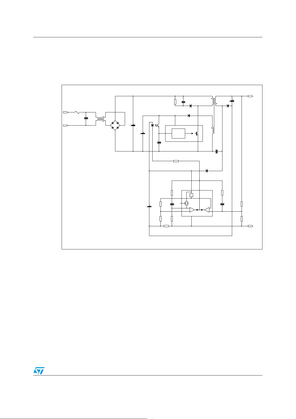
Figure 4. Rectangular U-I output characteristics for battery charger
AC IN
R1
C2
D1
F1
T2
C3
D4
C4
-+
ISO1
U1
C6
FB
VIPerX2A
R7R5R8
R10
C5
C10
D3
VDD DRAIN
CONTROL
SOURCE
R2
U2
R3
C8
TSM101
Vcc
Vref
-
+
GND
T1
C7
D5
+
-
C1
D2
R4
C9
DCOUT
R6
R9
GND
A complete regulation scheme can achieve combined and accurate output characteristics.
Figure 4. presents a secondary feedback through an optocoupler driven by a TSM101. This
device offers two operational amplifiers and a voltage reference, thus allowing the regulation
of both output voltage and current. An integrated OR function performs the combination of
the two resulting error signals, leading to a dual voltage and current limitation, known as a
rectangular output characteristic. This type of power supply is especially useful for battery
chargers where the output is mainly used in current mode, in order to deliver a defined
charging rate. The accurate voltage regulation is also convenient for Li-ion batteries which
require both modes of operation.
Doc ID 12050 Rev 2 7/21
 Loading...