

现货库存、技术资料、百科信息、热点资讯,精彩尽在鼎好!
Low Power OFF-Line SMPS Primary Switcher
Features
■ Fixed 60kHZ Switching Frequency
■ 9V to 38V Wide Range V
■ Current Mode Control
■ Auxiliary Undervoltage Lockout with Hysteresis
■ High Voltage Start-up Current Source
■ Overtemperature, Overcurrent and
Overvoltage Protection with Auto-Restart
Typical Power Capability
Voltage
DD
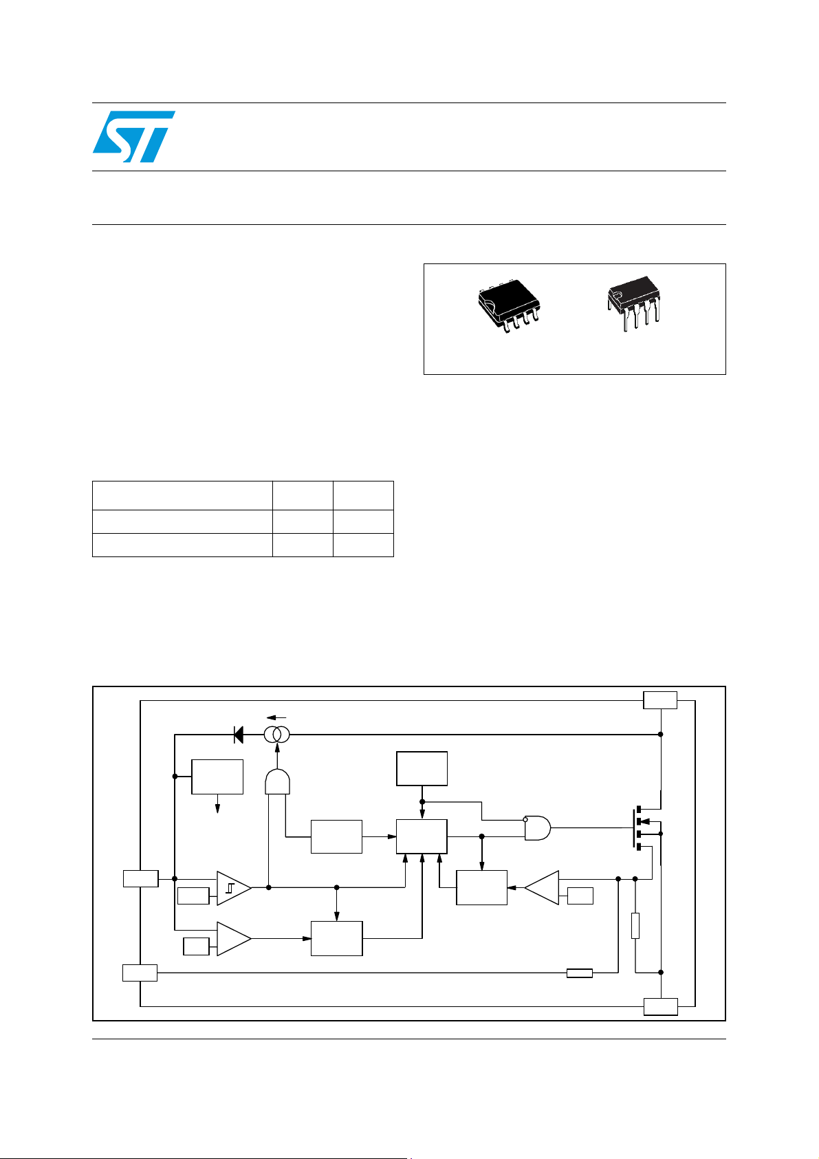
VIPer22ADIP - E
VIPer22AS - E
DIP-8SO-8
Description
The VIPer22A-E combines a dedicated current
mode PWM controller with a high voltage Power
MOSFET on the same silicon chip.
Mains type SO-8 DIP-8
European (195 - 265 Vac) 12W 20W
US / Wide range (85 - 265 V ac ) 7W 12W
Block diagram
ON/OFF
REGULATOR
INTERNAL
VDD
FB
8/14.5V
42V
SUPPLY
_
+
+
_
OVERTEMP.
DETECTOR
R
FF
S
OVERVOLTAGE
Q
LATCH
Typical applications cover off line power supplies
for battery charger adapters, standby power
supplies for TV or monitors, auxiliary supplies for
motor control, etc. The internal control circuit
offers the following benefits:
– L arge input voltage range on the V
accommodates changes in auxiliary supply
voltage. This feature is well adapted to
battery charger adapter configurations.
– Automatic burst mode in low load condition.
– Overvoltage protection in HICCUP mode.
DRAIN
60kHz
OSCILLATOR
PWM
S
LATCH
FF
R1
R4QR3
R2
BLANKING
+
_
0.23 V
Ω
230
Ω
1 k
DD
pin
SOURCE
February 2006 Rev1 1/20
www.st.com
20

Contents VIPer22ADIP/ VIPer22AS - E
Contents
1 Electrical Data . . . . . . . . . . . . . . . . . . . . . . . . . . . . . . . . . . . . . . . . . . . . . . 3
1.1 Ma ximum Ratings . . . . . . . . . . . . . . . . . . . . . . . . . . . . . . . . . . . . . . . . . . . . 3
1.2 Th ermal Data . . . . . . . . . . . . . . . . . . . . . . . . . . . . . . . . . . . . . . . . . . . . . . . 3
2 Electrical Characteristics . . . . . . . . . . . . . . . . . . . . . . . . . . . . . . . . . . . . . 4
3 Pin Connections and Function . . . . . . . . . . . . . . . . . . . . . . . . . . . . . . . . 6
4 Operations . . . . . . . . . . . . . . . . . . . . . . . . . . . . . . . . . . . . . . . . . . . . . . . . . 7
4.1 Re ctangular U-I Output Characteristics . . . . . . . . . . . . . . . . . . . . . . . . . . . 7
4.2 Wide Range of VDD Voltage . . . . . . . . . . . . . . . . . . . . . . . . . . . . . . . . . . . 7
4.3 Fe edback Pin Principle of Operation . . . . . . . . . . . . . . . . . . . . . . . . . . . . . 8
4.4 Startup sequence . . . . . . . . . . . . . . . . . . . . . . . . . . . . . . . . . . . . . . . . . . . 10
4.5 O vervoltage threshold . . . . . . . . . . . . . . . . . . . . . . . . . . . . . . . . . . . . . . . .11
5 Operation pictures . . . . . . . . . . . . . . . . . . . . . . . . . . . . . . . . . . . . . . . . . 12
6 Mechanical Data . . . . . . . . . . . . . . . . . . . . . . . . . . . . . . . . . . . . . . . . . . . 15
7 Order codes . . . . . . . . . . . . . . . . . . . . . . . . . . . . . . . . . . . . . . . . . . . . . . . 18
8 Revision history . . . . . . . . . . . . . . . . . . . . . . . . . . . . . . . . . . . . . . . . . . . 19
2/20 Rev1
VIPer22ADIP/ VIPer22AS - E Electrical Data
1 Electrical Data
1.1 Maximum Ratings
Stressing the device above the rating listed in the “Absolute Maximum Ratings” table may
cause permanent damage to the device. These are stress ratings only and operation of the
device at these or any other conditions above those indicated in the Operating sections of
this specification is not implied. Exposure to Absolute Maximum Rating conditions for
extended periods may affect device reliability. Refer also to the STMicroelectronics SURE
Program and other relevant quality documents.
Table 1. Absolute Maximum Rating
Symbol Parameter Value Unit
(2)
(1)
-0.3 ... 730 V
-0.3 ... 400 V
200
1.5
V
kV
V
Switching drain source voltage (TJ = 25 ... 125°C)
DS(sw)
V
St art-up drain source voltage (TJ = 25 ... 125°C)
DS(st)
I
Continuous drain current Internally limited A
D
V
Supply voltag e 0 ... 50 V
DD
I
Feedback current 3 mA
FB
Electrostatic discharge:
V
Machine model (R = 0Ω; C = 200pF)
ESD
Charged device model
T
Junction operating temperat ure Internally limited °C
J
T
Case operating temperature -40 to 150 °C
C
T
1. This parameter applies when the start-up current source is OFF. This is the case when the VDD voltage
has reached V
2. This parameter applies when the start up current source is on. This is the case when the VDD voltage has
not yet reached V
Storage Temperature -55 to 150 °C
stg
DDon
DDon
1.2 Thermal Data
Table 2. Thermal Data
Symbol Parameter SO-8 DIP-8 Unit
R
thJC
R
thJA
1. When mounted on a standard single-sided FR4 board with 200 mm2 of Cu (at least 35 µm thick)
connec te d to all DRAIN pin s.
Thermal Resist ance Junction - Case Max 25 15 °C/W
Thermal Resist ance Junction - Ambient
and remai ns abo v e V
or has fallen bel ow V
DDoff
.
DDoff.
(1)
Max 55 45 °C/W
Rev1 3/20
Electrical Characteristics VIPer22ADIP/ VIPer22AS - E
2 Electrical Characteristics
TJ = 25°C, V
= 18V, unless otherwise specified
DD
Table 3. Power section
Symbol Parameter Test conditions Min. Typ. Max. Unit
BV
Drain-source voltage ID = 1mA; V
DSS
I
DSS
r
DS(on)
C
1. On cl amped inductive load
OFF State drain
current
Static drain-source
ON state resistance
t
Fall time
f
Rise time
t
r
Drain capacitance V
OSS
V
= 500V; V
DS
T
= 125°C
J
= 0.4A
I
D
I
= 0.4A; TJ = 100°C
D
= 0.2A; V
I
D
(See Figure 8 on page12)
= 0.4A; V
I
D
(See Figure 8 on page12)
= 25V 40 pF
DS
= 2V 730 V
FB
= 2V;
FB
0.1 mA
15 17
31
= 300V
IN
= 300V
IN
(1)
100 ns
(1)
50 ns
Ω
Table 4. Supply section
Symbol Parameter Test conditions Min. Typ. Max. Unit
I
DDch
St art-up charging
current
V
= 100V; V
DS
= 0V ...V
DD
(See Figure 9 on page 12)
DDon
-1 mA
St art-up charging
I
DDoff
current in thermal
shutdown
Operating supply
I
DD0
I
DD1
D
V
DDoff
V
DDon
V
DDhyst
V
DDovp
1. These test conditions obtained with a resistive load are leading to the maximum conduction time of the
device.
current not switching
Operating supply
current switching
Restart duty-cycle (See Figure 10 on page 12) 16 %
RST
Undervoltage
V
DD
shutdown threshold
Start-up
V
DD
threshold
Threshold
V
DD
hysteresis
Overvoltage
V
DD
threshold
= 5V; VDS = 100V
V
DD
T
> TSD - T
J
I
= 2mA 3 5 mA
FB
I
= 0.5mA; ID = 50mA
FB
HYST
(1)
(See Figure 9,
Figure 10 on page 12)
(See Figure 9,
Figure 10 on page 12))
0 mA
4.5 mA
7 8 9 V
13 14.5 16 V
(See Figure 9 on page 12) 5.8 6.5 7.2 V
38 42 46 V
4/20 Rev1

VIPer22ADIP/ VIPer22AS - E E lectrica l Characteristics
Tabl e 5. Oscillation section
Symbol Parameter Test conditions Min. Typ. Max. Unit
F
Oscillato r fr equency
OSC
total var iat ion
V
= V
DD
T
DDoff
= 0 ... 100°C
J
... 35V;
54 60 66 kHz
Table 6. PWM Comparator section
Symbol Parameter Test Conditions Min. Typ. Max. Unit
G
I
ID
I
Dlim
I
FBsd
R
FB
t
d
t
Blanking time 500 ns
b
t
ONmin
to ID current gai n (See Figure 11 on page 13) 560
FB
Peak current
limitation
I
Shutdown current (See Figure 11 on page 13) 0.9 mA
FB
FB Pin input
impedance
Current sense del ay
to turn-OFF
Minimum Turn-ON
time
= 0V
V
FB
(See Figure 11 on page 13)
= 0mA
I
D
(See Figure 11 on page 13)
I
= 0.4A 200 ns
D
0.56 0.7 0.84 A
1.2 kΩ
700 ns
Tabl e 7. Overtemperature section
Symbol Parameter Test Conditions Min. Typ. Max. Unit
Thermal shutdown
T
SD
temperature
T
HYST
Thermal shutdown
hysteresis
Tabl e 8. Typical Power Capability
(See Figure 12 on page 13) 140 170 °C
(See Figure 12 on page 13) 40 °C
(1)
Mains type SO-8 DIP-8
European (195 - 265 Vac) 12W 20W
US / Wide range (85 - 265 Vac) 7W 12W
1. Above power capabilities are given under ad equate thermal condit ions
Rev1 5/20
Pin Connectio ns and Function VIPer22ADIP/ VIPer22AS - E
3 Pin Connections and Function
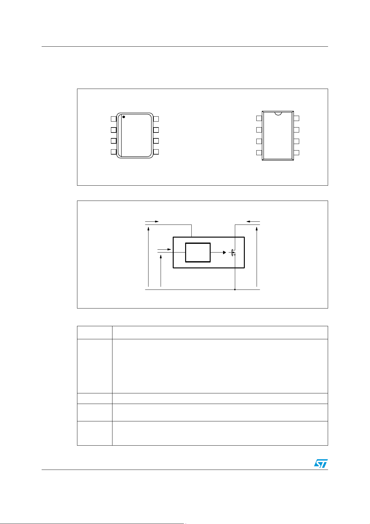
Figure 1. Pin connection
SOURCE
SOURCE
FB
VDD
1
2
3
4
8
7
6
5
DRAIN
DRAIN
DRAIN
DRAIN
SO-8 DIP-8
Figure 2. Current and voltage conventions
I
DD
I
FB
V
DD
V
FB
VDD DRAIN
FB
CONTROL
VIPer22A
SOURCE
SOURCE
SOURCE
FB
VDD
1
2
3
4
I
D
V
D
8
DRAIN
7
DRAIN
6
DRAIN
5
DRAIN
Table 9. P in func tion
Pin Name Pin Function
Power supply of the control circuits. Also provides a charging current during start up
thanks to a high voltage current source connected to the drain. For this purpose, an
hysteresis comparator monitors the V
V
DD
SOURCE Power MOSFET source and circuit gr ound reference.
DRAIN
FB
6/20 Rev1
: V oltage value (typically 14.5V) at which the devi ce starts swit ching and turns
- V
DDon
off the start up current source.
- V
: Voltage value (typically 8V) at which the device stops switching and turns on
DDoff
the start up current source.
Power MOSFET drain. Also used by the internal high voltage current source during
start up phase for charging the external V
Feedback input. The useful volt age ran ge ex tends f rom 0V to 1V, and defines th e peak
drain MOSFET current. The current limitation, which corresponds to the maximum
drain current, is obtained for a FB pin shorted to the SOURCE pin.
voltage and provides two thresholds:
DD
capacitor.
DD
 Loading...