


Features
DIP-7
SSO10
6)0%2
$2!). #/-0
'.$ &",)-
6$$
!-V
$#INPUTVOLTAGE
$#OUTPUTVOLTAGE
■ 800 V avalanche rugged power section
■ PWM operation with frequency jittering for low
EMI
■ Operating frequency:
– 30 kHz for VIPER06Xx
– 60 kHz for VIPER06Lx
– 115 kHz for VIPER06Hx
■ No need for an auxiliary winding in low-power
applications
■ Standby power < 30 mW at 265 V
Limiting current with adjustable set point
■
■ On-board soft-start
■ Safe auto-restart after a fault condition
■ Hysteretic thermal shutdown
AC
VIPER06
Fixed-frequency VIPer™ plus family
Datasheet — production data
Figure 1. Typical application
Applications
■ Replacement of capacitive power supplies
■ Home appliances
■ Power metering
■ LED drivers
Description
The VIPER06 is an offline converter with an 800 V
avalanche rugged power section, a PWM
controller, a user-defined overcurrent limit, openloop failure protection, hysteretic thermal
protection, soft startup and safe auto-restart after
any fault condition. The device is able to power
itself directly from the rectified mains, eliminating
the need for an auxiliary bias winding. Advanced
frequency jittering reduces EMI filter cost. Burst
mode operation and the device’s very low power
consumption both help to meet the standards set
by energy-saving regulations.
March 2012 Doc ID 022794 Rev 1 1/28
This is information on a product in full production.
www.st.com
28

Contents VIPER06
Contents
1 Block diagram . . . . . . . . . . . . . . . . . . . . . . . . . . . . . . . . . . . . . . . . . . . . . . 4
2 Typical power . . . . . . . . . . . . . . . . . . . . . . . . . . . . . . . . . . . . . . . . . . . . . . . 4
3 Pin settings . . . . . . . . . . . . . . . . . . . . . . . . . . . . . . . . . . . . . . . . . . . . . . . . 5
4 Electrical data . . . . . . . . . . . . . . . . . . . . . . . . . . . . . . . . . . . . . . . . . . . . . . 6
4.1 Maximum ratings . . . . . . . . . . . . . . . . . . . . . . . . . . . . . . . . . . . . . . . . . . . . 6
4.2 Thermal data . . . . . . . . . . . . . . . . . . . . . . . . . . . . . . . . . . . . . . . . . . . . . . . 6
4.3 Electrical characteristics . . . . . . . . . . . . . . . . . . . . . . . . . . . . . . . . . . . . . . . 7
5 Typical electrical characteristics . . . . . . . . . . . . . . . . . . . . . . . . . . . . . . 10
6 Typical circuit . . . . . . . . . . . . . . . . . . . . . . . . . . . . . . . . . . . . . . . . . . . . . 13
7 Power section . . . . . . . . . . . . . . . . . . . . . . . . . . . . . . . . . . . . . . . . . . . . . 15
8 High voltage current generator . . . . . . . . . . . . . . . . . . . . . . . . . . . . . . . 15
9 Oscillator . . . . . . . . . . . . . . . . . . . . . . . . . . . . . . . . . . . . . . . . . . . . . . . . . 16
10 Soft startup . . . . . . . . . . . . . . . . . . . . . . . . . . . . . . . . . . . . . . . . . . . . . . . 16
11 Adjustable current limit set point . . . . . . . . . . . . . . . . . . . . . . . . . . . . . 16
12 FB pin and COMP pin . . . . . . . . . . . . . . . . . . . . . . . . . . . . . . . . . . . . . . . 17
13 Burst mode . . . . . . . . . . . . . . . . . . . . . . . . . . . . . . . . . . . . . . . . . . . . . . . 18
14 Automatic auto-restart after overload or short-circuit . . . . . . . . . . . . 19
15 Open-loop failure protection . . . . . . . . . . . . . . . . . . . . . . . . . . . . . . . . . 20
16 Package mechanical data . . . . . . . . . . . . . . . . . . . . . . . . . . . . . . . . . . . . 22
2/28 Doc ID 022794 Rev 1

VIPER06 Contents
17 Order codes . . . . . . . . . . . . . . . . . . . . . . . . . . . . . . . . . . . . . . . . . . . . . . . 26
18 Revision history . . . . . . . . . . . . . . . . . . . . . . . . . . . . . . . . . . . . . . . . . . . 27
Doc ID 022794 Rev 1 3/28

Block diagram VIPER06
OLP
LOGIC
+
-
E/A
VDD
GND
+
-
PWM
Oscillator
LEB
BURST-MODE
Logic
TURN-ON
LOGIC
SOFT START
UVLO
BURST
OTP
LIM
V
COMPL
HV_ON
SUPPLY
&
UVLO
I
DDch
V
REF_FB
THERMAL
SHUTDOWN
DRAIN
+
-
OCP
I
DLIM
set-up
S
R
Q
Burst
R
SENSE
OTP
Internal Supply BUS &
REFERENCE VOLTAGES
COMP
FB
1 Block diagram
Figure 2. Block diagram
2 Typical power
Table 1. Typical power
230 V
Part number
Adapter
VIPER06 6 W 8 W 4 W 5 W
1. Typical continuous power in non-ventilated enclosed adapter measured at 50 ° C ambient.
2. Maximum practical continuous power in an open-frame design at 50 ° C ambient, with adequate heat
sinking.
4/28 Doc ID 022794 Rev 1
(1)
AC
Open frame
(2)
Adapter
85-265 V
(1)
AC
Open frame
(2)

VIPER06 Pin settings
DRAIN
DRAIN
AM11339v1
DRAIN
DRAIN
DRAIN
DRAIN
DRAIN
GND
VDD
FB
COMP
LIM
3 Pin settings
Figure 3. Connection diagram (top view)
Note: The copper area for heat dissipation has to be designed under the DRAIN pins.
Table 2. Pin description
Pin
Name Function
DIP-7 SSO10
11GND
22VDD
33LIM
44FB
55COMP
7, 8 6-10 DRAIN
Connected to the source of the internal power MOSFET and controller
ground reference.
Supply voltage of the control section. This pin provides the charging
current of the external capacitor.
This pin allows setting the drain current limitation. The limit can be
reduced by connecting an external resistor between this pin and GND.
Pin left open if default drain current limitation is used.
Inverting input of the internal transconductance error amplifier.
Connecting the converter output to this pin through a single resistor
results in an output voltage equal to the error amplifier reference
voltage (see V
in Table 6). An external resistor divider is
FB_REF
required for higher output voltages.
Output of the internal transconductance error amplifier. The
compensation network has to be placed between this pin and GND to
achieve stability and good dynamic performance of the voltage control
loop. The pin is used also to directly control the PWM with an
optocoupler. The linear voltage range extends from V
V
COMPH
(Ta bl e 6 ).
COMPL
to
High-voltage drain pins. The built-in high-voltage switched startup bias
current is drawn from these pins too.
Pins connected to the metal frame to facilitate heat dissipation.
Doc ID 022794 Rev 1 5/28

Electrical data VIPER06
4 Electrical data
4.1 Maximum ratings
Table 3. Absolute maximum ratings
Symbol
V
DRAIN
E
AV
I
AR
I
DRAIN
V
COMP
V
FB
V
LIM
V
DD
I
DD
P
TOT
T
J
T
STG
Pin
(DIP-7)
Parameter
Value
Min Max
7, 8 Drain-to-source (ground) voltage 800 V
7, 8 Repetitive avalanche energy (limited by TJ = 150 °C) 2 mJ
7, 8 Repetitive avalanche current (limited by TJ = 150 °C) 1 A
7, 8 Pulse drain current (limited by TJ = 150 °C) 2.5 A
5 Input pin voltage -0.3 3.5 V
4 Input pin voltage -0.3 4.8 V
3 Input pin voltage -0.3 2.4 V
2 Supply voltage -0.3
Self-
limited
2 Input current 20 mA
Power dissipation at TA < 40 °C (DIP-7) 1 W
Power dissipation at T
< 50 °C (SSO10) 1 W
A
Operating junction temperature range -40 150 °C
Storage temperature -55 150 °C
Unit
V
4.2 Thermal data
Table 4. Thermal data
Symbol Parameter
R
R
R
1. When mounted on a standard single side FR4 board with 100 mm2 (0.155 sq in) of Cu (35 μm thick).
6/28 Doc ID 022794 Rev 1
Thermal resistance junction pin
thJP
(dissipated power = 1 W)
Thermal resistance junction ambient
thJA
(dissipated power = 1 W)
Thermal resistance junction ambient
thJA
(dissipated power = 1 W)
(1)
Max value
SSO10
Max value
DIP-7
35 40 ° C/W
100 110 ° C/W
80 90 ° C/W
Unit

VIPER06 Electrical data
4.3 Electrical characteristics
(TJ = -25 to 125 °C, VDD = 14 V
Table 5. Power section
Symbol Parameter Test condition Min Typ Max Unit
V
BVDSS
I
OFF
R
DS(on)
C
OSS
Table 6. Supply section
Symbol Parameter Test condition Min Typ Max Unit
Vol tag e
Breakdown voltage
OFF state drain current
Drain-source on-state resistance
Effective (energy related) output capacitance V
(a)
unless otherwise specified).
I
= 1 mA,
DRAIN
V
= GND, TJ = 25 °C
COMP
V
V
I
I
= max rating,
DRAIN
= GND
COMP
= 0.2 A, TJ = 25 °C 32 Ω
DRAIN
= 0.2 A, TJ = 125 °C 67 Ω
DRAIN
= 0 to 640 V 10 pF
DRAIN
800 V
60 μA
V
_START
DRAIN
I
DDch1
I
DDch2
V
DD
V
DDclampVDD
V
DDon
V
DDCSon
V
DDoff
Current
I
DD0
I
DD1
I
DDoff
I
DDol
Drain-source startup voltage 25 45 V
= 100 V to 640 V,
V
Startup charging current
Charging current during operation
DRAIN
= 4 V
V
DD
= 100 V to 640 V,
V
DRAIN
= 9 V falling edge
V
DD
-0.6 -1.8 mA
-7 -14 mA
Operating voltage range 11.5 23.5 V
clamp voltage IDD = 15 mA 23.5 V
VDD startup threshold 12 13 14 V
VDD on internal high-voltage current
generator threshold
9.5 10.5 11.5 V
VDD undervoltage shutdown threshold 7 8 9 V
Operating supply current, not switching F
Operating supply current, switching
Operating supply current with VDD < V
DDoffVDD
Open-loop failure current threshold
OSC
V
DRAIN
F
OSC
V
DRAIN
F
OSC
V
DRAIN
F
OSC
V
DD
V
COMP
= 0 kHz, V
= 120 V,
= 30 kHz
= 120 V,
= 60 kHz
= 120 V,
= 115 kHz
< V
DDoff
= V
DDclamp
= 3.3 V,
= GND 0.6 mA
COMP
4 mA
1.3 mA
1.45 mA
1.6 mA
0.35 mA
a. Adjust VDD above V
startup threshold before setting to 14 V.
DDon
Doc ID 022794 Rev 1 7/28

Electrical data VIPER06
Table 7. Controller section
Symbol Parameter Test condition Min Typ Max Unit
Error amplifier
V
REF_FB
I
FB_PULL UP
G
M
FB reference voltage 3.2 3.3 3.4 V
Current pull-up -1 μA
Transconductance 2 mA/V
Current setting (LIM) pin
V
LIM_LOW
Low-level clamp voltage I
Compensation (COMP) pin
V
COMPH
V
COMPL
V
COMPL_HYS
H
COMP
R
COMP(DYN)
Upper saturation limit TJ = 25 °C 3 V
Burst mode threshold TJ = 25 °C 1 1.1 1.2 V
Burst mode hysteresis TJ = 25 °C 40 mV
ΔV
COMP
/ ΔI
DRAIN
Dynamic resistance V
Source / sink current V
I
COMP
Max source current V
Current limitation
I
Dlim
t
SS
T
ON_MIN
I
Dlim_bm
Drain current limitation
Soft-start time 8.5 ms
Minimum turn-on time 450 ns
Burst mode current limitation V
Overload
= -100 μA0.5V
LIM
49V/A
= GND 15 kΩ
FB
> 100 mV 150 μA
FB
COMP
= -10 μA, V
I
LIM
= 25 °C
T
J
COMP
= GND, V
= V
COMPL
= GND 220 μA
FB
= 3.3 V,
COMP
0.32 0.35 0.38 A
85 mA
t
OVL
t
RESTART
Overload time 50 ms
Restart time after fault 1 s
Oscillator section
VIPER06Xx 27 30 33 kHz
F
OSC
Switching frequency
VIPER06Lx 54 60 66 kHz
VIPER06Hx 103 115 127 kHz
= 30 kHz ±3 kHz
F
OSC
F
= 60 kHz ±4 kHz
OSC
F
= 115 kHz ±8 kHz
OSC
D
F
D
F
M
MAX
Modulation depth
Modulation frequency 230 Hz
Maximum duty cycle 70 80 %
8/28 Doc ID 022794 Rev 1

VIPER06 Electrical data
Table 7. Controller section (continued)
Symbol Parameter Test condition Min Typ Max Unit
Thermal shutdown
T
T
HYST
SD
Thermal shutdown temperature 150 160 °C
Thermal shutdown hysteresis 30 °C
Doc ID 022794 Rev 1 9/28

Typical electrical characteristics VIPER06
IDlim/ IDlim@2 5°C
0.94
0.96
0.98
1.00
1.02
1.04
-50 0 50 100 150
TJ [°C]
AM01144v1
AM01145v1
FOSC / FOSC@25°C
0.92
0.94
0.96
0.98
1.00
1.02
1.04
-50 0 50 100 150
TJ [°C]
AM01146v1
VDRAIN_START / VDRAIN_START@25°C
0.960
0.970
0.980
0.990
1.000
1.010
1.020
-50 0 50 100 150
TJ [°C]
AM01147v1
HCO M P / HC OM P@2 5°C
0.80
0.90
1.00
1.10
1.20
1.30
-50 0 50 100 150
TJ [°C]
AM01148v1
GM / GM@ 25°C
0.80
0.85
0.90
0.95
1.00
1.05
1.10
-50 0 50 100 150
TJ [°C]
AM01149v1
VR EF_F B / V REF_ FB@25°C
0.80
0.84
0.88
0.92
0.96
1.00
1.04
1.08
-50 0 50 100 150
TJ [°C]
5 Typical electrical characteristics
Figure 4. I
Figure 6. V
vs. TJ Figure 5. F
Dlim
DRAIN_START
vs. T
J
Figure 7. H
OSC
COMP
vs. T
vs. T
J
J
Figure 8. GM vs. T
10/28 Doc ID 022794 Rev 1
J
Figure 9. V
REF_FB
vs. T
J

VIPER06 Typical electrical characteristics
AM01150v1
ICOM P / ICOM P@25°C
0.80
0.84
0.88
0.92
0.96
1.00
1.04
1.08
-50 0 50 100 150
TJ [°C]
AM01151v1
IDD0 / IDD0 @25°C
0.80
0.84
0.88
0.92
0.96
1.00
1.04
1.08
-50 0 50 100 150
TJ [°C]
AM01152v1
IDD1 / IDD 1@25°C
0.60
0.65
0.70
0.75
0.80
0.85
0.90
0.95
1.00
1.05
1.10
-50 0 50 100 150
TJ [°C]
AM01153v1
IDlim / IDlim@100KOhm
0.00
0.10
0.20
0.30
0.40
0.50
0.60
0.70
0.80
0.90
1.00
1.10
020406080100
Rli m [ kO hm ]
Figure 10. I
COMP
vs. T
J
Figure 12. Operating supply current
(switching) vs. T
J
Figure 11. Operating supply current
Figure 13. I
(no switching) vs. T
Dlim
vs. R
LIM
J
Figure 14. Power MOSFET on-resistance
vs. T
J
Figure 15. Power MOSFET breakdown voltage
vs. T
J
Doc ID 022794 Rev 1 11/28
Typical electrical characteristics VIPER06
T
J
V
DD
I
DRAIN
V
DDon
time
V
DDCSon
V
DDoff
T
SD
time
time
T
SD -THYST
Shut down after over temperature
Normal operation Normal operation
Figure 16. Thermal shutdown
12/28 Doc ID 022794 Rev 1
VIPER06 Typical circuit
AM01197v1
VOUT
4
12
10
66
+
Cout
+
C2
Rcomp1
Ccl
CONTROL
FB
DRAIN
GND
VDD
COMP
LIM
VIPer16
AC IN
Rcl
D1
Rfb2
AC IN
Ccomp1
RLIM
Dout
Rfb1
Rin
Daux
-+
Din
1
4
3
2
(optional)
+
C3
C1
L1
Ccomp2
AM01195v1
-
AC IN
AC IN
VOUT
L1L1
C5C5
C3C3
C4C4
+C7+
C7
R3R3
R5R5
D3D3
CONTROL
FB
DRAIN
GND
VDD
COMP
LIM
VIPER06
CONTROL
FB
DRAIN
GND
VDD
COMP
LIM
VIPER06
+C2+
C2
C8C8R4R4
D1D1
+C1+
C1
R1R1
R6R6
T2T2
C6C6
IC2IC2
IC3IC3
D2D2
R2R2
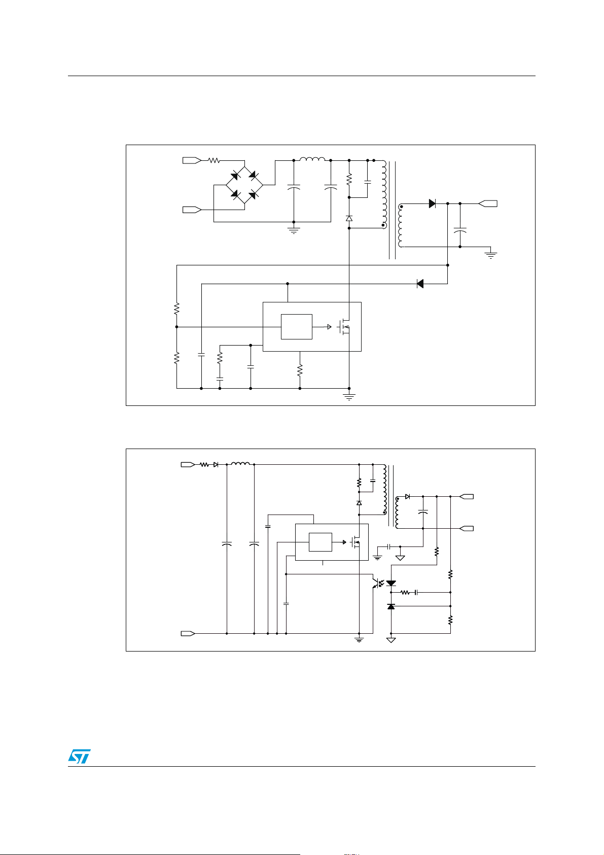
6 Typical circuit
Figure 17. Flyback converter (non-isolated output)
Figure 18. Flyback converter (isolated output)
Doc ID 022794 Rev 1 13/28

Typical circuit VIPER06
(optional)
Rfbl
L1
CONTROL
FB
DRAIN
GND
VDD
COMP
LIM
VIPer06
Rfbh
+
Cout
TRANSF
1
3
4
12
10
66
FUSE
Daux
+
CVDD
Rc
+
C1
D2
Rcl
Cfb
-+
D0
BRIDGE
1
4
3
2
D1
Cc
Cp RLIM
Ccl
+
C2
Raux
Vou t
AC IN
AC IN
.
AM01196v1
(optional)
CONTROL
FB
DRAIN
GND
VDD
COMP
LIM
VIPer06
Ccomp
Rfb2
Cout
C1
D2
Lout
C3
Rfb1
Rcomp
C4
L1
C2
RLIM
Cfb
Dout
AC IN
GND
Vout
AM01194v1
Figure 19. Flyback converter (isolated output without optocoupler)
Figure 20. Buck converter
14/28 Doc ID 022794 Rev 1
VIPER06 Power section
I
DD
V
DD
V
DRAIN
V
DDon
t
t
t
t
V
IN
V
DRAIN_START
t
t
Power-on
Power-off
Normal operat ion
regulation is lost here
VIN< V
DRAIN_START
HV startup is no more ac tivated
With internal self-supply
Without internal se lf-supply
V
DDCSon
V
DDoff
I
DDch1
I
DDch2
7 Power section
The power section is implemented with an N-channel power MOSFET with a breakdown
voltage of 800 V min. and a typical R
of 32 Ω. It includes a SenseFET structure to allow
DS(on)
virtually lossless current sensing and the thermal sensor.
The gate driver of the power MOSFET is designed to supply a controlled gate current during
both turn-ON and turn-OFF in order to minimize common-mode EMI. During UVLO
conditions, an internal pull-down circuit holds the gate low in order to ensure that the power
MOSFET cannot be turned ON accidentally.
8 High voltage current generator
The high-voltage current generator is supplied by the DRAIN pin. At the first startup of the
converter it is enabled when the voltage across the input bulk capacitor reaches the
V
DRAIN_START
voltage reaches the V
voltage current generator is turned OFF. The VIPER06 is powered by the energy stored in
the V
DD
In a steady-state condition, if the self-biasing function is used, the high-voltage current
generator is activated between V
I
, see Table 6 on page 7 to the VDD capacitor during the MOSFET off-time (see
DDch2
Figure 21).
threshold, sourcing a I
DDon
capacitor.
current (see Table 6 on page 7). As the VDD
DDch1
threshold, the power section starts switching and the high-
DDCSon
and V
(see Table 6 on page 7), delivering
DDon
The device can also be supplied through the auxiliary winding in which case the highvoltage current source is disabled during steady-state operation, provided that VDD is
above V
DDCSon
At converter power-down, the V
below the V
.
voltage drops and the converter activity stops as it falls
threshold (see Table 6 on page 7).
DDoff
DD
Figure 21. Power-on and power-off
Doc ID 022794 Rev 1 15/28

Oscillator VIPER06
9 Oscillator
The switching frequency is internally fixed at 30 kHz or 60 kHz or 115 kHz (respectively part
numbers VIPER06Xx, VIPER06Lx and VIPER06Hx).
The switching frequency is modulated by approximately ±3 kHz (30 kHz version) or ±4 kHz
(60 kHz version) or ±8 kHz (115 kHz version) at 230 Hz (typical) rate, so that the resulting
spread spectrum action distributes the energy of each harmonic of the switching frequency
over a number of sideband harmonics having the same energy on the whole, but smaller
amplitudes.
10 Soft startup
During the converter’s startup phase, the soft-start function progressively increases the
cycle-by-cycle drain current limit, up to the default value I
further limited and the output voltage is progressively increased, reducing the stress on the
secondary diode. The soft-start time is internally fixed to t
in Table 7 on page 8, and the function is activated for any attempt of converter startup and
after a fault event.
. In this way the drain current is
Dlim
, see typical value
SS
This function helps prevent saturation of the transformer during startup and short-circuit.
11 Adjustable current limit set point
The VIPER06 includes a current-mode PWM controller. The drain current is sensed cycleby-cycle through the integrated resistor R
inverting input of the PWM comparator, see Figure 2 on page 4. As soon as the sensed
voltage is equal to the voltage derived from the COMP pin, the power MOSFET is switched
OFF.
In parallel with the PWM operations, the comparator OCP, see Figure 2 on page 4, checks
the level of the drain current and switches OFF the power MOSFET in case the current is
higher than the threshold I
The level of the drain current limit I
, see Table 7 on page 8.
Dlim
can be reduced using a resistor R
Dlim
between the LIM and GND pins. Current is sunk from the LIM pin through the resistor R
and the setup of I
R
is shown in Figure 13 on page 11.
LIM
When the LIM pin is left open or if R
fixed to its default value, I
depends on the level of this current. The relation between I
Dlim
has a high value (i.e. > 80 kΩ), the current limit is
, as given in Table 7 on page 8.
Dlim
LIM
and the voltage is applied to the non-
SENSE
connected
LIM
Dlim
LIM
and
16/28 Doc ID 022794 Rev 1

VIPER06 FB pin and COMP pin
FB
COMP
Without Isolation:
switch open & E/A enabled
With Isolation:
switch closed & E/A disabled
No
Isolation
V
OUT
+
-
PWM stop
from R
SENSE
R
Isolation
R
L
nR
SW
V
REF
R
COMP
+
-
E/A
BUS
+
-
to PWM
V
COMPL
R
H
V
REF_FB
12 FB pin and COMP pin
The device can be used both in non-isolated and isolated topology. In non-isolated topology,
the feedback signal from the output voltage is applied directly to the FB pin as the inverting
input of the internal error amplifier having the reference voltage, V
page 8.
REF_FB,
see Ta b le 7 o n
The output of the error amplifier sources and sinks the current, I
, respectively to and
COMP
from the compensation network connected on the COMP pin. This signal is then compared
in the PWM comparator with the signal coming from the SenseFET in order to switch off the
power MOSFET on a cycle-by-cycle basis. See the Figure 2 on page 4 and the Figure 22.
When the power supply output voltage is equal to the error amplifier reference voltage,
V
REF_FB
, a single resistor has to be connected from the output to the FB pin. For higher
output voltages the external resistor divider is needed. If the voltage on the FB pin is
accidentally left floating, an internal pull-up protects the controller.
The output of the error amplifier is externally accessible through the COMP pin and it’s used
for the loop compensation, usually an RC network.
As shown in Figure 22, in case of an isolated power supply, the internal error amplifier has to
be disabled (FB pin shorted to GND). In this case an internal resistor is connected between
an internal reference voltage and the COMP pin, see Figure 22. The current loop has to be
closed on the COMP pin through the opto-transistor in parallel with the compensation
network. The V
dynamic range is between V
COMP
COMPL
and V
COMPH
shown in Figure 23 on
page 18.
When the voltage V
drops below the voltage threshold V
COMP
, the converter enters
COMPL
burst mode, see Section 13 on page 18.
When the voltage V
rises above the V
COMP
COMPH
threshold, the peak drain current, as well
as the deliverable output power, will reach its limit.
Figure 22. Feedback circuit
Doc ID 022794 Rev 1 17/28

Burst mode VIPER06
AM01095v1
V
COMPH
V
COMPL
I
Dlim_bm
I
Dlim
I
DRAIN
V
COMP
time
time
time
V
COMP
V
COMPL+VCOMPL_HYS
V
COMPL
I
DD1
I
DD0
I
DD
I
DRAIN
I
Dlim_bm
Burst Mode
Figure 23. COMP pin voltage versus I
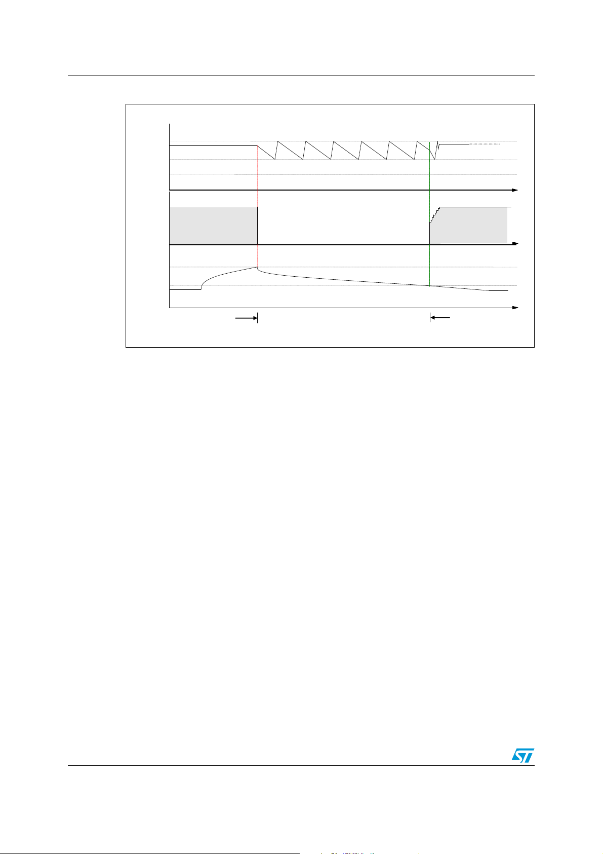
13 Burst mode
When the voltage V
the OFF state and the consumption is reduced to the I
page 7. In reaction to the loss of energy, the V
exceeds the threshold V
level of consumption equal to the I
“burst mode” and shown in Figure 24 on page 18, reduces the average frequency, which can
go down even to a few hundreds hertz, thus minimizing all frequency-related losses and
making it easier to comply with energy-saving regulations. During burst mode, the drain
current limit is reduced to the value I
audible noise issue.
DRAIN
drops below the threshold, V
COMP
+ V
COMPL
COMPL_HYS
current. This ON-OFF operation mode, referred to as
DD1
Dlim_bm
, the power MOSFET is kept in
COMPL
current, as reported on Ta ble 6 on
DD0
voltage increases and as soon as it
COMP
, the converter starts switching again with a
(given inTable 7 on page 8) in order to avoid the
Figure 24. Load-dependent operating modes: timing waveforms
18/28 Doc ID 022794 Rev 1

VIPER06 Automatic auto-restart after overload or short-circuit
time
time
V
DD
V
DDon
V
DDCSon
I
DRAIN
I
Dlim_bm
t
1
*
* The time t1 can be lower or equal to the time t
OVL
t
RESTART
t
SS
t
OVL
t
RESTART
t
SS
t
OVL
t
RESTART
t
SS
SHORT CIRCUIT
OCCURS HERE
SHORT CIRCUIT
REMOVED HERE
time
time
V
DD
V
DDon
V
DDCSon
I
DRAIN
I
Dlim_bm
t
1
*
* The time t1can be lower t han or equal to the time t
OVL
t
RESTART
t
SS
t
OVL
t
RESTART
t
SS
t
OVL
t
RESTART
t
SS
SHORT CIRCUIT
OCCURS HERE
SHORT CIRCUIT
REMOVED HERE
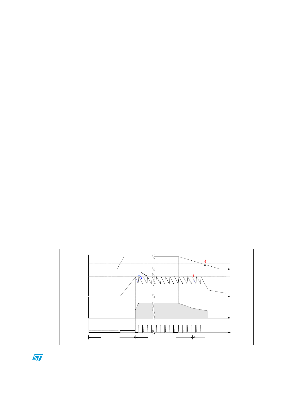
14 Automatic auto-restart after overload or short-circuit
The overload protection is implemented automatically using the integrated up-down counter.
Every cycle, it is incremented or decremented depending upon the current logic detection of
the limit condition or not. The limit condition is the peak drain current, I
on page 8 or the one set by the user through the R
resistor, shown in Figure 13 on
LIM
page 11. After the reset of the counter, if the peak drain current is continuously equal to the
level I
, the counter will be incremented until the fixed time, t
Dlim
, at which point the power
OVL
MOSFET switch ON will be disabled. It will be activated again through the soft-start after the
t
RESTART
time (see Figure 25 and Figure 26 on page 19) and the time values mentioned in
Table 7 on page 8.
For overload or short-circuit events, the power MOSFET switching will be stopped after a
period of time dependent upon the counter with a maximum equal to t
sequence continues until the overload condition is removed, see Figure 25 and Figure 26.
This protection ensures a low repetition rate of restart attempts of the converter, so that it
works safely with extremely low power throughput and avoids overheating the IC in case of
repeated overload events. If the overload is removed before the protection tripping, the
counter will be decremented cycle-by-cycle down to zero and the IC will not be stopped.
Figure 25. Timing diagram: OLP sequence (IC externally biased)
given in Ta bl e 7
Dlim ,
. The protection
OVL
Figure 26. Timing diagram: OLP sequence (IC internally biased)
Doc ID 022794 Rev 1 19/28

Open-loop failure protection VIPER06
V
COMPL
D
AUX
nR
FB
VDD
V
AUX
COMP
+
-
to PWM
R
L
+
-
E/A
R
H
R
R
AUX
C
VDD
V
OUT
R
S
V
REF_FB
from R
SENSE
BUS
+
-
PWM stop
C
S
C
P
15 Open-loop failure protection
If the power supply has been designed using flyback topology and the VIPER06 is supplied
by an auxiliary winding, as shown in Figure 27 and Figure 28 on page 21, the converter is
protected against feedback loop failure or accidental disconnections of the winding.
The following description is applicable for the schematics of Figure 27 and Figure 28 on
page 21, respectively the non-isolated flyback and the isolated flyback.
If R
is open or RL is shorted, the VIPER06 works at its drain current limitation. The output
H
voltage, V
output through the secondary-to-auxiliary turns ratio.
, will increase as does the auxiliary voltage, V
OUT
, which is coupled with the
AUX
As the auxiliary voltage increases up to the internal V
active clamp, V
DD
DDclamp
(the value is
given in Table 7 on page 8) and the clamp current injected on the VDD pin exceeds the latch
threshold, I
(the value is given in Table 7 on page 8), a fault signal is internally
DDol
generated.
In order to distinguish an actual malfunction from a bad auxiliary winding design, both the
above conditions (drain current equal to the drain current limitation and current higher than
I
through the VDD clamp) have to be verified to reveal the fault.
DDol
If R
is open or RH is shorted, the output voltage, V
L
voltage V
REF_FB
(for non-isolated flyback) or to the external TL voltage reference (for
, will be clamped to the reference
OUT
isolated flyback).
Figure 27. FB pin connection for non-isolated flyback
20/28 Doc ID 022794 Rev 1

VIPER06 Open-loop failure protection
V
REF_FB
R
H
C
COMP
+
-
PWM st op
R
3
R
TL
R
AUX
R
COMP
C
VDD
-
COMP
+
-
E/A
nR
R
L
V
REF
C
C
U5
Disabled
V
AUX
V
OUT
+
-
to PWM
SW
FB
R
OPTO
BUS
D
AUX
V
COMPL
from R
SENSE
R
C
Figure 28. FB pin connection for isolated flyback
Doc ID 022794 Rev 1 21/28

Package mechanical data VIPER06
16 Package mechanical data
In order to meet environmental requirements, ST offers these devices in different grades of
®
ECOPACK
specifications, grade definitions and product status are available at: www.st.com.
ECOPACK
Table 8. DIP-7 mechanical data
packages, depending on their level of environmental compliance. ECOPACK®
®
is an ST trademark.
mm
Dim.
Typ Min Max
A 5.33
A1 0.38
A2 3.30 2.92 4.95
b 0.46 0.36 0.56
b2 1.52 1.14 1.78
c 0.25 0.20 0.36
D 9.27 9.02 10.16
E 7.87 7.62 8.26
E1 6.35 6.10 7.11
e 2.54
eA 7.62
eB 10.92
L 3.30 2.92 3.81
(1)(2)
M
N 0.50 0.40 0.60
N1 0.60
(2)(3)
O
1. Creepage distance > 800 V.
2. Creepage distance as given in the 664-1 CEI / IEC standard.
3. Creepage distance 250 V.
2.508
0.548
Note: 1 The lead size includes the thickness of the lead finishing material.
2 Dimensions do not include mold protrusion, not to exceed 0.25 mm in total (both sides).
3 Package outline exclusive of metal burr dimensions.
4 Datum plane “H” coincident with the bottom of lead, where lead exits body (refer to
Figure 29 on page 23).
22/28 Doc ID 022794 Rev 1

VIPER06 Package mechanical data
Figure 29. DIP-7 package dimensions
Doc ID 022794 Rev 1 23/28

Package mechanical data VIPER06
Table 9. SSO10 mechanical data
Databook (mm.)
Dim.
Typ Min. Max
A 1.75
A1 0.10 0.25
A2 1.25
b 0.31 0.51
c 0.17 0.25
D 4.90 4.80 5
E 6 5.80 6.20
E1 3.90 3.80 4
e 1
h 0.25 0.50
L 0.40 0.90
K 0° 8°
24/28 Doc ID 022794 Rev 1

VIPER06 Package mechanical data
8140761 rev. A
Figure 30. SSO10 package dimensions
Doc ID 022794 Rev 1 25/28

Order codes VIPER06
17 Order codes
Table 10. Ordering information
Order code Package Packaging
VIPER06XN
DIP-7 TubeVIPER06LN
VIPER06HN
VIPER06XS
VIPER06XSTR Tape and reel
VIPER06LS Tube
SSO10
VIPER06LSTR Tape and reel
VIPER06HS Tube
VIPER06HSTR Tape and reel
Tube
26/28 Doc ID 022794 Rev 1

VIPER06 Revision history
18 Revision history
s
Table 11. Document revision history
Date Revision Changes
08-Mar-2012 1 Initial release.
Doc ID 022794 Rev 1 27/28

VIPER06
Please Read Carefully:
Information in this document is provided solely in connection with ST products. STMicroelectronics NV and its subsidiaries (“ST”) reserve the
right to make changes, corrections, modifications or improvements, to this document, and the products and services described herein at any
time, without notice.
All ST products are sold pursuant to ST’s terms and conditions of sale.
Purchasers are solely responsible for the choice, selection and use of the ST products and services described herein, and ST assumes no
liability whatsoever relating to the choice, selection or use of the ST products and services described herein.
No license, express or implied, by estoppel or otherwise, to any intellectual property rights is granted under this document. If any part of this
document refers to any third party products or services it shall not be deemed a license grant by ST for the use of such third party products
or services, or any intellectual property contained therein or considered as a warranty covering the use in any manner whatsoever of such
third party products or services or any intellectual property contained therein.
UNLESS OTHERWISE SET FORTH IN ST’S TERMS AND CONDITIONS OF SALE ST DISCLAIMS ANY EXPRESS OR IMPLIED
WARRANTY WITH RESPECT TO THE USE AND/OR SALE OF ST PRODUCTS INCLUDING WITHOUT LIMITATION IMPLIED
WARRANTIES OF MERCHANTABILITY, FITNESS FOR A PARTICULAR PURPOSE (AND THEIR EQUIVALENTS UNDER THE LAWS
OF ANY JURISDICTION), OR INFRINGEMENT OF ANY PATENT, COPYRIGHT OR OTHER INTELLECTUAL PROPERTY RIGHT.
UNLESS EXPRESSLY APPROVED IN WRITING BY TWO AUTHORIZED ST REPRESENTATIVES, ST PRODUCTS ARE NOT
RECOMMENDED, AUTHORIZED OR WARRANTED FOR USE IN MILITARY, AIR CRAFT, SPACE, LIFE SAVING, OR LIFE SUSTAINING
APPLICATIONS, NOR IN PRODUCTS OR SYSTEMS WHERE FAILURE OR MALFUNCTION MAY RESULT IN PERSONAL INJURY,
DEATH, OR SEVERE PROPERTY OR ENVIRONMENTAL DAMAGE. ST PRODUCTS WHICH ARE NOT SPECIFIED AS "AUTOMOTIVE
GRADE" MAY ONLY BE USED IN AUTOMOTIVE APPLICATIONS AT USER’S OWN RISK.
Resale of ST products with provisions different from the statements and/or technical features set forth in this document shall immediately void
any warranty granted by ST for the ST product or service described herein and shall not create or extend in any manner whatsoever, any
liability of ST.
ST and the ST logo are trademarks or registered trademarks of ST in various countries.
Information in this document supersedes and replaces all information previously supplied.
The ST logo is a registered trademark of STMicroelectronics. All other names are the property of their respective owners.
© 2012 STMicroelectronics - All rights reserved
STMicroelectronics group of companies
Australia - Belgium - Brazil - Canada - China - Czech Republic - Finland - France - Germany - Hong Kong - India - Israel - Italy - Japan -
Malaysia - Malta - Morocco - Philippines - Singapore - Spain - Sweden - Switzerland - United Kingdom - United States of America
www.st.com
28/28 Doc ID 022794 Rev 1
 Loading...