

IPAD™ EMI filter and line termination for USB upstream ports
Features
■ Monolithic device with recommended line
termination for USB upstream ports
■ Integrated R
bypassing capacitors.
■ Integrated ESD protection
■ Small package size
Benefits
■ EMI / RFI noise suppression
■ Required line termination for USB upstream
ports
■ ESD protection exceeding
IEC 61000-4-2 level 4
■ High flexibility in the design of high density
boards
■ Tailored to meet USB 2.0 standard (low speed
and full speed data transmission)
series termination and Ct
t
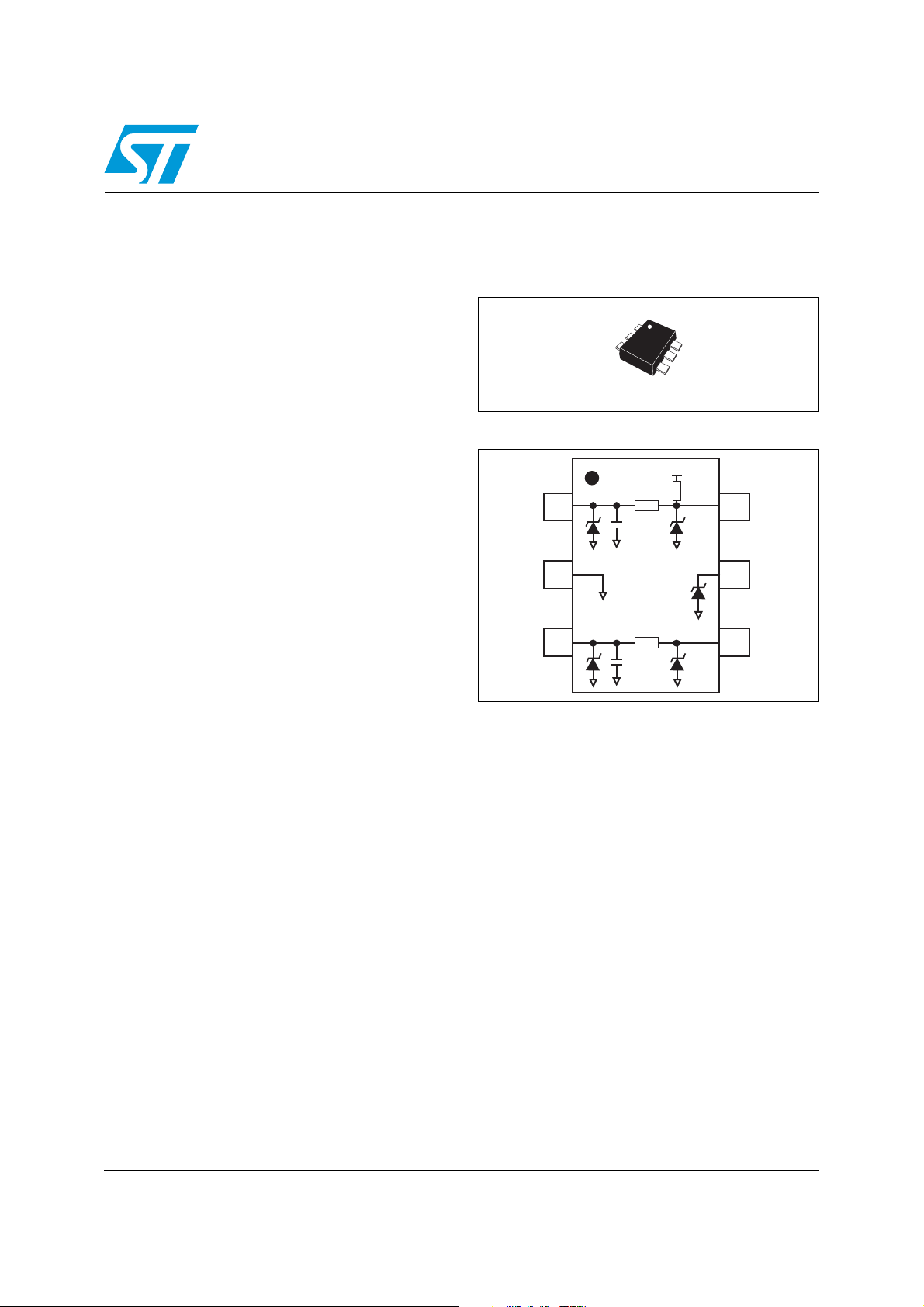
USBUF01P6
SOT-666IP
Figure 1. Functional diagram (top view)
3.3 V
Rp
D1
GND
D2
Rt
Ct
Rt
Ct
D4
3.3 V
D3
Complies with the following standards:
Description
■ IEC 61000-4-2 level4:
– 15 kV (air discharge)
– 8 kV (contact discharge)
■ MIL STD 883E-Method 3015-7:
– Class 3, C = 100 pF, R = 1500 Ω
– 3 positive strikes, 3 negative strikes
(F = 1 Hz)
Applications
EMI Filter and line termination for USB upstream
ports on:
■ USB Hubs
■ PC peripherals
February 2010 Doc ID 9883 Rev 7 1/9
The USB specification requires upstream ports to
be terminated with pull-up resistors from the D+
and D- lines to V
. For the implementation of
bus
USB systems, the radiated and conducted EMI
should be kept within the required levels as stated
by the FCC regulations. In addition to the
requirements of termination and EMC
compatibility, the computing devices are required
to be tested for ESD susceptibility.
The USBUF01P6 provides the recommended line
termination while implementing a low pass filter to
limit EMI levels and providing ESD protection
which exceeds IEC 61000-4-2 level 4 standard.
The device is packaged in a SOT-666, which is
the smallest available lead-frame package (45%
smaller than the standard SOT323).
TM: IPAD is a trademeark of STMicroelectronics
www.st.com
9

Characteristics USBUF01P6
1 Characteristics
Table 1. Absolute maximum rating (T
Symbol Parameter Value Unit
amb
= 25 °C)
IEC 61000-4-2 air discharge
V
ESD discharge
PP
IEC 61000-4-2 contact discharge
MIL STD 883E - Method 3015-7
Junction temperature 150 °C
T
j
T
Table 2. Electrical characteristics (T
Symbol Parameter
V
V
Storage temperature range -55 to +150 °C
stg
Maximum lead temperature for soldering during 10 s at 5 mm for case 260 °C
T
L
T
Operating temperature range -40 to + 85 °C
op
= 25 °C)
amb
I
Stand-off voltage
V
I
I
RM
Breakdown voltage
BR
Clamping voltage
CL
Leakage current
RM
Peak pulse current
PP
V
V
CL
BR
I
F
V
V
RM
F
I
RM
αT Voltage temperature coefficient
Forward voltage drop
V
F
Slope = 1/Rd
I
PP
Rd Dynamic resistance
Symbol Test conditions Min. Typ. Max. Unit
± 16
± 9
± 25
kV
V
V
I
BR
I
RM
R
t
R
p
C
t
= 1 mA 6 10 V
R
VRM = 3.3 V per line 500 nA
Tolerance ± 10% 33 Ω
Tolerance ± 10% 1.5 kΩ
Tolerance ± 20% 47 pF
2/9 Doc ID 9883 Rev 7

USBUF01P6 Technical information
t
t
2 Technical information
Figure 2. USB standard requirements
3.3V
1.5k
Rt
D+
D-
3.3V
1.5k
D+
D-
Ct
Rt
Ct
Rt
Ct
Rt
Ct
Full-speed USB
Transceiver
Hub 0 or
Full-speed function
Low-speed USB
Transceiver
Hub 0 or
Low-speed function
Full-speed or
Low-speed USB
Transceiver
Host or
Hub port
Full-speed or
Low-speed USB
Transceiver
Host or
Hub port
2.1 Application example
Rt
Ct
Ct
Ct
Ct
D+
Rt
15k
15k
Rt
Rt
15k
15k
Twisted pair shielded
Zo = 90ohms
D-
5m max
FULL SPEED CONNECTION
D+
Untwisted unshielded
3m max
D-
LOW SPEED CONNECTION
Figure 3. Implementation of ST solutions for USB ports
Downstream port
D+
Gnd
D-
Host/Hub USB por transceivert
Downstream port
D+
Gnd
D-
Host/Hub USB por transceivert
D+ in
Gnd
D- in
D+ in
Gnd
D- in
USBDF01W5
Rt
Ct
Rd
Rd
Ct
Rt
USBDF01W5
Rt
Ct
Rd
Rd
Ct
Rt
D+ out
D-
D- out
D+
D-
CABLE
D+
FULL SPEED CONNECTION
D+ out
D-
D- out
D+
D-
CABLE
D+
LOW SPEED CONNECTION
USBUF01P6
Ct
USBUF01P6
Ct
D2
Rt
D3
D2
Rt
D3
GND
3.3V
GND
3.3V
Upstream por
D+
D1
Ct
Rt
3.3 V
Rp
D4
Peripheral transceiver
D-
Upstream por
D+
D1
Ct
Rt
3.3 V
Rp
D4
Peripheral transceiver
D-
Doc ID 9883 Rev 7 3/9
Technical information USBUF01P6
2.1.1 EMI filtering
Current FCC regulations require that class B computing devices meet specified maximum
levels for both radiated and conducted EMI.
● Radiated EMI covers the frequency range from 30 MHz to 1 GHz.
● Conducted EMI covers the 450 kHz to 30 MHz range.
For the types of device compliant with the USB standard, the most difficult test to pass is
usually the radiated EMI test. For this reason the USBUF01P6 device aims to minimize
radiated EMI.
The differential signal (D+ and D-) of USB devices does not contribute significantly to
radiated or conducted EMI because the magnetic field of each conductor cancels out the
other.
The inside of a PC product is very noisy and designers must minimize noise coupling from
the different sources. D+ and D- must not be routed near high speed lines (clock spikes).
Induced common mode noise can be minimized by running pairs of USB signals parallel to
each other and running grounded guard trace on each side of the signal pair from the USB
controller to the USBUF device.
If possible, locate the USBUF device physically near the USB connectors. Distance between
the USB controller and the USB connector must be minimized.
The 47 pF (C
) capacitors are used to divert high frequency energy to ground and for edge
t
control, and are placed between the driver chip and the series termination resistors (R
Both C
and Rt should be placed as close to the driver chip as is practicable.
t
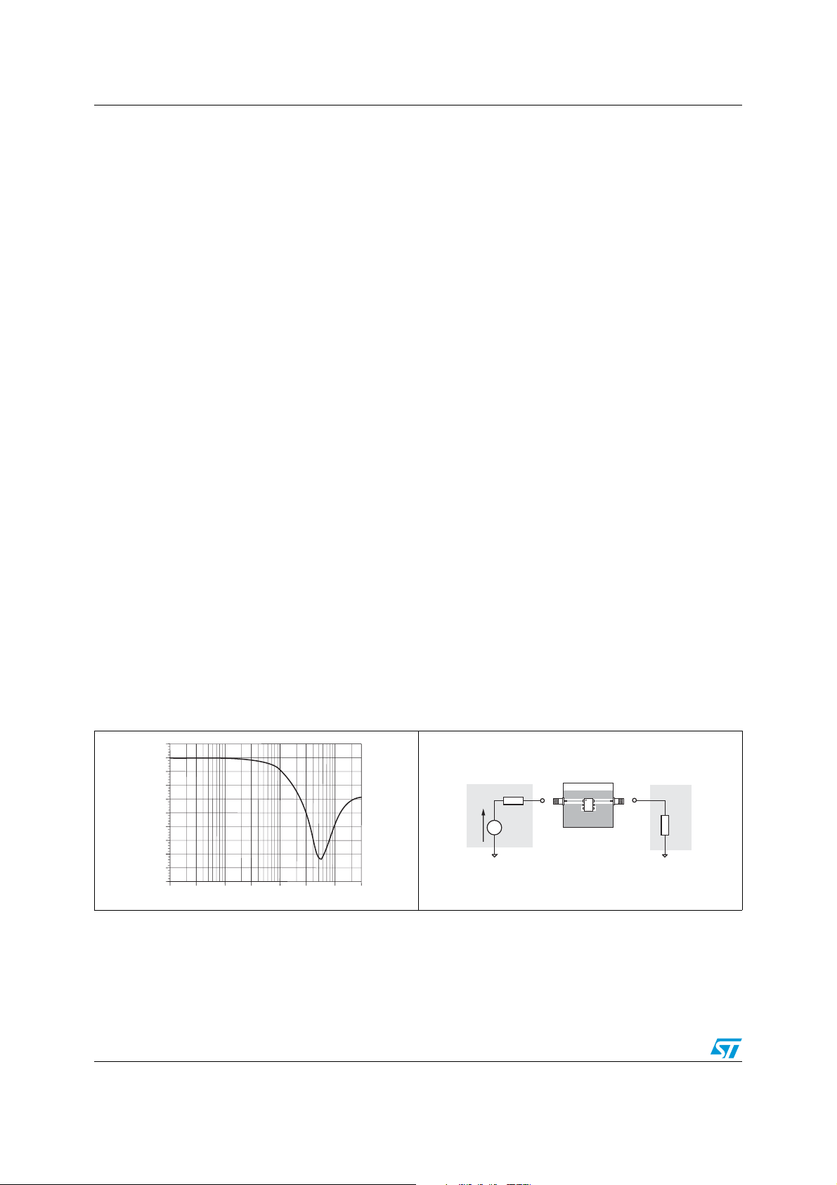
The USBUF01P6 ensures a filtering protection against electro-magnetic and radio
frequency Interference thanks to its low-pass filter structure. This filter is characterized by
the following parameters:
● Cut-off frequency
● Insertion loss
● High frequency rejection.
Figure 4. USBUF01P6 typical attenuation
curve
0.00
dB
-
-2.50
-
-5.00
-
-7.50
-
-10.00
-
-12.50
-
-15.00
-
-17.50
-
-20.00
-
-22.50
-
-25.00
1.0M 3.0M 10.0M 30.0M 100.0M 300.0M 1.0G 3.0G
f/Hz
Figure 5. Measurement configuration
50
Ω
Vg
TEST BOARD
UUx
50
).
t
Ω
4/9 Doc ID 9883 Rev 7

USBUF01P6 Technical information
2.1.2 ESD protection
In addition to the requirements of termination and EMC compatibility, computing devices are
required to be tested for ESD susceptibility. This test is described in IEC 61000-4-2 and is
already in place in Europe. This test requires that a device tolerates ESD events and
remains operational without user intervention.
The USBUF01P6 is particularly optimized to perform ESD protection. ESD protection is
based on the use of device which clamps at:
V
CLVBRRdIPP
This protection function is split into 2 stages. As shown in Figure 6. The ESD strikes are
clamped by the first stage S1 and then its remaining overvoltage is applied to the second
stage through the resistor R
Figure 6. USBUF01P6 ESD clamping behavior
⋅+=
. Such a configuration makes the output voltage very low.
t
V
PP
ESD Surge
Rg
S1
Rd
V
BR
Rt
Vinput
Voutput
S2
Rd
V
BR
USBUF01P6
Figure 7. Measurement board
ESD
SURGE
15kV
Air
Discharge
TEST BOARD
U
Vin Vout
To have a good approximation of the remaining voltages at both V
we give the typical dynamical resistance value R
hypothesis: R
Vinput
Voutput
R
-----------------------------------------------=
, Rg>Rd and R
t>Rd
gVBRRdVg
R
tVBRRd
--------------------------------------------------------- -=
⋅+⋅
R
g
R
t
load>Rd
, gives these formulas:
Vinput⋅+⋅
. Taking into account the following
d
input
Rload
Device
to be
protected
and V
output
stages,
The calculation done for V
and R
= 2 Ω (typ.) gives:
d
V
= 55.48 V
input
V
= 10.36 V
output
= 8 kV, Rg = 330 Ω (IEC 61000-4-2 standard), VBR= 7 V (typ.)
g
Doc ID 9883 Rev 7 5/9
Technical information USBUF01P6
This confirms the very low remaining voltage across the device to be protected. It is also
important to note that in this approximation the parasitic inductance effect was not taken into
account. This could be a few tenths of volts during a few ns at the V
effect is not present at the V
side due the low current involved after the resistance Rt.
output
side. This parasitic
input
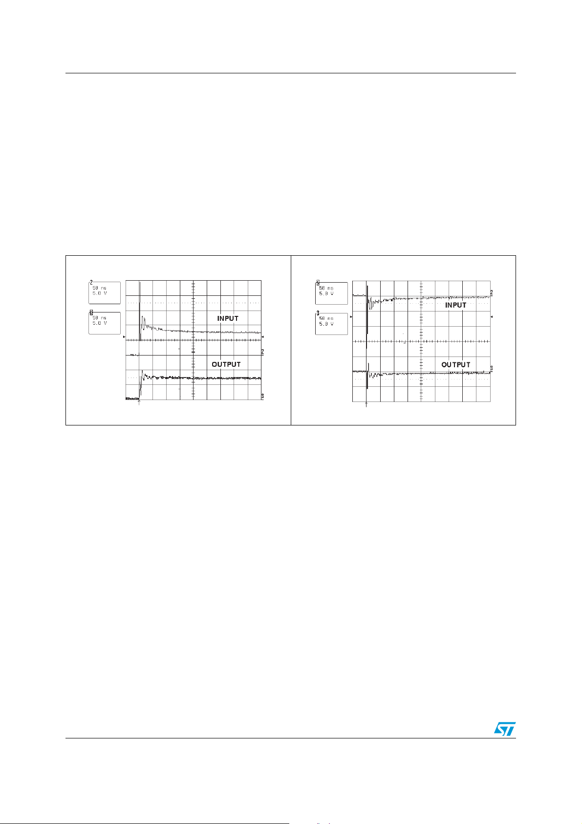
The measurements done hereafter show very clearly (Figure 8 and Figure 9) the high
efficiency of the ESD protection:
● No influence of the parasitic inductances on V
● V
clamping voltage very close to VBR (breakdown voltage) in the positive way and
output
-V
(forward voltage) in the negative way
F
Figure 8. Remaining voltage at both stages
S1 (V
) and S2 (V
input
output
) during
positive ESD surge
Figure 9. Remaining voltage at both stages
stage
output
S1 (V
) and S2 (V
input
negative ESD surge
output
) during
Note: The USBUF01P6 acts not only for positive ESD surges but also for negative ones. For these
kinds of disturbances it clamps close to ground voltage as shown in Figure 9.
6/9 Doc ID 9883 Rev 7
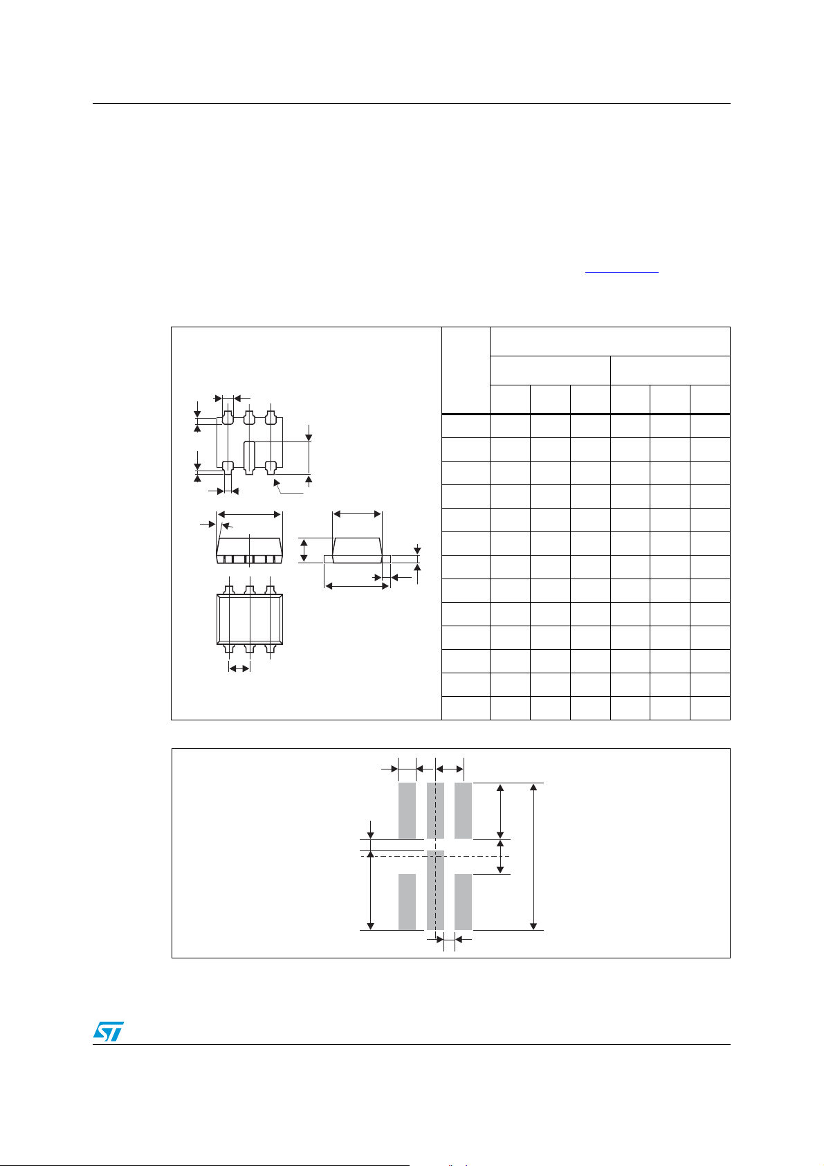
USBUF01P6 Package information
3 Package information
● Epoxy meets UL94, V0
● Lead-free package
In order to meet environmental requirements, ST offers these devices in different grades of
ECOPACK
specifications, grade definitions and product status are available at: www.st.com
ECOPACK
Table 3. SOT-666IP dimensions
®
packages, depending on their level of environmental compliance. ECOPACK®
®
is an ST trademark.
.
Dimensions
angle
Ref.
b1
L1
L4
L3
b
Pin 1
D
E1
A 0.53 0.57 0.60 0.021 0.22 0.024
A3 0.13 0.17 0.18 0.005 0.007 0.007
b 0.17 0.25 0.007 0.009
b1 0.27 0.34 0.011 0.013
D 1.50 1.66 1.70 0.059 0.065 0.067
A
L2
E
A3
E 1.50 1.65 1.70 0.059 0.065 0.067
E1 1.10 1.20 1.30 0.043 0.047 0.051
e0.50 0.020
Millimeters Inches
Min. Typ. Max. Min. Typ. Max.
L1 0.11 0.19 0.26 0.004 0.007 0.010
L2 0.10 0.23 0.30 0.004 0.009 0.012
e
L3 0.05 0.10 0.002 0.004
L4 0.83 0.033
angle° 8 10 12 8 10 12
Figure 10. SOT-666IP footprint (dimensions in mm)
0.30
0.21
1.40
Doc ID 9883 Rev 7 7/9
0.50
0.20
0.99
0.62
2.60

Ordering information USBUF01P6
3.1 Mechanical specifications
Lead plating Mat tin
Lead plating thickness 7 µm min, 20 µm max
Lead coplanarity 10 µm max
Body material Molded epoxy
Flammability UL94, V0
4 Ordering information
Table 4. Ordering information
Order code Marking Package Weight Base qty Delivery mode
USBUF01P6 U SOT-666IP 2.9 mg 3000 Tape and reel
5 Revision history
Table 5. Document revision history
Date Revision Changes
September-2003 1 First issue.
01-Jun-2004 2 SOT-666 Internal Pad version package change.
08-Jun-2005 3 Minor format changes; no content changed.
10-Mar-2006 4
16-Aug-2006 5 Updated SOT-666IP package dimensions in Table 3.
29-Aug-2006 6
18-Feb-2010 7
Footprint and dimension graphic improved in packaging
information. Ecopack statement added. Reformatted to
current standard.
Typing error in table 2 on page 2: change W and kW unit
to Ω and kΩ unit.
Updated GND pin annotation in Figures 1 and 3. Added
pin numbering indication to illustration and updated
dimension values in Ta bl e 3 . Updated mechanical
specifications in Section 3.1.
8/9 Doc ID 9883 Rev 7

USBUF01P6
Please Read Carefully:
Information in this document is provided solely in connection with ST products. STMicroelectronics NV and its subsidiaries (“ST”) reserve the
right to make changes, corrections, modifications or improvements, to this document, and the products and services described herein at any
time, without notice.
All ST products are sold pursuant to ST’s terms and conditions of sale.
Purchasers are solely responsible for the choice, selection and use of the ST products and services described herein, and ST assumes no
liability whatsoever relating to the choice, selection or use of the ST products and services described herein.
No license, express or implied, by estoppel or otherwise, to any intellectual property rights is granted under this document. If any part of this
document refers to any third party products or services it shall not be deemed a license grant by ST for the use of such third party products
or services, or any intellectual property contained therein or considered as a warranty covering the use in any manner whatsoever of such
third party products or services or any intellectual property contained therein.
UNLESS OTHERWISE SET FORTH IN ST’S TERMS AND CONDITIONS OF SALE ST DISCLAIMS ANY EXPRESS OR IMPLIED
WARRANTY WITH RESPECT TO THE USE AND/OR SALE OF ST PRODUCTS INCLUDING WITHOUT LIMITATION IMPLIED
WARRANTIES OF MERCHANTABILITY, FITNESS FOR A PARTICULAR PURPOSE (AND THEIR EQUIVALENTS UNDER THE LAWS
OF ANY JURISDICTION), OR INFRINGEMENT OF ANY PATENT, COPYRIGHT OR OTHER INTELLECTUAL PROPERTY RIGHT.
UNLESS EXPRESSLY APPROVED IN WRITING BY AN AUTHORIZED ST REPRESENTATIVE, ST PRODUCTS ARE NOT
RECOMMENDED, AUTHORIZED OR WARRANTED FOR USE IN MILITARY, AIR CRAFT, SPACE, LIFE SAVING, OR LIFE SUSTAINING
APPLICATIONS, NOR IN PRODUCTS OR SYSTEMS WHERE FAILURE OR MALFUNCTION MAY RESULT IN PERSONAL INJURY,
DEATH, OR SEVERE PROPERTY OR ENVIRONMENTAL DAMAGE. ST PRODUCTS WHICH ARE NOT SPECIFIED AS "AUTOMOTIVE
GRADE" MAY ONLY BE USED IN AUTOMOTIVE APPLICATIONS AT USER’S OWN RISK.
Resale of ST products with provisions different from the statements and/or technical features set forth in this document shall immediately void
any warranty granted by ST for the ST product or service described herein and shall not create or extend in any manner whatsoever, any
liability of ST.
ST and the ST logo are trademarks or registered trademarks of ST in various countries.
Information in this document supersedes and replaces all information previously supplied.
The ST logo is a registered trademark of STMicroelectronics. All other names are the property of their respective owners.
© 2010 STMicroelectronics - All rights reserved
STMicroelectronics group of companies
Australia - Belgium - Brazil - Canada - China - Czech Republic - Finland - France - Germany - Hong Kong - India - Israel - Italy - Japan -
Malaysia - Malta - Morocco - Philippines - Singapore - Spain - Sweden - Switzerland - United Kingdom - United States of America
www.st.com
Doc ID 9883 Rev 7 9/9
 Loading...