

Page 1
USB Power Delivery and Type-C
Overview
Product Portfolio Solution
Architecture
Page 2
USB Type-C Overview
USB Power Delivery specification introduces USB Type-C receptacle, plug and cable; they provide a
smaller, thinner and more robust alternativ e to existing USB interconnect. Main features are:
• Enable new and exciting host and device form-factors where size, industrial design and style are
important parameters
• Work seamlessly with existing USB host and device silicon solutions
• Enhance ease of use for connecting USB devices with a focus on minimizing user confusion for
plug and cable orientation
Page 3
USB Type-C Overview
Type-C Features
• Enable new and exciting host and device form-factors where size, industrial design and style are
important parameters
• Work seamlessly with existing USB host and device silicon solutions
• Enhance ease of use for connecting USB devices with a focus on minimizing user confusion
for plug and cable orientation
• Simple Power Delivery implementation (BMC)
Mode of Operation
USB 2.0 5 V 500 mA
USB 3.1 5 V 900 mA
USB BC 1.2 5 V Up to 1.5 A Legacy charging
USB Type-C @ 1.5 A 5 V 1.5 A Supports high power devices
USB Type-C @ 3.0 A 5 V 3 A Supports higher power devices
USB PD
Nominal
Voltage
Configurable
up to 20 V
Maximum
Current
Configurable
up to 5 A
Notes
Default current, based on definitions in the base
specifications
Directional control and power level management
Page 4
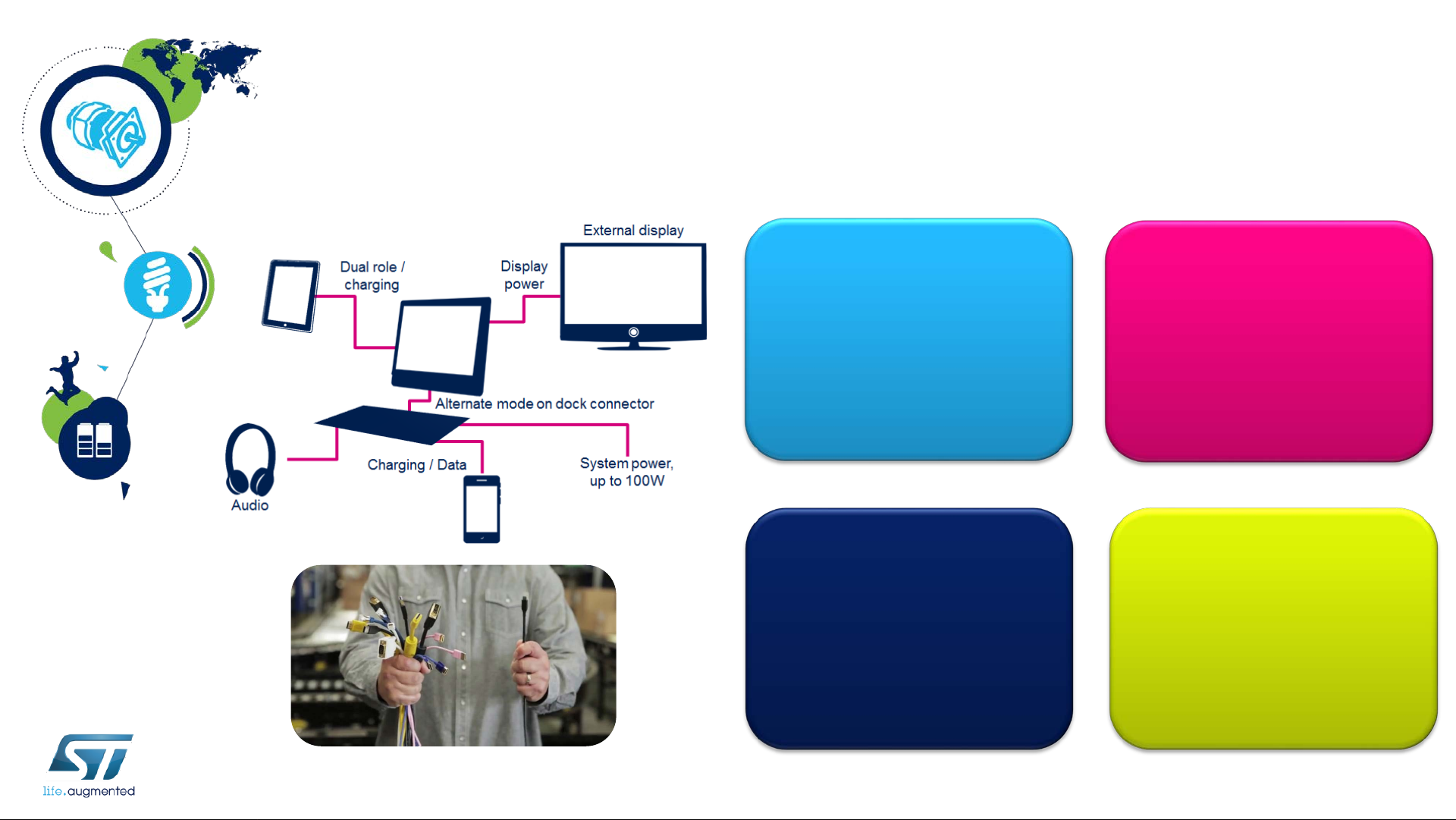
The Re-Evolution of USB
USB has evolved fr om a data interface capable of suppl ying limited power
to a primary provider of power with a data interface
Power
Delivery
Type-C
Alternate
Mode
USB IF
More Power with USB Power Delivery (100W)
More Flexibility with a new reversible USB-C connector
More Protocols
(Display Port, HDMI, VGA, Ethernet…)
More Speed with USB 3.1 (10 Gbit/s)
Page 5
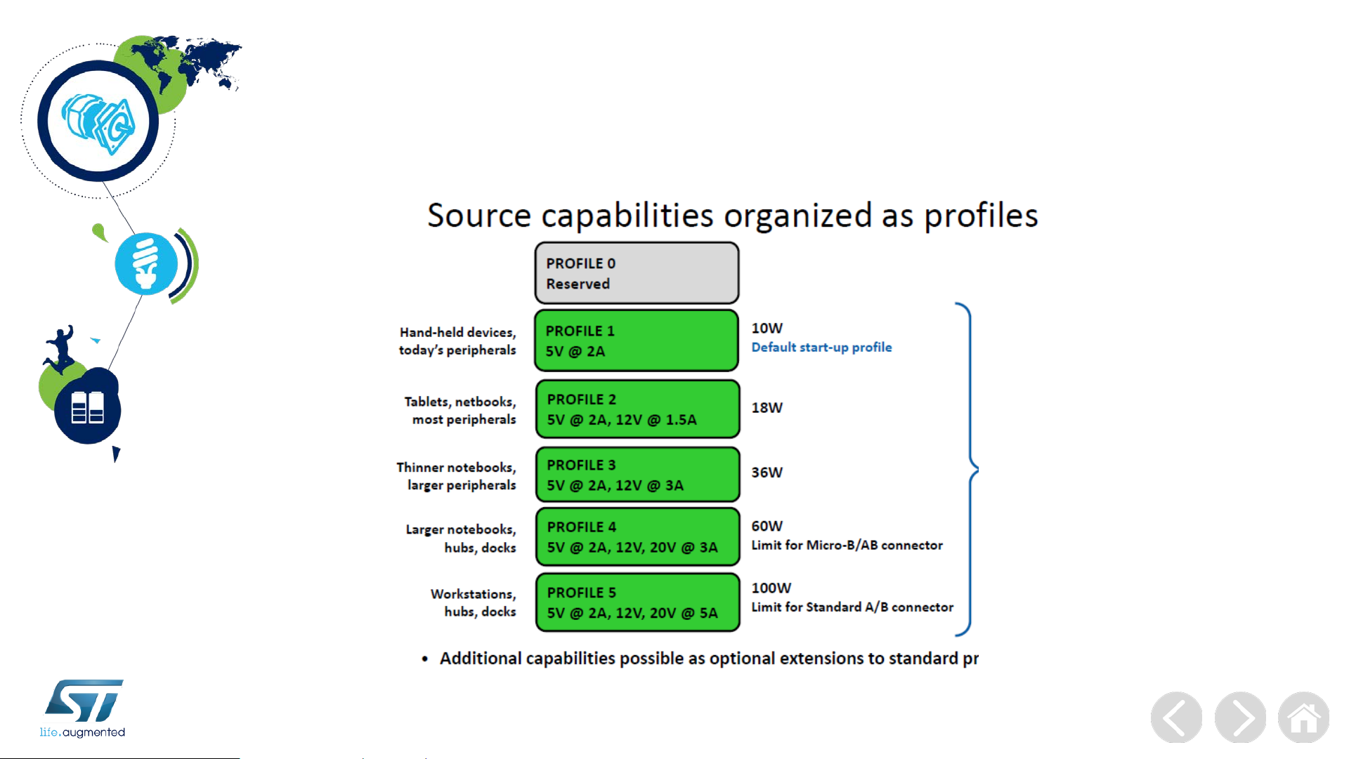
USB PD Power Profiles
as of today …. per USB PD release 2.0
Page 6
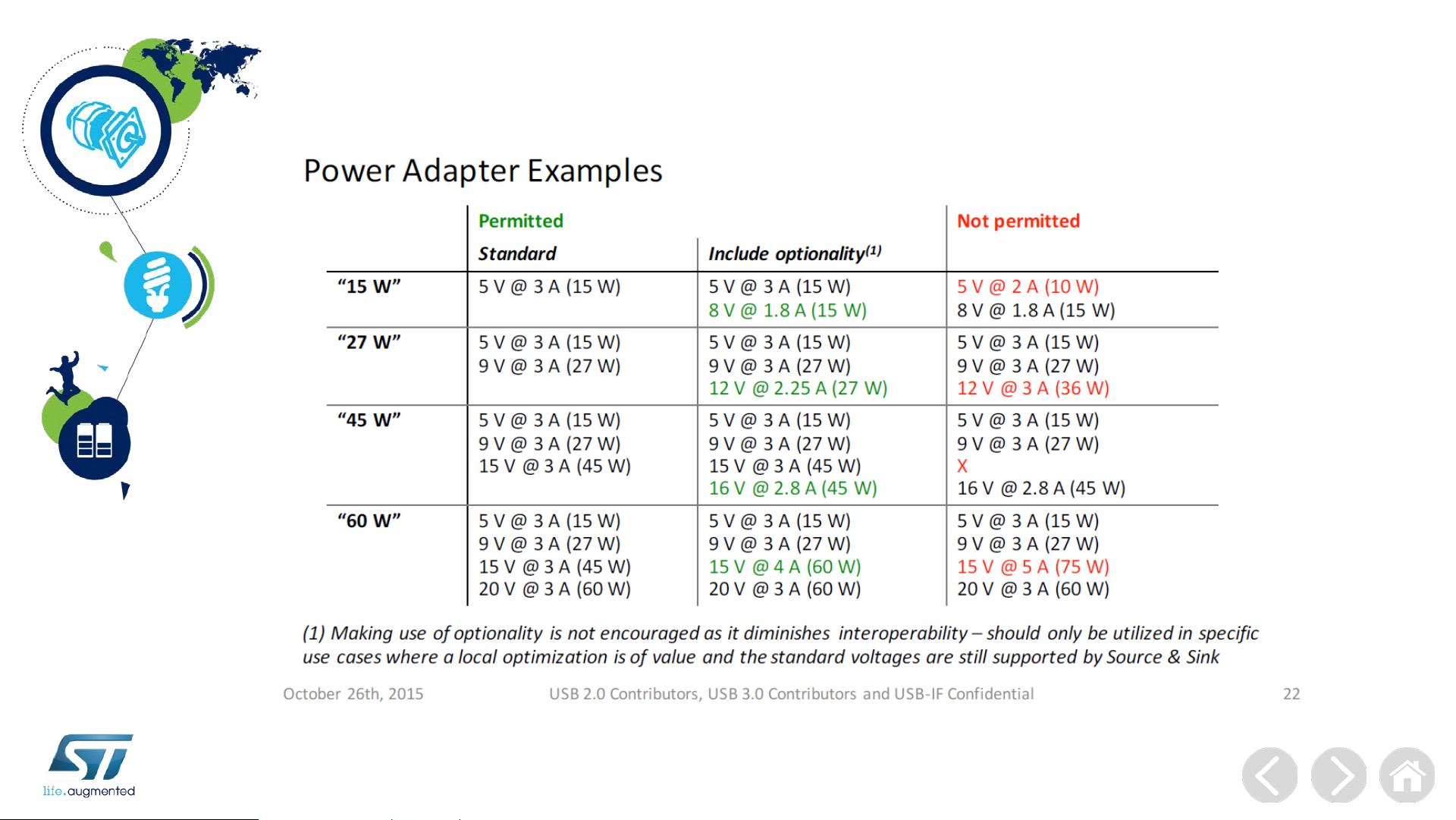
USB PD New Profiles proposal
Page 7
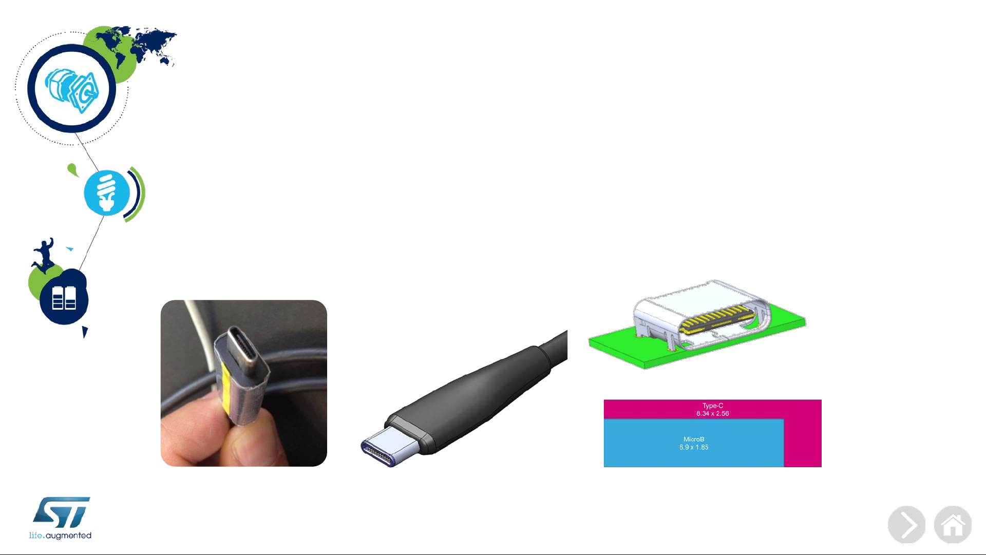
Type-C Pin Outs Functions
Receptacle
High Speed Data Path
(RX for USB 3.1, or reconfigured
in Alternate Mode)
A1 A2 A3 A4 A5 A6 A7 A8 A9 A10 A12 A12
GND
GND
B12 B11 B10 B9 B8 B7 B6 B5 B4 B3 B2 B1
Secondary
TX1+ TX1- V
RX1+ RX1- V
Cable Bus
BUS
BUS
CC1 D+ D- SBU1 V
SBU2 D- D+ CC2 V
USB 2.0
Interface
Cable
High Speed Data Path
(TX for USB 3.1, or reconfigured
in Alternate Mode)
BUS
BUS
RX2- RX2+
TX2- TX2+
GND
GND
Configuration Channel
Bus
Power
Ground
Two pins on the USB Type-C receptacle, CC1 and CC2,
are used in the discovery, configuration and management
of connections across USB type-C cable
Page 8
Type-C Pin Outs Functions
Plug
High Speed Data Path
(RX for USB 3.1, or reconfigured
in Alternate Mode)
A12 A11 A10 A9 A8 A7 A6 A5 A4 A3 A2 A1
GND
GND
B1 B2 B3 B4 B5 B6 B7 B8 B9 B10 B11 B12
Secondary
RX2+ RX2- V
TX2+ TX2- V
Cable Bus
BUS
BUS
SBU1 D- D+ CC V
V
CONN
USB 2.0
Interface
SBU2 V
Cable
High Speed Data Path
(TX for USB 3.1, or reconfigured
in Alternate Mode)
BUS
BUS
TX1- TX1+
RX1- RX1+
GND
GND
Configuration Channel
Bus
Power
Ground
On a standard USB Type-C cable, only a single CC wire within each plug is
connected through the cable to establish signal orientation
The other CC pin is repurposed as V
CONN
for powering electronics
Also, only one set of USB 2.0 D+/D- wires are i mplemented
Page 9
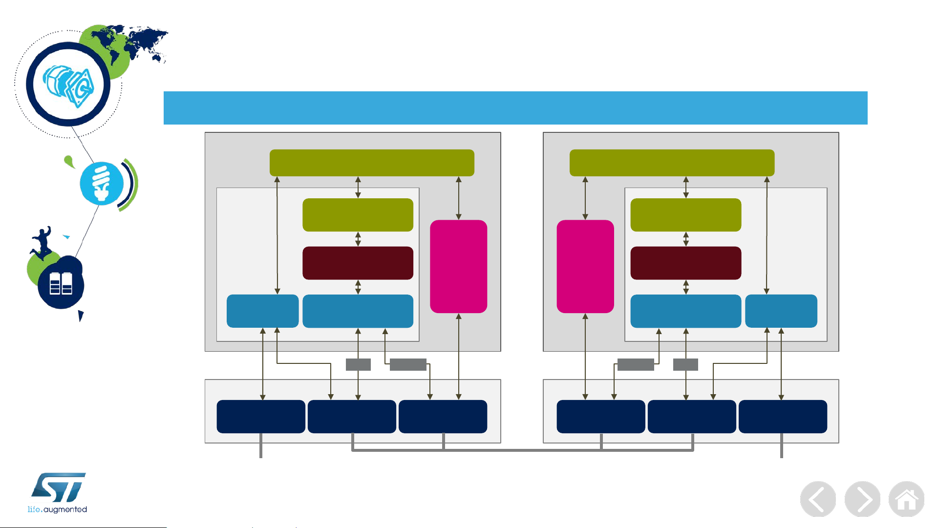
Architecture
Architecture and key words
Provider
Source
port
Cable
Detection
USB Port
T ype A/B Plug
identification
Device Policy Manager
Policy Engine
Protocol Layer
Physical Layer
BFSKBMC
CC
(Type-C only)
VBUS
Power
Source(s)
V
BUS
Power
Sink
VBUS
Device Policy Manager
Policy Engine
Protocol Layer
Physical Layer
BFSK BMC
CC
(Type-C only)
Consumer
Sink
port
Cable
Detection
USB Port
T ype A/B Plug
identification
CC
Communication acr oss the channel uses BiphaseMark Coding (BMC) over CC in Type C connector
Page 10
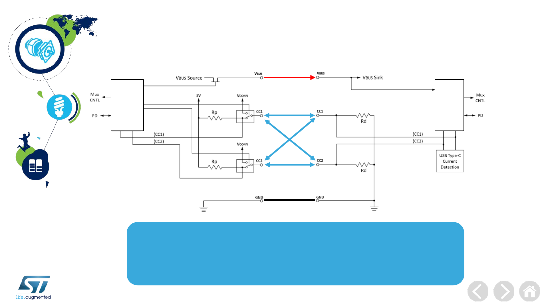
USB Type-C CC Connections
DFP -
Source
Connection
Detection
and muxes
control
4 possible CC
configurations
UFP - Sink
Connection
Detection
• Detect attach/detach of USB ports, e.g. a DF P to a UFP
• Resolve cable orientation and twist connections to establish USB data bus routing
• Establish DFP and UFP roles between two attached ports
• Discover and configure VBUS
• USB Power Delivery Communication
Page 11

USB PD Stack & Policy
Policies
System Policy Manager (system
wide) is optional. It monitors and
controls System Policy between
various Providers and Consumers
connected via USB.
Device Policy Manager (one per
Provider or Consumer) provides
mechanisms to monitor and control
the USB-PD within a particular
Provider or Consumer. It enables
local policies to be enforced across
the system by communication with
the System Policy Manager.
Policy Engine (one per Source or
Sink Port) interacts directly with the
Device Policy Manager in order to
determine the present local policy
to be enforced.
USB Host
System Policy
Manager
USB hub tree
(optional)
USB PD device
USB interface
(optional)
Device Policy
Manager
Policy Engine
Protocol Layer
Physical Layer
Protocol Layer
The Protocol Layer forms the messages
used to communicate information between a
pair of ports. It receives inputs from the
Policy Engine indicating which messages to
send and indicates the responses back to
the Policy Engine
Physical Layer
It is responsible for sending and receiving
messages across either the V
wire. It consists o f a transce i v er th at
superimposes a signal (BFSK on V
BMC on CC) on the wire.
It is responsible for managing data on the
wire and for collision avoidance and detects
errors in the messages using a CRC
BUS
or CC
BUS
or
V
BUS
/ CC
Page 12

Product Portfolio
A complete offer to “lean in” USB PD Ecosystem
SuperSpeed
Switch
Host, USB
3.1
Controller
Access Point
(optional)
USB Power Delivery
Controller
Power Management
PHY - Type-C
interface
Protections
Type-C
connector
Page 13

Power Source Building Blocks
High V oltage Low Voltage
Profile 1-2-3
Flyback
Controller:
STCH02
Power
MOSFET
main
transformer
pulse
transformer
optocoupler
communication
•
It covers profile 1-2-3 from 5W to 45W
• High Efficiency
• Low EMI design: intelligent Jitter for EMI suppression
Rectifier
CC/CV
SEA01
Feedback
Network
Selection
USB PD
Interface IC
Multi Port case:
Post regulation
for each port
DC/DC
USB PD
Post
Interface IC
regulation
Page 14

STCH02
Primary Side Controller: Adapters up to 45W
Features
• Proprietary Constant current output regulation (CC)
with no opto-coupler
• 700V embedded HV start-up circuit
• Quasi-resonant (QR) Zero Voltage Sw itching (ZVS)
operation
• Valley skipping at medium-light load and advanced
burst mode operation at no-load for under 10mW
consumption
• Accurate adjustable output OVP
Benefits
SO8
• Low part count. BOM reduction thanks to an
extensive features integration
• Exceeding 5 stars: No-Load power < 10mW
• HV start-up zero power consumption
• Advanced burst-mode operati on
• Flexibility: suitable for adapters from 5W to 40W
• High Efficiency
• Low EMI design: intelligent jitter for EMI
suppression
Page 15

Profile 4, 5
Power Source Building Blocks
High V oltage
PFC
L6563H
LLC
L6699
Power
MOSFET
PFC-LLC
main
transformer
optocoupler
Low Voltage
Synchrounous
Rectification
SRK2001
Power MOSFET
CC/CV
SEA01
Post Regulation
DC/DC
Post regulation
USB PD
Interface IC
1 per port
Integrated
New
solution
STCMB1
Page 16

Transition Mode PFC controller
Features
• 700V High Voltage Start-up circuit
• Fast bidirectional input voltage feedforward
• Adjustable OVP
• AC Brownout Detection
• Tracking boost function
• Inductor saturation protection
• Proprietary THD optimizer circuit
• Interface for cascaded converters
• -600mA/+800mA gate driver
L6563H
Datasheet : available on www.st.com
SO16
• Low steady state ripple and current distortion
with limited undershoot or overshoot of the preregulator’s output thanks to new input voltage
feed-forward implementation
• Reduced THD of the current
• High reliability thanks to a full set of protections
• HV start-up significantly reduces consumption
compared to standard discrete circuit solutions
• Facilitated cooperation with cascaded DC-DC
converter thanks to several power management
& housekeeping functions
Page 17

L6699
High power adapters 90W to 250W
Series-resonant half-bridge topology
Datasheet : available on www.st.com
Features
• Self adjusting adaptive dead time
• Anti-capacitive mode protection
• Two-level OCP
• Frequency shift
• Immediate shutdown
• Safe-start procedure
• Burst-mode operation at light load
• Brown-out protection
• Interface with PFC controller
Benefits
• High efficiency:
• Reduced internal consump tion (Iq=1mA)
• Adaptive dead time allows design optimizat ion to
achieve ZVS with lower magnetizing current
SO16N
• Improved reliability and lifetime thanks to anticapacitive protection and smooth start-up circuit
• Reduced audible noise when entering burstmode operation thanks to smooth restart feature
Page 18

USB-PD
Power MOSFET product families
800V-1500V
K5
Flyback
600V-650V
M2
Price/Performance Premium efficiency
Flyback/PFC/LLC
M6
40-120V
F7
Synch Rec
Page 19

Flyback Architecture
VHV PowerMOSFETs
Features
Outstanding Form Factor
STL8N80
800V, 950mOhm, 13nC
PowerFLAT5x6
• Unmatched R
800-950V-1050V
• Ultra-Low Q
• Extremely low thermal resistance
• High quality & reliability
• Lower on-state conduction losses
• Best switching losses
• High efficiency with lower design complexity
• Ultra small Form factor
Part Number B
at very high BVDSS
DS(on)
and high switching speed
G
Benefits
Product range example
VDss
R
DS(on)
I
D
STB13N80K5 800V 0.45Ω 12A
STD8N80K5 800V 0.95Ω 6A
STD9N80K5 800V 0.90Ω 7A
Page 20

Power MOSFET
PFC & LLC Architecture
Features
Product range example
PFC V
STF24N60M2 600V 0.190Ω 18A
STF25N60M2-EP 600V 0.188Ω 18A
STF20N60M2-EP 600V 0.278Ω 13A
LLC V
STF9N60M2 600V 0.750Ω 5.5A
STF15N60M2-EP 600V 0.378Ω 11A
STFI11N60M2-EP
(e.s.available)
LLC V
DSS
DSS
600V 0.595Ω 8.0A
DSS
R
DS(on)
R
DS(on)
R
DS(on)
• Up to 30% lower Q
(equivalent die size)
• 400 – 700V BV
DSS
vs main competition
G
rated
• Back-to-Back G-S Zener protected
I
D
Benefits
PFC
Performance
I
D
• Reduced switching losses
• Enhanced immunity vs ESD & Vgs spikes
• Technologies dedicated to specific topology
Product range example
LLC
Performance
I
D
STL24N60
600V, 210mΩ, 28nC
PowerFLAT8x8
STF9N60M6 600V 0.750Ω
STF10N60M6 600V 0.600Ω
STF13N60M6 600V 0.380Ω
ES April ‘16
ES April ‘16
ES April ‘16
LLC
Premium
Page 21

Power MOSFETs
Synchronous Rectification
Features
Part Number Voltage Ron Current
STL260N4LF7 40V <1.1mΩ 5.5A
STL200N45LF7 40V <1.8mΩ 11A
• Very low R
• Proper C
• Low V
• LL Vth
OSS
and QRRwith soft recovery body-drain diode
SD
DS(on)
;
;
Benefits
• Efficiency improvement due low conduction losses and
to static and dynamic diode ones, minimized switching
noise and Vds spike at turn OFF
• Easy driving features
Page 22

Protections
ESD/CMF/ECMF
High flexibility for the Designers needs to find best compatibilities
• Robustness: Surge capability up to 25kV and low clamping
ESD Protection
ESD + CMF
ECMF = ESD + CMF integrated
• Flexibility & Integration: Single or multi lines products
• Transparency : High bandwidth for high speed signals
• High quality of protection
• Unique filtering shape capabilities
• Serial Interface: U SB2.0/3.0 , MIPI,D P, HDMI
• Filters radiated noise and limits antenna de-sense.
•
High quality of protection
•
High integration: 1mm2 / 2 differentia l lines
• Serial Interface: U SB2.0/3.0 , MIPI,D P, HDMI
• Filters radiated noise and limits antenna de-sense
Page 23

Controller & Interface
Value proposit ion: offer flexible and scalable solutions for
designers
USB PD Controller
MCU Based
STM32
• FW USB PD Stack
• Adaptability versus USB PD
specification new release
• PHY-Type-C interface
companion chip
• Market proven solution
PHY -Type-C Inter face
STUSB16
• Dual Role Ty pe-C Interface
with BMC
• Dual role capability
• Configurable start-up profiles
• Interface with external MCU
2
through I
• Accessory support
C
USB PD Hard Coded
Controller
STUSB4x
• HW USB PD Stack
• Flexible HW-SW partitioning
• Autorun or Micro based
• Easy Dead Battery Support
• P2P with PHY-Type-C
interface
Page 24

MCU Overview:
STM32F0 HW resources
• Transmission uses : TIM14, SPI1, DMA, GPIO
• Reception uses : TIM3, DMA, 1 comparator
• TIM2 is used to time-schedule tasks
• Embedded ADC to detect device on the CC bus
and perform power measurements
• CRC to evaluate message’s CRC
• Standard GP I/Os to control Vconn, Load switch,
Vbus discharge switch, Vout selection (primary
feedback…
Project Flash Memory RAM Memory
Provider only 25.5 kB 4.4 kB
Provider only (RTOS) 29.0 k B 7.3 kB
Provider/Consumer
DRP (RTOS)
30.2 kB 7.3 kB
Page 25

USB-PD Interface:
STUSB16xx
Features
• Dual Role T ype-C Interface w ith BMC
• Dual role capability
• Configurable star t-up profiles
• 600mA VCONN
• 120uA Idle current measured
• Interface with external M CU through I² C+I nterrupt
QFN-24 (4x4 mm)
Pin to pin compatibl e with STUSBxx family
https://www.st.com/usb-type-c
CSP
• Integrated V oltag e monitoring
• Integrated V
• Accessory support
• Dual Power supply:
• V
SYS =
• VDD[4.6V; 22V] (from V
discharge path
BUS
3.3V,
BUS
)
Benefits
• Low Pin count
• Integrated BMC transceiver
• Simple, Robust
• Configurable, Flexible
• Optimized for Portable applications
• P2P with STUSB4x
Page 26

USB-PD Type-C Solution
• AC/DC Multi-output 36W Converter
• Based on STCH02 QR controller
• Multiple Output voltages (5V, 9V, 12V)
• STM32 Embedded Software Solution
• to interface with USB-C connector
• to handle t
• cost ef
fective and popular 32bit Microcontroller
he USB Power Delivery protocol
• HW platform based on X-Nucleo Shield
Page 27

Block Diagram
NUCLEO +
MORPHO
CONNECTORS
Internal Power
Block
Power Connector
Analog
Front End
Type-C
Interface
NUCLEO + X-NUCLEO-USBPDM1
External Power
Supply Board
Modular
Approach
Page 28

Block Diagram: Features
Power Connector
V
CONN
V
Analog
Front End
& Cable Logic
CONN
Load Switch
Switch
Internal Supply
Bus Discharge
Role Setup
ESD
ESD
V
BUS
CCsCCs
Volt & Curr
Sensing
Receptacle
USB 2.0
USB 2.0
On board functionalities activable if not available on
external power s uppl y boar d.
USB 2.0 hooked to Type-C on Port 0, if available on
STM32.
Page 29

AC/DC 36W 5/9/12V
Iout
Iout
Efficiency and no Load Consumption
Load
100%
75%
50%
25%
Average
Input
voltage
115V
AC
230V
AC
Input voltage
115Vac 11mW
Efficiency @ 115Vac
[A] 5V
3.000 83.18% 85.17% 85.41%
2.250 80.61% 85.34% 85.53%
1.510 80.20% 84.71% 84.61%
0.750 80.92% 85.17% 81.67%
81.23% 84.45% 84.30%
Efficiency @ 10% Pout
5V
76.29% 76.68% 73.28%
73.09% 73.06% 70.54%
No load consumption
9V 12V
9V 12V
5V
Load
100%
75%
50%
25%
Average
Efficiency @ 230Vac
[A] 5V
3.000 82.42% 85.56% 86.35%
2.250 81.44% 84.65% 85.47%
1.510 80.65% 83.44% 84.08%
0.750 77.89% 80.36% 80.05%
80.60% 83.50% 84%
•
36W 5/9/12V board
9V 12V
230Vac 12mW
• Please note that the v al ues of effic iency are penali zed by the power los ses on s econd ar y rectifier diode.
• The efficiency can be improved around 4% usi ng synchr onous rectificat ion
Page 30

AC/DC 36W 5/9/12V
Schematic
Page 31

1
MCU + Discrete AFE Overview
STM32F0
• STM32 Embedded Software Solution to
interface with USB-C connector and to
handle the USB Power Delivery protocol.
USB-C & PD
FW
Hardware : Entry level Cortex-M0
based STM32F0 microcontroller series
GPI/Os
Discrete
Analog FE
CC1/CC2
with simple discrete Analog Front End
PHY
Embedded Software : USB-C & PD
Middleware
Best device for 2 ports management : STM32F051 in 48 pi n pack ag e
Best device for 1 port management : STM32F051/31 in 20/32 pin package
USB T y pe-C
connector
Page 32

X-NUCLEO-USBPDM1
• USB-C Power Deliv
ery expansion board
with two USB Type-C connectors for two
port management.
• Main features:
• Two Dual Role Ports
• Dedicated Power Connector to interface with
external Power Supply board providing different
profiles (up to 20V and 5A) and V
• On-board Power management able to provide
internal needed voltages from V
• Six debug LEDs
• USB 2.0 interface capability available on one port
CONN
BUS
• Compatible with STM32 Nucleo boards
• Equipped with ST morpho connectors
Page 33

X-NUCLEO-USBPDM1
Morpho connectors
Power Role Configuration Port 1
CC AFE and V
V
Port 1 Switch and discharge
BUS
Power Connector for external Power Source
Switch Port 1
CONN
User LEDs
Board Details
Power Role Configuration Port 0
CC AFE and V
V
Port 0 Switch and discharge
BUS
Switch Port 0
CONN
V
Current/Voltage sens ing Port 1
BUS
Type-C Receptacle Port 1
Connector for V
Load Port 1
BUS
Connector for V
V
Current/Voltage sens ing Port 0
BUS
Local Power Management
Type-C Receptacle Port 0 (USB2.0 Capability )
Load Port 0
BUS
 Loading...