

ST USBLC6-2 User Manual
查询USBLC6-2供应商
®
ASD
(Application Specific Devices)
MAIN APPLICATIONS
■ USB2.0 ports at 480Mbps (high speed) and
USB OTG ports
■ Backwards Compatible with USB1.1 Low and
full speed
■ Ethernet port: 10/100Mb/s
■ SIM card protection
■ Video line protection
■ Portable and mobile electronics
DESCRIPTION
The USBLC6-2P6 and USBLC6-2SC6 are two
monolithic Application Specific Devices dedicated
to ESD protection of high speed interfaces such as
USB2.0, Ethernet links and Video lines.
The very low line capacitance secures a high level
of signal integrity without compromising in
protection sensitive chips against the most
stringent characterized ESD strikes.
FEATURES
■ 2 data lines protection
■ Protects V
■ Very low capacitance: 3.5pF max
■ Very low leakage current: 1µA max
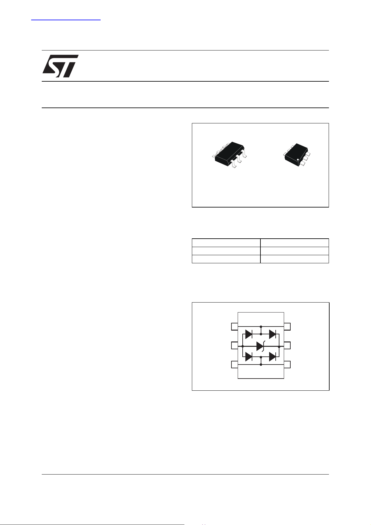
■ SOT-666 and SOT23-6L packages
■ RoHS compliant
BUS
USBLC6-2
VERY LOW CAPACITANCE
ESD PROTECTION
SOT23-6L
USBLC6-2SC6
Table 1: Order Codes
Part Number Marking
USBLC6-2SC6 UL26
USBLC6-2P6 F
Figure 1: Functional Diagram
SOT-666
USBLC6-2P6
BENEFITS
■ Very low capacitance between lines to GND for
optimized data integrity and speed
■ Ultra low PCB space consuming: 2.9mm² max
for SOT-666 package and 9mm² max for
SOT23-6L package
■ Enhanced ESD protection: IEC61000-4-2 level
4 compliance guaranteed at device level,
hence greater immunity at system level
■ ESD protection of V
. Allows ESD current
BUS
flowing to Ground when ESD event occurs on
data line
■ High reliability offered by monolithic integration
■ Very low leakage current for longer operation
of battery powered devices
■ Fast response time
■ Consistant D+/D- signal balance
- Best capacitance matching tolerance I/O to
GND of 0.04pF
- Compliance with USB2.0 requirement (<1pF)
June 2005
11
I/O1 I/O1
2
GND V
3
I/O2 I/O2
6
5
BUS
4
COMPLIES WITH THE FOLLOWING STANDARDS:
■ IEC61000-4-2 level 4:
15kV (air discharge)
8kV (contact discharge)
REV. 2
1/11
USBLC6-2
Table 2: Absolute Ratings
Symbol Parameter Value Unit
At device level:
V
Peak pulse voltage
PP
IEC61000-4-2 air discharge
IEC61000-4-2 contact discharge
MIL STD883C-Method 3015-6
15
15
25
kV
T
T
T
Table 3: Electrical Characteristics (T
Storage temperature range -55 to +150 °C
stg
Maximum junction temperature 125 °C
j
Lead solder temperature (10 seconds duration) 260 °C
L
= 25°C)
amb
Symbol Parameter Test Conditions
V
RM
I
RM
V
BR
V
V
CL
Reverse stand-off voltage 5 V
V
Leakage current
Breakdown voltage between V
and GND
Forward voltage
F
BUS
= 5V
RM
= 1mA
I
F
I
= 10mA
F
= 1A, tp = 8/20µs
I
PP
Any I/O pin to GND
Clamping voltage
I
= 5A, tp = 8/20µs
PP
Any I/O pin to GND
C
i/o-GND
∆C
Capacitance between I/O and GND
i/o-GND
V = 0V F = 1MHz
any I/O pin to GND
V = 0V F = 1MHz
C
i/o-i/o
Capacitance between I/O
between I/O, GND
not connected
Value
Unit
Min. Typ. Max.
1µA
6V
1.1 V
12 V
17 V
2.5 3.5
pF
0.04
1.2 1.7
pF
2/11
∆C
i/o-i/o
0.04
USBLC6-2
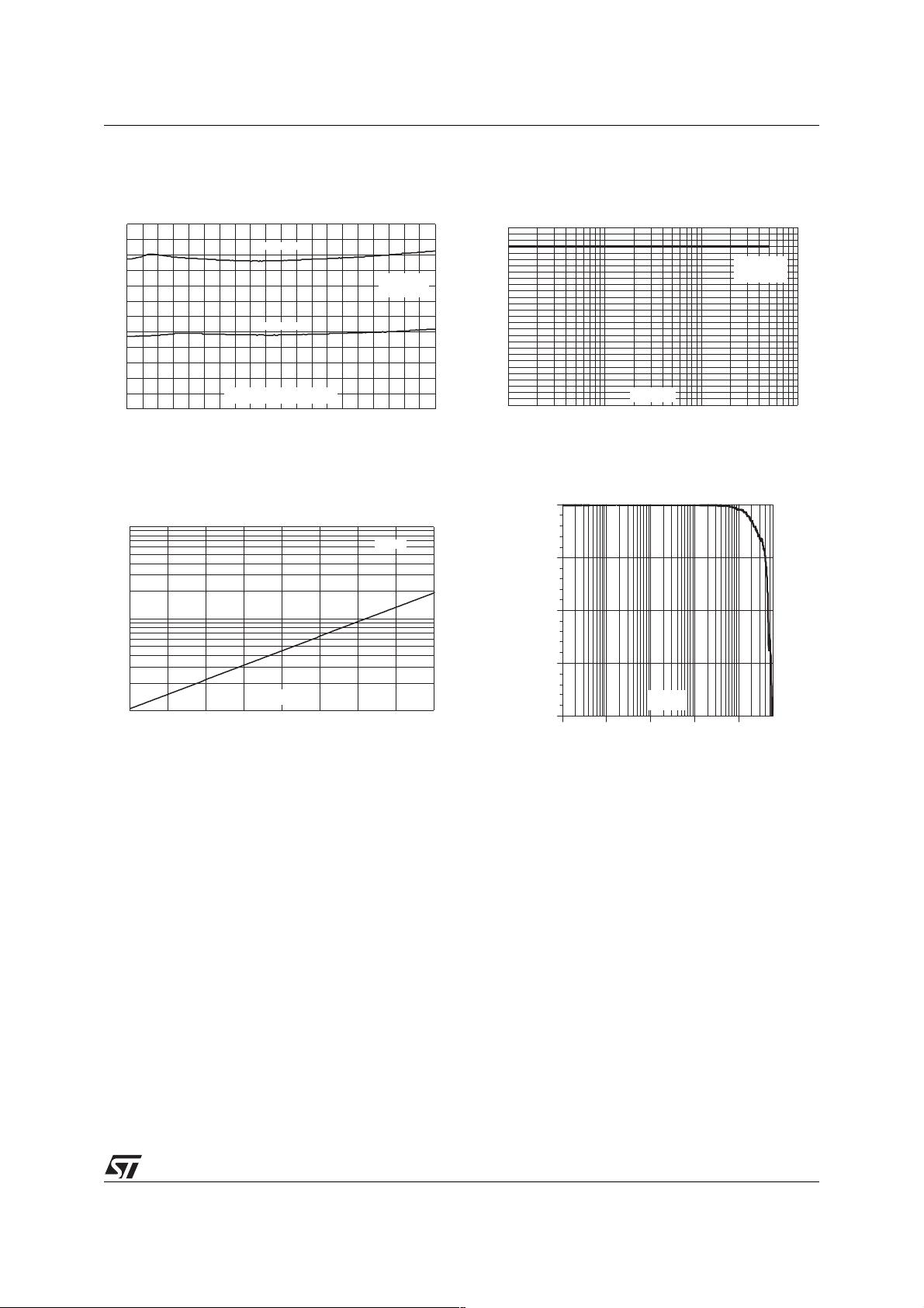
Figure 2: Capacitance versus line voltage
(typical values)
C(pF)
3.0
C =I/O-GND
2.5
2.0
1.5
1.0
0.5
O
C =I/O-I/O
j
F=1MHz
V =30mV
OSC RMS
T =25°C
j
Data line voltage (V)
0.0
0.0 0.5 1.0 1.5 2.0 2.5 3.0 3.5 4.0 4.5 5.0
Figure 4: Relative variation of leakage current
versus junction temperature (typical values)
I[T
] / I [T
100
RM j
10
RM j
=25°C]
V =5V
BUS
Figure 3: Line capacitance versus frequency
(typical values)
C(pF)
2.8
2.6
2.4
2.2
2.0
1.8
1.6
1.4
1.2
1.0
0.8
0.6
0.4
0.2
0.0
1 10 100 1000
F(MHz)
V =30mV
OSC RMS
T=25°C
j
V =0V to 3.3V
LINE
Figure 5: Frequency response
0.00
S21(dB)
-5.00
-10.00
T (°C)
1
25 50 75 100 125
j
-15.00
F(Hz)
-20.00
100.0k 1.0M 10.0M 100.0M 1.0G
3/11
USBLC6-2
TECHNICAL INFORMATION
1. SURGE PROTECTION
The USBLC6-2 is particularly optimized to perform surge protection based on the rail to rail topology.
The clamping voltage V
with: V
= VT + Rd.I
F
(VF forward drop voltage) / (VT threshold voltage)
We assume that the value of the dynamic resistance of the clamping diode is typically:
= 0.5Ω and VT = 1.2V.
R
d
For an IEC61000-4-2 surge Level 4 (Contact Discharge: V
approximation, we assume that : I
So, we find:
V
CL
V
CL
Note: the calculations do not take into account phenomena due to parasitic inductances.
2. SURGE PROTECTION APPLICATION EXAMPLE
If we consider that the connections from the pin V
two tracks of 10mm long and 0.5mm large; we assume that the parasitic inductances Lw of these tracks
are about 6nH. So when an IEC61000-4-2 surge occurs, due to the rise time of this spike (tr=1ns), the
voltage V
has an extra value equal to Lw.dI/dt.
CL
The dI/dt is calculated as: dI/dt = Ip/tr = 24 A/ns
The overvoltage due to the parasitic inductances is: Lw.dI/dt = 6 x 24 = 144V
By taking into account the effect of these parasitic inductances due to unsuitable layout, the clamping
voltage will be :
V
CL
V
CL
We can reduce as much as possible these phenomena with simple layout optimization.
It’s the reason why some recommendations have to be followed (see paragraph “How to ensure a good
ESD protection”).
can be calculated as follow :
CL
+ = V
V
CL
V
- = - VF for negative surge
CL
p
+ VF for positive surge
BUS
= Vg / Rg = 24A.
p
+ = +17V
- = -12V
+ = +17 + 144 = 161V
- = -12 - 144 = -156V
=8kV, Rg=330Ω), V
g
to VCC and from GND to PCB GND are done by
BUS
= +5V, and if in first
BUS
Figure 6: ESD behavior; parasitic phenomena due to unsuitable layout
183V
di
Lw
dt
VV
+
CC F
-V
di
-Lw
dt
-178V
4/11
ESD
SURGE
VI/O
Lw
Lw
F
V+ =
CL
V- =
CL
Lw
di
dt
V +V +Lw
BUS F
di
-V -Lw
F
dt
+V
CC
di
surge >0
dt
surge <0
V
BUS
V
I/O
di
dt
GND
F
V
tr=1ns
tr=1ns
CL
V
+
POSITIVE
SURGE
NEGATIVE
SURGE
-
CL
t
t
 Loading...